


1. Introduction
Amplifier is an important part of analog integrated circuits, so it is very important to design a high-performance amplifier for analog integrated circuits. Among the many parameters that affect amplifiers, researchers will especially focus on voltage gain in this paper and how to design an amplifier with high voltage gain. Voltage gain is the most basic parameter for operational amplifiers, which seriously affects the application of operational amplifiers. At the same time, with the continuous development of the integrated circuit manufacturing process, the size of MOSFET has been reduced to a few nanometers, and the voltage gain of a single MOSFET is limited, which poses a higher challenge for the design of high-gain integrated circuits. Therefore, it is crucial to use a series of gain improvement means to compensate for the gain degradation of mos tubes in integrated circuit design. This paper mainly focuses on the analysis and comparison of a series of existing gain enhancement technologies, and gives the advantages and disadvantages of each gain enhancement technology, hoping to provide a reference for the selection of gain enhancement technology in integrated circuit design.
2. Analysis and discussion of gain enhancement techniques
2.1. Cascode
Cascode amplifier is a common way to increase the voltage gain of amplifiers. The basic principle is to increase the output impedance of the circuit to increase the voltage gain of the circuit.
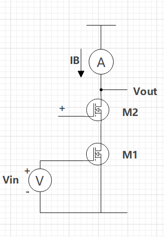
Figure 1. An ideal cascode amplifier.
Figure 1 shows an ideal cascode amplifier. In this circuit, an ideal current source LB is used to bias the circuit, and M2 MOSFET acts as a similar current buffer, increasing the output impedance of the circuit and thus increasing the total voltage gain of the circuit. Under ideal conditions, the total voltage gain can reach the product of the voltage gain of two MOSFETs.
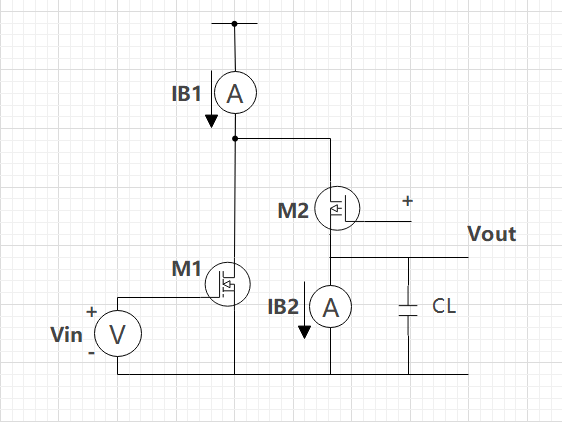
Figure 2. An ideal folded cascode amplifier.
Figure 2 shows a typical folded cascode amplifier. The principle of high voltage gain reached by this structure is the same as that of cascode structure, and most of the parameters except current loss are also roughly the same, but because of its advantages in use as a differential circuit, it is worthy to be discussed separately here.
Both of these amplifiers have upsides and downsides. Start with the ideal cascode amplifier, the most prominent feature of ideal cascode amplifier is that it can reach a high voltage gain with a ideal current source as bias or under low frequency high load conditions. Based on the above statement of the advantages of cascade structure, the disadvantages of the cascode amplifier are also very clearly. Without DC current source bias or low-frequency high load conditions, its ability to increase voltage gain is greatly reduced. At the same time, it is also necessary to consider that the ideal current source does not exist in the real world. Therefore, it is necessary to simulate an ideal current source as much as possible. As a result, a telescopic cascode amplifier is produced, which used two MOSFETs in series as a current source. But it will seriously lead to a drop in the output voltage swing. In a telescopic cascode amplifier the Possible maximum output voltage swing is equal to the power supply voltage minus the sum of the four mos overdrive voltages, in most cases this sum is 0.8V, which means, if a relatively small voltage is used in the circuit, such as 1 or 2 V, this weakness will badly influence the output voltage swing.
Then move on to the folded cascode amplifier. folded cascode amplifier is similar to the Cascode amplifier and has similar advantages and disadvantages. But what the difference is that the folded cascode amplifier is really meaningful when used as a differential circuit. The input and output of the folded cascode amplifier can be shorted, the selection of the input common-mode level is easier, and the output voltage swing is larger than that of the ordinary cascode amplifier. However, it also has a disadvantage that cannot be ignored, because the bias current will be evenly distributed between the two transistors, which will lead to the current consumption of the folded cascode amplifier will be twice that of the cascode amplifier under the same voltage gain, output swing and gain bandwidth product, these are really the shortcoming of the folded cascode amplifier.
At present, the above two technologies have been widely used in the field of integrated circuit design, and they are common means to improve amplifier gain. Here, I hope to discuss the future development prospects of this technology based on previous research. Due to the wide application of the folded cascode amplifier in differential circuits, the folded cascode amplifier is significantly more used than the ordinary cascode amplifier. At the same time, the current integrated circuit design is developing in the direction of high speed, low voltage and low power [1]. Talwar, Sharma and Srivastava discussed and compared the folded cascode amplifier of the circulating type and the complementary type, which have the advantages of saving power, sedimentation time, circuit area and increasing bandwidth, which are of great significance in mobile communication [2]. At the same time, as a single-pole amplifier circuit, the folded cascode amplifier has a high speed, which makes it very suitable for use in the field of mobile communication, but in another side, the problem of poor anti-noise ability of the folded cascode amplifier itself must be fully considered, which will be one of the future research directions.
2.2. Cascade
The cascade amplifier is also a very common amplifier, which used to increase the voltage gain of the amplifier, and its basic principle is to achieve the increase of the total voltage gain by connecting multiple single-pole amplifier circuits.
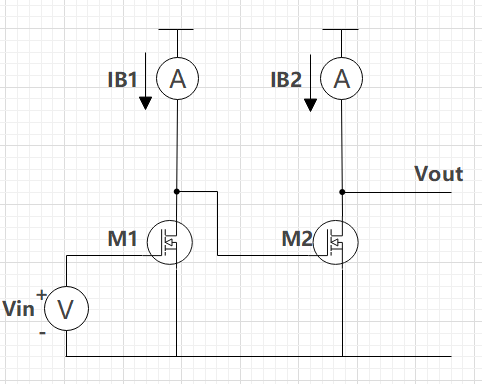
Figure 3. A typical cascade amplifier.
Figure 3 shows a typical cascade amplifier with two single-staged amplifiers connected, and the total voltage gain can also be obtained as the product of all single-staged amplifiers' voltage gains under ideal conditions.
The most compelling advantage of cascade amplifiers is their ability to increase voltage gain, by connecting multiple single-staged amplifiers a higher voltage gain and higher output swing can be easily obtained [3]. Meanwhile, cascade amplifiers have great advantages in reducing the output signal-to-noise ratio compared with single staged amplifiers. Using a circuit with a low noise factor in the first stage of cascade amplifiers can improve the noise factor of the entire circuit [4]. Its disadvantages are also obvious, the speed of the cascade amplifier is much lower than that of the single-stage amplifier, which makes it very unfavorable in the field of high-speed demand such as communication. The high-power consumption of the cascade amplifier circuit is also one of its disadvantages, and this problem needs to be considered by designers under the current design concept of pursuing low power consumption. In addition, there is also the problem of stability in the cascade structure, in order to solve this problem, it is often necessary to add a Miller capacitor between the two stages of the amplification circuit to compensate, and this will also lead to additional circuit power consumption increase.
The amplifier of the cascade mechanism is also widely used at present. In the design, it is often considered to use a multistage amplifier circuit to achieve a high-gain and high-swing circuit through the cascade of the high-gain stage and the high-swing stage [3], and at the same time, it can also obtain a better bandwidth. However, the current development trend of integrated circuits tends to be high energy efficiency and high integration. For this reason, the larger area and higher power consumption of multistage amplifier circuits will be a problem that needs to be further solved. These could be the most important future research directions in this field.
2.3. Gain boosting
As with the above two techniques, the gain boosting is a kind of technique that increases the voltage gain of the circuit by increasing the output impedance of the circuit.In deep submicron CMOS technology, even if the cascode amplifier is used, a relatively ideal voltage gain cannot be reached, so feedback technology can be considered to improve the voltage gain.\
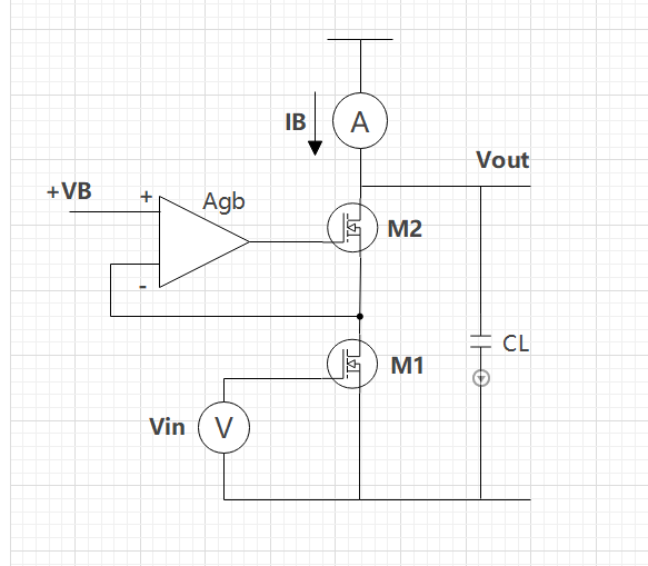
Figure 4. A typical case using gain boosting.
Figure 4 is a typical single-staged amplifier circuit using the gain boosting technique.A large gain operational amplifier is used as feedback in the circuit. According to the virtual short circuit and virtual open circuit characteristic of the operational amplifier, the source voltage of the transistor M2 is constant, thus making the current fixed, which makes the feedback structure form a better current source. It also can be seen from the small-signal circuit analysis. Under ideal conditions, the output impedance of the circuit is Agb times higher than that of the original cascode amplifier. The voltage gain is also Agb times higher than original voltage gain. The voltage gain of the circuit can be seen to be improved by several orders of magnitude.
Similar to other methods of increasing voltage gain, gain-boosting technology can improve voltage gain well, and its voltage gain is higher than that of common single-pole amplifiers such as cascode amplifiers. However, the high gain of gain-boosting technology comes at the cost of speed, which limits its use in the fields of communications, medicine, and automation. In addition, the gain enhancement technology will also lead to high power consumption of the circuit, which is not good to some low-power design [5]. At the same time, gain enhancement technology will also bring some stability problems. The circuit itself has a zero-pole pair, and to compensate for it, the unit gain bandwidth of the auxiliary op amp needs to be increased. When the unit gain bandwidth frequency of the auxiliary op amp increases near the second node of the circuit, the entire op-amp will be unstable [6].
The gain-boosting technique is especially widely used in multistage amplifiers because of its excellent gain-boosting ability to obtain higher voltage gains than ordinary cascode amplifier, which makes it often used as a gain-boosting stage of multistage amplifier circuits [6, 7].In addition, Hui, Woo,Hung and Leung proposed an amplifier with double gain boosting technology, which has a good increase in both gain boosting and output voltage swing [8]. Meanwhile, Chang and Lin also proposed a structure named double self-bias topology, in which a single power supply can be used for power supply and gain enhancement can be improved to achieve low power consumption and high gain [9].
2.4. Bootstrapping
Bootstrapping is a technology that achieves high voltage gain by bootstrapping the effective value of output resistance. Similar to the gain boosting technology which mentioned earlier, it has great significance in deep submicron CMOS technology.
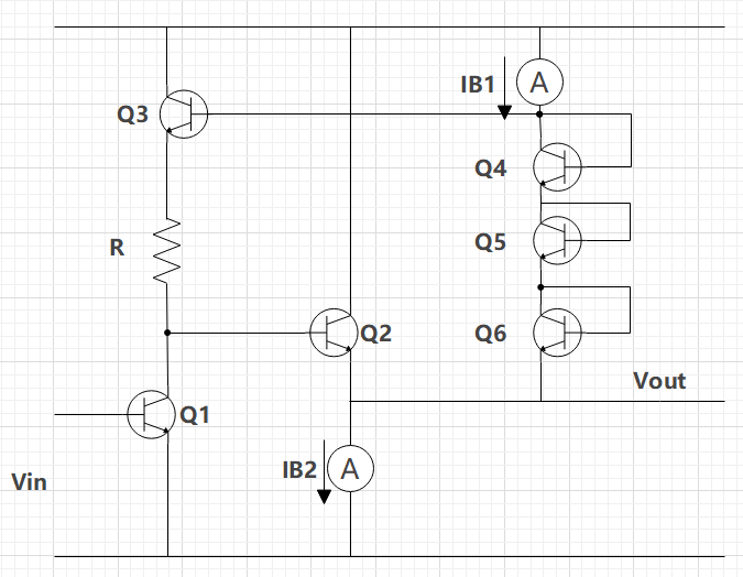
Figure 5. A case using bootstrapping to improve voltage gain.
Figure 5 is an example of a circuit that uses bootstrap technology.In this circuit, Q1 is the amplifier.Q2 is the emitter follower. The load resistance is connected to another emitter follower Q3. Q3 is connected to the output voltage through three diodes. The output AC voltage of the emitter follower Q3 is the same as the collector AC voltage of the input transistor Q1. For this reason, there is no AC voltage drop at both ends of the resistance R. So the resistance R is bootstrapped to a large value.
One of the great implications of bootstrap technology is its ability to increase voltage gain. In the integrated circuit design can be combined with another high-gain circuit mechanism to get a more ideal effect, but also can get a larger bandwidth also has a good performance. However, the same bootstrap technique results in slower circuit speeds and higher power consumption compared to the cascode amplifier. At the same time, because the technology requires adding circuits to the original circuit, this can lead to possible stability problems.
In addition to the great performance of bootstrap technology in increasing voltage gain, it also has a good performance in improving linearity. In the paper [10, 11], the author used bootstrap technology in the design of amplifier circuits to improve the output impedance, so as to improve the linearity of the circuit [12].In addition, in the paper [11], a neutral bootstrap common-source common-gate amplifier topology is proposed, which can maintain stability while improving power gain and output voltage swing [11].It can be concluded from the above that the current application of bootstrap technology is not limited to improving voltage gain, but also has a good effect on improving other parameters of the circuit. This is also different from the gain enhancement technology, its application is more flexible.
3. Conclusion
In this paper, four methods to improve voltage gain are discussed in detail. In today's MOSFET size is further reduced, its voltage gain ability is also affected to a certain extent, so it is essential to compensate it by means of increasing voltage gain. The cascode Amplifier is a basic and effective gain-enhancing amplifier, and its greatest significance is that the remaining three technologies can often be constructed on the basis of the thecascode AmplifierThe cascade structure can achieve different parameter requirements by connecting different single-stage amplifiers, which is a very flexible structure, but there will be problems such as stability and speed. The gain boosting technology can further improve the voltage gain on the basis of the cascode amplifier, so it has great significance in improving the gain.Finally, there is bootstrap technology, which not only increases the gain, but also has applications in improving linearity. The above is a simple summary of the four technologies, but it is worth noting that the analysis of these technologies in this paper is stuck in the theoretical aspect and lacks practical verification, which needs to be further improved.
References
[1]. Kammari R Gundla J Boyapati S Pasupureddi V S R 2022 Modeling and Design of A Compact Low Power Folded Cascode OpAmp With High EMI Immunity IEEE Trans Electromagn Compat vol 64 no 2 pp 595-598
[2]. Talwar V Sharma T Srivastava S 2021 A Survey on Comparison of Complementary and Recycling Folded Cascode Amplifier for Different Parameters 2021 9th Int Conf Reliab Infocom Technol Optim (ICRITO) Noida India pp 1-3
[3]. Bambo Jiang Yanfeng 2015 A High Gain Multistage Operational Amplifier Design J Microelectron (6) pp 706-709
[4]. Song Qing Wang Qiang Yang Zongshuai 2014 Derivation of Noise Factor Formula of Cascade Amplifier and a Novel Understanding Method Exp Sci Technol vol 12 no 06 pp 33-35
[5]. Ramaraj K 2023 Improvement of the Effective Bandwidth of Multistage Amplifier by Cascading the Individual Two Stage Feedback Amplifiers 2023 Int Conf Self Sustain Artif Intell Syst (ICSSAS) Erode India pp 1714-1718
[6]. Song Qiwei Lu Anjiang Zhang Zhengping 2012 With a Gain to Improve the Technology of High-Speed CMOS Operational Amplifier Design J Electron Des Eng vol 20 no 10 pp 1-4
[7]. Wang Xuequan Liang Qi 2006 Design of a High-Gain CMOS Operational Amplifier with Gain Enhancement Mod Electron Technol no 12 pp 148-150
[8]. Hui H W Woo Y H Hung C H Leung K N 2018 A Double Gain-Boosted Amplifier with Widened Output Swing Based on Signal-and Transient-Current Boosting Technique in CMOS 130-nm Technology 2018 IEEE Int Conf Electron Devices Solid State Circuits (EDSSC) Shenzhen China pp 1-2
[9]. Chang J F Lin Y S 2024 3.8-mW 26–29-GHz CMOS LNA With 21.6-dB Gain and 2.49-dB NFavg Using Dual Self-Bias and Gain Boosting IEEE Microw Wirel Technol Lett vol 34 no 1 pp 72-75
[10]. Kumar R R Sharma K 2023 Design and Simulation of Enhanced Bootstrapping Technique Based Low Power Operational Transconductance Amplifier 2023 Int Conf Artif Intell Smart Commun (AISC) Greater Noida India pp 48-51
[11]. Zhao D Reynaert P 2015 A 40-nm CMOS E-Band 4-Way Power Amplifier With Neutralized Bootstrapped Cascode Amplifier and Optimum Passive Circuits IEEE Trans Microw Theory Techn vol 63 no 12 pp 4083-4089
[12]. Cinco-Izquierdo O J de la Cruz-Blas C A Sanz-Pascual M T 2022 High-Linearity Tunable Low-Gₘ Transconductor Based on Bootstrapping IEEE Trans Circuits Syst II Express Briefs vol 69 no 2 pp 259-263
Cite this article
Chen,D. (2024). Analysis of Gain Enhancement Techniques in Integrated Circuit Design. Applied and Computational Engineering,103,17-23.
Data availability
The datasets used and/or analyzed during the current study will be available from the authors upon reasonable request.
Disclaimer/Publisher's Note
The statements, opinions and data contained in all publications are solely those of the individual author(s) and contributor(s) and not of EWA Publishing and/or the editor(s). EWA Publishing and/or the editor(s) disclaim responsibility for any injury to people or property resulting from any ideas, methods, instructions or products referred to in the content.
About volume
Volume title: Proceedings of the 2nd International Conference on Machine Learning and Automation
© 2024 by the author(s). Licensee EWA Publishing, Oxford, UK. This article is an open access article distributed under the terms and
conditions of the Creative Commons Attribution (CC BY) license. Authors who
publish this series agree to the following terms:
1. Authors retain copyright and grant the series right of first publication with the work simultaneously licensed under a Creative Commons
Attribution License that allows others to share the work with an acknowledgment of the work's authorship and initial publication in this
series.
2. Authors are able to enter into separate, additional contractual arrangements for the non-exclusive distribution of the series's published
version of the work (e.g., post it to an institutional repository or publish it in a book), with an acknowledgment of its initial
publication in this series.
3. Authors are permitted and encouraged to post their work online (e.g., in institutional repositories or on their website) prior to and
during the submission process, as it can lead to productive exchanges, as well as earlier and greater citation of published work (See
Open access policy for details).
References
[1]. Kammari R Gundla J Boyapati S Pasupureddi V S R 2022 Modeling and Design of A Compact Low Power Folded Cascode OpAmp With High EMI Immunity IEEE Trans Electromagn Compat vol 64 no 2 pp 595-598
[2]. Talwar V Sharma T Srivastava S 2021 A Survey on Comparison of Complementary and Recycling Folded Cascode Amplifier for Different Parameters 2021 9th Int Conf Reliab Infocom Technol Optim (ICRITO) Noida India pp 1-3
[3]. Bambo Jiang Yanfeng 2015 A High Gain Multistage Operational Amplifier Design J Microelectron (6) pp 706-709
[4]. Song Qing Wang Qiang Yang Zongshuai 2014 Derivation of Noise Factor Formula of Cascade Amplifier and a Novel Understanding Method Exp Sci Technol vol 12 no 06 pp 33-35
[5]. Ramaraj K 2023 Improvement of the Effective Bandwidth of Multistage Amplifier by Cascading the Individual Two Stage Feedback Amplifiers 2023 Int Conf Self Sustain Artif Intell Syst (ICSSAS) Erode India pp 1714-1718
[6]. Song Qiwei Lu Anjiang Zhang Zhengping 2012 With a Gain to Improve the Technology of High-Speed CMOS Operational Amplifier Design J Electron Des Eng vol 20 no 10 pp 1-4
[7]. Wang Xuequan Liang Qi 2006 Design of a High-Gain CMOS Operational Amplifier with Gain Enhancement Mod Electron Technol no 12 pp 148-150
[8]. Hui H W Woo Y H Hung C H Leung K N 2018 A Double Gain-Boosted Amplifier with Widened Output Swing Based on Signal-and Transient-Current Boosting Technique in CMOS 130-nm Technology 2018 IEEE Int Conf Electron Devices Solid State Circuits (EDSSC) Shenzhen China pp 1-2
[9]. Chang J F Lin Y S 2024 3.8-mW 26–29-GHz CMOS LNA With 21.6-dB Gain and 2.49-dB NFavg Using Dual Self-Bias and Gain Boosting IEEE Microw Wirel Technol Lett vol 34 no 1 pp 72-75
[10]. Kumar R R Sharma K 2023 Design and Simulation of Enhanced Bootstrapping Technique Based Low Power Operational Transconductance Amplifier 2023 Int Conf Artif Intell Smart Commun (AISC) Greater Noida India pp 48-51
[11]. Zhao D Reynaert P 2015 A 40-nm CMOS E-Band 4-Way Power Amplifier With Neutralized Bootstrapped Cascode Amplifier and Optimum Passive Circuits IEEE Trans Microw Theory Techn vol 63 no 12 pp 4083-4089
[12]. Cinco-Izquierdo O J de la Cruz-Blas C A Sanz-Pascual M T 2022 High-Linearity Tunable Low-Gₘ Transconductor Based on Bootstrapping IEEE Trans Circuits Syst II Express Briefs vol 69 no 2 pp 259-263