


1. Introduction
Low Dropout Regulator (LDO) has rapidly become one of the most widely used types of power management chips because of its simple structure, fast response, small output ripple and other outstanding advantages. The small size and easy integration of LDOs make them increasingly utilized in today's environment of chip integration, and they have been heavily integrated into a wide range of chips for use as modules. However, the contradiction between the response rate requirements of highly integrated circuits and the outputs of the chip's complex circuits is becoming more and more prominent, that is the reason why LDO module requires fast transient response capabilities [1]. According to above questions, four methods are proposed in this study, introducing the influencing factors and improvement principles of each method one by one, and comprehensively comparing their advantages and disadvantages with the applicable situation.
2. LDO Chip Overview
LDO is a type of voltage regulator, its basic function is to output a stable voltage within a certain range of input voltage variation and load variation.
As an important part of the power management unit, the LDO has the characteristics of simple structure, rapid response and small output ripple, widely used in various types of chips. The biggest difference between an LDO chip and a three-terminal regulator is that it is a miniature system-on-chip (SOC) with very low self-consumption.
LDO chips can be used for current master channel control. It integrates hardware circuits such as MOSFET with very low on-line on-resistance, Schottky diodes, sampling resistors and voltage divider resistors on top. Functions include over-current protection, over-temperature protection, a precision reference source and a differential amplifier.
LDO chip in low-power module design, a novel structure of bandgap reference source, undervoltage latch circuit and low-power oscillator is proposed, cleverly utilizes the threshold characteristics of MOS tubes for design, which saves resistor layout area, reduces quiescent current consumption, and has a certain temperature compensation effect. Second, a smooth transition buffer stage is introduced in the main loop to reduce the quiescent on-state current and power consumption while guaranteeing the performance of the main loop.
In terms of transient response, a novel loop compensation method under low power consumption is proposed. It improves the loop stability as well as the transient response performance. Meanwhile, a transient boosting self-biased current source and a fast response loop are proposed, which can maintain low quiescent current consumption during output stabilization and improve the transient response performance of the loop during load transient changes.
3. LDO Chip Operation Analysis
The circuit diagram of the LDO chip is shown in Figure 1, which mainly consists of a voltage reference circuit, an error amplifier, a feedback resistor, and a transistor adjustment circuit. The whole circuit can be regarded as a voltage follower that can output large current with high load carrying capability.
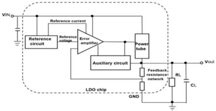
Figure 1. Internal structure of LDO chip [2].
The voltage reference circuit provides a reference voltage (Vref) for the entire LDO circuit that is independent of process conditions, supply voltage, and temperature.
The error amplifier is responsible for connecting the FET and the feedback resistor, which complement each other to form a negative feedback circuit to realize the voltage stabilization function of the LDO chip.
The transistor adjustment circuit is responsible for outputting this amplified signal to the control pole of the transistor (that is, the gate of the PMOS tube), so that this amplified signal (current) can control the on-state voltage of the transistor, which is a negative feedback adjustment loop. With the increasing integration of circuits, LDO chips without off-chip capacitance have gradually become a development trend, it will face challenges in system stability and load transient response performance. When the load of the LDO is a clocked digital circuit such as an MCU, FPGA, etc., the LDO can be used for a variety of purposes. Dramatic changes in load current result in the LDO not being able to instantly adjust the overshoot voltage due to the output current. causing an impact on the proper functioning of the circuit. Therefore, it is very significant to investigate how to improve the load transient response performance of LDOs without off-chip capacitance.
4. Principles of Operation
The basic structure of a linear regulator is shown Figure 2 and consists of an error amplifier, a power tube, a feedback network, a bandgap reference circuit, and an auxiliary circuit [3].
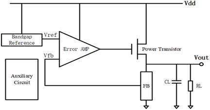
Figure 2. LDO circuit structure [3].
LDO circuits work mainly to stabilize the output voltage when the load change causes a change in the supply voltage as well as its output current. The feedback network consists of two feedback resistors (R1, R2) fed back to the \( V_{fb} \) port of the error amplifier by capturing the output voltage, while the \( V_{ref} \) port of the error amplifier is a reference voltage unaffected by variations in process, supply voltage, and temperature provided by a bandgap reference circuit. Then the error amplifier amplifies the difference between the them and outputs it to the gate of the power transistor. The power transistor adjusts its output current according to the change in gate voltage, which affects the change in final output voltage. The expression for the LDO static operating point is as follows( \( A_{error\ amp} \) is the gain of the error amplifier, \( A_{power\ MOS} \) is the gain of the power tube):
\( V_{out}=V_{ref}\frac{A_{error\ amp}\bullet A_{power\ MOS}}{\left(\frac{R_1}{R_2}+1\right)A_{error\ amp}\bullet A_{power\ MOS}+1} \) (1)
For example, when the output voltage becomes small, the voltage fed back from the feedback network to the error amplifier also becomes small, so that the voltage output from the error amplifier to the gate of the power transistor becomes small and the absolute value of the voltage difference between the source of the power transistor and the gate of the power transistor becomes large, and then the output current of the power transistor becomes large to increase the output voltage to form a negative feedback effect. The current equation of the power transistor is as follows with the transfer characteristic curve of the PMOS tube in Figure 3.
\( I_{Dpmos}=\frac{1}{2}\mu_PC_{ox}\frac{W}{L}\left(V_{GS}−V_{THp}\right)^2 \) (2)
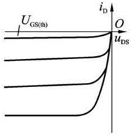
Figure 3. PMOS transfer characteristic.
5. Transient Response LDO Characterization Theory
Ideally, the output voltage should be stable regardless of changes in the supply voltage or load of the LDO. However, the regulation characteristics of the circuit result in a certain time difference between the output voltage and the change in the regulator after a load change. This unavoidable delay results in a short sharp change in the output voltage, which is the transient response. Figure 4 shows the transient response curve of the load current of the LDO from light load to heavy load and then from heavy load to light load.
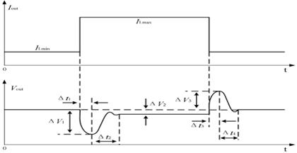
Figure 4. LDO transient response curve [4].
For example, when the LDO load current \( I_{OUT} \) from light load \( I_{Lmin} \) to heavy load \( I_{Lmax} \) , the output current suddenly increases because the power tube cannot respond in time. Load capacitance amplification leads to the LDO output voltage \( V_{OUT} \) will be instantly reduced, and then after the circuit control loop feedback control power tube changes, the output voltage will be back up and back up too quickly there will be fluctuations. Similarly, when the load current changes from a heavy load to a light load, the output voltage \( V_{OUT} \) rises momentarily and then decreases and stabilizes. \( ∆V_{1} \) denotes the undershoot voltage magnitude, \( ∆V_{2} \) denotes the overshoot voltage magnitude, \( ∆t_{1} \) denotes the undershoot time, \( ∆t_{3} \) denotes the overshoot time, \( ∆t_{2} \) denotes the undershoot recovery time, and \( ∆t_{4} \) denotes the overshoot recovery time. These are important parameters in the transient response process.
6. Transient Response LDO Optimization Strategy Analysis
Conventional LDO chips often require an off-chip capacitor at the output to store charge, in turn maintains loop stability and system transient response.But large capacitors not only increase the chip area, but also cause defects in the output voltage waveform. Therefore, the LDO chip without off-chip capacitance becomes an important research trend.
The analysis also concludes that the transient response performance can be improved by increasing the bandwidth or increasing the drive current.
Figure 5 shows an equivalent circuit diagram of the output side of the LDO, where indicates the load capacitance of the LDO ,indicates the bypass capacitance of the LDO, and indicates the equivalent series resistance of the LDO load.
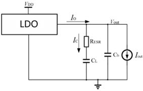
Figure 5. LDO Output equivalent diagram [3].
The overshoot and undershoot voltages are calculated as follows:
\( \ ∆V_{TR}= \frac{∆I_{out}}{C_{L}+C_{b}}∙∆t+\frac{C_{L}}{C_{L}+C_{b}}∆I_{out}R_{ESR} \) (3)
In the above equation, the indicates the amount of change in load current at output, is the undershoot time or overshoot time of the LDO. It can be found from this that the magnitude of the LDO overshoot and undershoot voltages are related to the load capacitance, the bypass capacitance, the equivalent series resistance of the load, and the amount of variation in the output current, as well as the undershoot duration or overshoot duration.
6.1. Reducing the equivalent series resistance in the load capacitance
The external capacitance is to compensate for the LDO loop to stabilize the circuit, and for LDO circuits without off-chip capacitance, the load capacitance at the output is very small and does not introduce an equivalent series resistance. And since circuits without off-chip capacitance make the circuit less stable, it requires a large compensation capacitance, however, when a large capacitance is introduced at the gate of the power tube, the step output current load results in a long response time and a large overshoot or overshoot due to the large total capacitance of charging or discharging [5]. The Figure 6 shows a new capacitor multiplier compensation scheme, which is equivalent to a small capacitor in the case of small or large signals, with the advantages of improved transient response and high stability.
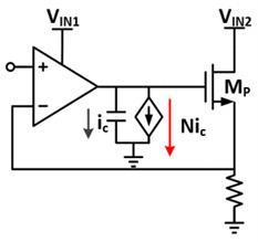
Figure 6. Capacitor-Less LDO circuit [6].
The principle according to the current mode multiplier in Figure 7(a) below is to amplify the capacitive effect through current scaling [7]. The current through \( M_{c2} \) is approximated as \( i_c=sVC_c \) , the total current of capacitance multiplier in Figure 7(b) is (N+1) \( i_c \) , and the equivalent capacitance value is the current led by \( C_c\left(N+1\right) \) . It can be found that \( {gmc}_1 \) and \( {gmc}_2 \) are the transconductance of \( {Mc}_1 \) and \( M_{c2} \) will affect the low frequency circuit and its capacitive bandwidth is affected by the impedance 1/ \( g_{mc2} \) , so it is necessary to minimize the transconductance of \( {gmc}_2 \) so that the capacitance does not become a large capacitance, which results in the impact of transient response. The following equation shows the equivalent capacitance \( C_{eq}(s) \) of the capacitance multiplier:
\( C_{eq}\left(s\right)=C_c(1+N)\frac{1}{1+sC_c/g_{mc2}} \) (4)
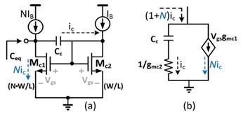
Figure 7. Equivalent circuit of the input impedance of Capacitance multiplier [6].
6.2. Use of capacitively coupled current mirrors
The traditional LDO circuit structure is slightly modified by adding a voltage buffer stage circuit between the error amplifier and the power tube, as shown in Figure 8, this results in a more stable loop by pushing the non-primary poles in the power transistor to high frequencies. At the same time, the increased output impedance shifts the main poles to lower frequencies, contributing to loop stabilization. Thus, the addition of transient response circuitry improves the overall response rate of the chip, the disadvantage is that the capacitively coupled current mirrors take some time to reach steady state, which results in slower startup.
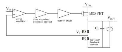
Figure 8. LDO circuit schematic diagram [8].
The design utilizes a transient response circuit with capacitively coupled current mirrors, Increase the gate drive current of the power tube. The enhancement circuit consists of M22~M30 field effect tubes, resistors R5 and R6, capacitors C1 and C2. The principles of operation under heavy and light loads are shown respectively in Figure 9 and Figure 10. When \( V_{OUT} \) is in steady state, since the capacitor voltage cannot transiently, the gate voltage of M24 and M26 is determined by VB4 and the output current is constant.
When the output jumps heavy load, as the voltage divider effect of R5 and R6 and the high pass characteristics of C1 and C2, the upstroke voltage coupled to the gate voltage of M24 and M26, and the gate voltage of the M26 tube increase. When the M24 tube cutoff, the M26 drain current increases, coupling the current mirrors M27 and M28. Then the gate discharge current of the power converter MP increases instantaneously.
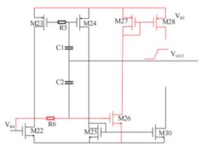
Figure 9. Schematic diagram for output tripping under heavy load [8].
When the output jumps light load, R5 and R6 divide the voltage, and C1 and C2 have a high-pass characteristic that makes the downstroke voltage will be coupled to the gate voltage of M24, M26, increasing the gate voltage of the M24 tube, cutting off the M26 tube, expanding the M24 drain current. This results in enhanced transient response.
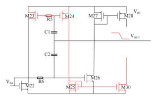
Figure 10. Schematic diagram for output tripping under light load [8].
6.3. Reducing overshoot and undershoot durations
It can be found from the formulas for overshoot and undershoot voltages that the overshoot or undershoot voltage can be reduced when the overshoot or undershoot duration is shortened. The undershoot duration (overshoot duration) can be derived from the following formula:
\( ∆t_{1}(∆t_{3})=\frac{1}{BW_{CL}}+C_{b}\frac{∆V_{b}}{I_{SR}} \) (5)
In the above equation, \( BW_{CL} \) denotes the loop bandwidth of the LDO, \( ∆V_{b} \) denotes the amount of voltage variation of the bypass capacitor, and \( I_{SR} \) denotes the drive current of the power tube. To further improve the performance of the LDO transient response, a fast response channel can be created from the LDO output to the gate of the power tube. In figure 11, \( V_{b1} \) and \( V_{b2} \) are the bias voltage, \( V_{out} \) is the LDO output voltage, switch K1 is the low level conduction switch PMOS tube, switch K2 is the high level conduction NMOS tube, and \( V_G \) is the power tube gate voltage.
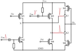
Figure 11. Transient Enhancement Circuit [4].
When the circuit works stably, switch K1 is disconnected, switch K2 is disconnected, and the entire transient response circuit does not work and consumes zero power when the LDO circuit works stably. And the output \( V_G \) is only controlled by the main control circuit of the feedback loop and is not affected by the transient response circuit.
When the output of the LDO transient response occurs, when \( V_{out} \) suddenly decreases, switch K2 opens, the power tube gate is discharged by M6, and the voltage \( V_G \) instantly decreases; when \( V_{out} \) suddenly increases, switch K1 opens, the power tube gate is charged by M5, and the voltage \( V_G \) instantly increases.
Since the overall feedback loop via the error amplifier takes much longer than the feedback time for transient enhancement, which may cause the transient enhancement circuit to cause a transition charging or discharging of \( V_G \) , it is limited using two diodes connected to M5 and M6.
The advantage of this method is that it can further improve the response speed of the LDO output changes to the gate end of the power tube to reduce the overshoot or undershoot time to improve the performance of the transient response, but also to avoid the transient response circuit itself brought about by over-discharging and over-charging defects. However, the disadvantage is that it will make the circuit become more complex and increase the cost.
6.4. Adoption of dual feedback loop structure
Conventional LDO typically utilizes a single feedback loop structure, that structure is more difficult to balance loop gain and bandwidth usage frequency compensation. And the dual feedback loop solves these problems.
For a single feedback loop with two stages of amplification, the transfer function is as followed:
\( H_s\left(s\right)=A_1A_2\beta\frac{1}{(1+\frac{f}{p_1})(1+\frac{f}{p_2})} \) (6)
Where A1, A2, β are the low-frequency gain and feedback network gain of the first and second stage amplifiers, p1, p2 are the pole frequencies of the output nodes of the first and second stage with a gain of A1A2β.
At this point the output is fed back to the input of the second stage amplifier, a double feedback loop can be formed and a new transfer function can be obtained:
\( H_d(s)=\frac{A_1A_2\beta_1}{(1+\frac{s}{p_1})(1+\frac{s}{p_2})}+\frac{A_1A_2}{(1+\frac{s}{p_2})} \) (7)
The gain is A1A2β+A2 and the bandwidth is GBWd.
From the above, it can be seen that the unit gain and closed loop bandwidth of the dual feedback loop are greater than that of the single loop[9]. And a dual feedback circuit can be proposed as in Figure 12.
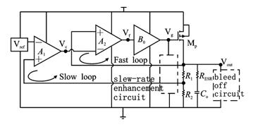
Figure 12. LDO Architecture with Dual Loop Feedback [10].
Wherein a fast loop is formed between the output and the input of the second-stage amplifier.
Three poles exist in the fast loop, adding two more zero points can be compensated for to get a larger bandwidth, enabling the circuit to have sufficient phase margin even under extreme conditions with zero load. Stability is improved and a fast transient response is possible.
With this method, good transient response can be achieved for large sudden changes in load current, meanwhile ensuring relatively low quiescent current, high closed-loop gain and system stability. The downside is that the loop becomes complex, the energy consumption increases, and the requirement for capacity charge relief capability can be increased [10].
7. Conclusion
This paper investigates several methods of realizing high transient response LDO. The advantages and disadvantages of different methods are evaluated by comparing research results and design concepts of different methods in the world. Finally, it was found that shortening the overshoot and undershoot durations by building transient enhancement circuits was the best among the above research methods in terms of performance. The principle is not only simple, it also greatly improves the response time and avoids the defects of over-discharge and over-charge. Reducing the equivalent series resistance of the load capacitance can be accomplished by using capacitor-less LDO circuit. Its load capacitance and equivalent series resistance are very small. However, its stability is harder to control. Adding compensation circuits improves stability but also makes the circuit more complex. The method of capacitively coupled current mirrors can push the non-primary poles to high frequencies and help the loop to be more stable. Its disadvantage is that capacitively coupled current mirrors take some time to reach steady state resulting in a longer startup time for the LDO. The dual-feedback loop structure increases the circuit's load current mutation to ensure low quiescent current, high closed-loop gain and high stability. However, its high complexity of circuits and high energy consumption makes circuits more costly. Further optimization in the above research methodology can be carried out in the future, e.g., using different compensation schemes to simultaneously improve the stability and transient response performance of the circuit, leading to an in-depth study of the topic.
Authors Contribution
All the authors contributed equally and their names were listed in alphabetical order.
References
[1]. Chen D P He L N and Yan X L 2006 An LDO linear regulator with low quiescent current and high stability Journal of Electronics and Information pp 1526–1529
[2]. Wu K 2024 Application Research Progress of LDO Chips Highlights in Science Engineering and Technology 103 pp 48–52
[3]. Song S Chen J Yuan H et al 2022 A low-noise and fast transient response LDO design for high-speed SerDes Journal of Physics Conference Series IOP Publishing 2187(1) 012006
[4]. Liu Z F 2023 Research and design of fast transient response LDO without off-chip capacitance Jiangxi University of Science and Technology
[5]. Duong Q et al 2017 Multiple-Loop Design Technique for High-Performance Low-Dropout Regulator IEEE J Solid-State Circ 52(10) pp 2533–2549
[6]. Liu X Zhan C and Qiao H 2019 Chip-Area-Efficient Capacitor-less LDO Regulator with Fast-Transient Response IEEE International Conference on Integrated Circuits Technologies and Applications (ICTA) Chengdu China pp 27–28
[7]. Pourashraf S et al 2019 ±0.25-V Class-AB CMOS Capacitance Multiplier and Precision Rectifiers IEEE Trans Very Large Scale Integr Syst 27(4) pp 830–842
[8]. Li N Lu F and Cui M H 2023 A fast transient response LDO circuit design without off-chip capacitor Microelectronics and Computers pp 94–100
[9]. Jin Y Z and Fu Y Z 2014 Research and design of high supply voltage rejection and low power consumption on-chip low dropout linear regulator Microelectronics and Computers 163–166
[10]. Mei Q Long Y and Liu Z 2020 A technique to improve the transient response of high-current LDOs Microelectronics and Computers pp 64–68
Cite this article
Song,M.;Zhang,Q. (2024). A Study of High Transient Response Low Dropout Linear Regulator Chips. Applied and Computational Engineering,103,76-85.
Data availability
The datasets used and/or analyzed during the current study will be available from the authors upon reasonable request.
Disclaimer/Publisher's Note
The statements, opinions and data contained in all publications are solely those of the individual author(s) and contributor(s) and not of EWA Publishing and/or the editor(s). EWA Publishing and/or the editor(s) disclaim responsibility for any injury to people or property resulting from any ideas, methods, instructions or products referred to in the content.
About volume
Volume title: Proceedings of the 2nd International Conference on Machine Learning and Automation
© 2024 by the author(s). Licensee EWA Publishing, Oxford, UK. This article is an open access article distributed under the terms and
conditions of the Creative Commons Attribution (CC BY) license. Authors who
publish this series agree to the following terms:
1. Authors retain copyright and grant the series right of first publication with the work simultaneously licensed under a Creative Commons
Attribution License that allows others to share the work with an acknowledgment of the work's authorship and initial publication in this
series.
2. Authors are able to enter into separate, additional contractual arrangements for the non-exclusive distribution of the series's published
version of the work (e.g., post it to an institutional repository or publish it in a book), with an acknowledgment of its initial
publication in this series.
3. Authors are permitted and encouraged to post their work online (e.g., in institutional repositories or on their website) prior to and
during the submission process, as it can lead to productive exchanges, as well as earlier and greater citation of published work (See
Open access policy for details).
References
[1]. Chen D P He L N and Yan X L 2006 An LDO linear regulator with low quiescent current and high stability Journal of Electronics and Information pp 1526–1529
[2]. Wu K 2024 Application Research Progress of LDO Chips Highlights in Science Engineering and Technology 103 pp 48–52
[3]. Song S Chen J Yuan H et al 2022 A low-noise and fast transient response LDO design for high-speed SerDes Journal of Physics Conference Series IOP Publishing 2187(1) 012006
[4]. Liu Z F 2023 Research and design of fast transient response LDO without off-chip capacitance Jiangxi University of Science and Technology
[5]. Duong Q et al 2017 Multiple-Loop Design Technique for High-Performance Low-Dropout Regulator IEEE J Solid-State Circ 52(10) pp 2533–2549
[6]. Liu X Zhan C and Qiao H 2019 Chip-Area-Efficient Capacitor-less LDO Regulator with Fast-Transient Response IEEE International Conference on Integrated Circuits Technologies and Applications (ICTA) Chengdu China pp 27–28
[7]. Pourashraf S et al 2019 ±0.25-V Class-AB CMOS Capacitance Multiplier and Precision Rectifiers IEEE Trans Very Large Scale Integr Syst 27(4) pp 830–842
[8]. Li N Lu F and Cui M H 2023 A fast transient response LDO circuit design without off-chip capacitor Microelectronics and Computers pp 94–100
[9]. Jin Y Z and Fu Y Z 2014 Research and design of high supply voltage rejection and low power consumption on-chip low dropout linear regulator Microelectronics and Computers 163–166
[10]. Mei Q Long Y and Liu Z 2020 A technique to improve the transient response of high-current LDOs Microelectronics and Computers pp 64–68