


1. Introduction
Over the decades, improvements in silicon-based transistor manufacturing techniques have reduced costs and increased the energy efficiency of computing. As the number of transistors packaged in integrated circuits increases, the energy efficiency did not appear to improve at historical rates, and this trend may be nearing its end. Carbon nanotube field-effect transistors (CNTFETs) are more energy efficient than silicon FETs, can be used to build new and better performance three-dimensional microprocessors, and are promising nanotechnologies for the development of energy-efficient computing. Transistors can operate at low electrical fields and room temperature based on the high densities of current up to 10 A/cm, high mobility under a diffusive regime (100 000 cm V s), and long electron [1].
At the forefront of digital applications, there is a successful proof of concept for the three-dimensional (3D) integration of CNT-based memory and logic gates, to construct a microprocessor [2].
Based on the structure, the basic properties of CNTFET such as conductivities and transfer rate to performance of it are shown. To illustrate its performance, the CNTFET has a unit for at least several GHz and can reach the unit of THz. The power it needs is only a small percentage of MOSFET— 0.01%.
The challenges including lithography and the effect of carbon nanotube and contact surface resistance on the performance of CNTFET are the recent technical barriers. In the study of lithography, a new lithography technique--nanolithography (NIL) is introduced, and compare traditional lithography and nanolithography from several angles. In the study of contact surfaces, the effect of contact resistance on CNTFET from multiple angles is discussed.
This paper aims to provide a comprehensive overview of CNTFETs, focusing on their structure, properties, and potential applications. Discussion of possible structures and recent research structures has been taken. Furthermore, the various approaches and advancements made in CNTFET fabrication, highlighting strategies to improve device performance and reliability are explored. The discussion of current challenges and prospects of CNTFET technology is expended to emphasize the need for further research and development to unlock its full potential in revolutionizing electronic devices.
2. Structure of CNTFET
Figure 1 shows the 3D representation of a top gate structure, which is commonly utilized in fabrication. This structure involves depositing a carbon nanotube (CNT) on a low-κ oxide layer, serving as isolation for the semiconductor wafer material beneath it. On top of this oxide layer, a high-κ gate oxide is grown, resulting in an Ω-shaped coverage of the CNT. The 3D view also includes the definition of essential dimensions, with z representing the direction of carrier transport along the tube [2].
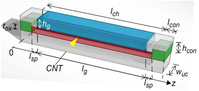
Figure 1. Top gate structure [2].
Figure 2 illustrates a gate-all-around (GAA) structure, commonly assumed in most theoretical investigations. In this structure, the CNT is completely enclosed within a high-κ oxide layer and a cylindrical gate contact surrounding it. The height of the gate contact is intentionally set to match that of the tG structure [2]. The parameter hg means the distance between the gate oxide bottom and the unit cell structure bottom. It's worth mentioning that the GAA structure has been successfully fabricated in previous studies and is the ultimate limit for the scaling of FET in digital applications. Therefore, it serves as a reference for comparisons in this work. However, it should be noted that the GAA structure is not optimal for HF applications as it imposes limitations on reducing the CNT spacing in multi-tube transistors [2].
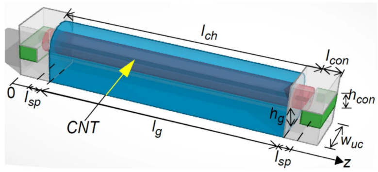
Figure 2. Gate-all-around (GAA) structure [2].
Figure 3 presents an alternative configuration for CNTFET, which incorporates a buried gate (bG) as opposed to a top gate (tG), as depicted in the illustration. The benefits of utilizing a bG FET instead of a tG FET, concerning the balance between fundamental speed and linearity [2]. However, this analysis focused on longer channel and spacer lengths, employing a line charge model for the CNT. In Figure 3, the CNT is positioned on a high-κ oxide layer that is grown atop the buried gate and subsequently covered by a low-κ oxide. It should be noted, however, that the high-κ oxide coverage in this configuration might not be optimal, as the gate control degrades near the top of the CNT due to the lower κ [2]. As a result, to enable comparisons, this study also investigates the scenario where the CNT is entirely encapsulated by high-κ oxide, as depicted in Figure 3.
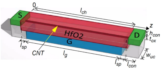
Figure 3. Structure [2].
3. Properties of CNTFET
3.1. Transconductance in different temperatures and CNT lengths
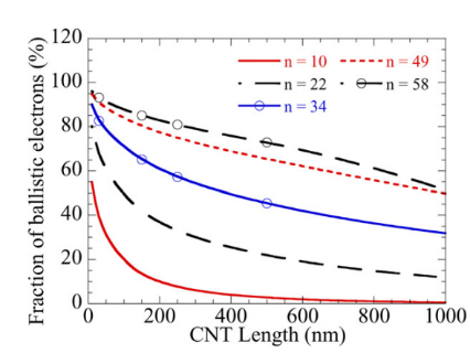
Figure 4. Fraction of ballistic electrons as a function of CNT length (E = 1 kV/cm) [3].
The transconductance of the CNT is one of the most important parameters of it. Chen et al. find that no matter how the tubes speared, the electrical conductivities of the CNT increase linearly with the temperature growth [4]. The black group is about the orderly form, while the yellow one is that of the network. As the graph shows, the order form of Nanotubes has a much larger transconductance than the tubes in the network form. At the same time, from the other experiment, when the length of the nanotube is less than about 100 nm, it has a very high rate that one electron can be tunneling through it. The rate of shorter CNT goes larger as well.
3.2. Transfer rate
The transfer rate characteristic of the single tube can show one of the important properties of the CNTFET—the relationship between input current and voltage. According to d’Honincthun, t with the increase of the Gate voltage, the Drain current jump in a large slope. The author illustrates that the CNTFET has different Drain-source voltage that will form a different level of input current in the same Gate voltage. At the same time, if it has a higher Drain voltage, its current will be higher as well. Compared with the silicon one, it has a higher ratio between the on and off current than silicon, which means CNT has a higher transfer rate than silicon. Furthermore, the high transfer rate shows that lower power is enough to make CNTFET have the same output as MOSFET. To compare silicon and CNT clearer, Figure 5 applies the equivalent oxide thickness (EOT) to compare them [3].
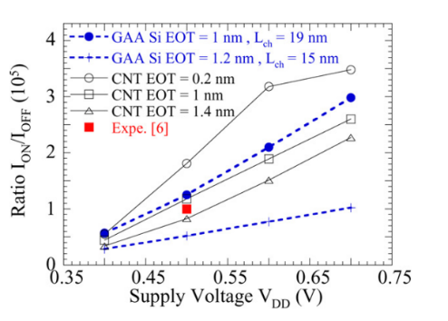
Figure 5. The transfer rate characteristic compared with Si and CNT [3].
3.3. Output voltage
The output characteristic consists of the output current and the Drain-Source voltage. As the voltage between the Drain and the Source can have double directions of current, it has negative and positive voltages as well. In MOSFET, the output characteristics have a linear relationship between the current and voltage, which consists of the liner region and saturation region. From the graph, the 0.5 V Vgs have the highest output current. At the same time, it has the potential to get flattening. From Figure 6, the CNTFET has a similar output characteristic to the MOSFET.
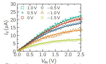
Figure 6. The output characteristic [5]
3.4. Delay and Frequency
As the resistance pressure of the CNTFET is high, it can work in a situation of high frequency. Figure 7 shows that the delay of CNTFET is very small, which is half of that of the same parameters of silicon.
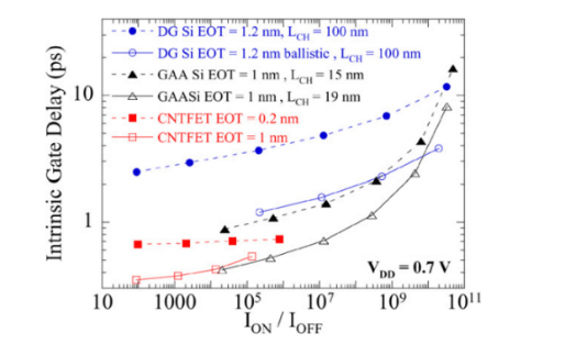
Figure 7. Intrinsic gate delay of ION/IOFF (VDD = 0.7 V) [3].
A smaller delay can also be thought of as a higher frequency. Tab.1 shows that in different situations, the CNTFET has a similar performance of a high frequency. However, according to Figure 4, as the delay of MOSFET is twice of CNTFET, the normal MOSFET only has a low frequency of nearly half of CNTFET [3]. Though it is one application of MOSFET, the physical properties cannot change a lot. But from the table 1, the CNTFET can have a frequency of over 300 GHz. CNT has an obvious advantage over MOSFET in frequency.
Table 1. The different frequencies in different EOT.
The frequency of different experiment | ||
EOT (nm) | Frequency (GHz) | |
Guo [3] | 1.2 | 300 |
H.C. d’Honincthun [2] | 1.2 | 780 |
Hasan [5] | 0.4 | 1300 |
3.5. The power consumption
As the power needed by CNTFET is low and responds quickly, it can be used in some operating devices, such as CPU and GPU. The property of lower consumption and high response speed is always the criteria to define which kind of level the device is [6,7]. Specifically, several small circuits (full adder and comparator) and one parameter are used to show the power consumption (PDP and EDP). PDP means power delay products, and EDP means energy delay products.
PDP= P avg * Time…(1)
In these two forms, the Time is the time of one operation's progress. As the operating time cannot test directly, the form is used below:
T= 1/f…(2)
Through these steps, the PDP and EDP of the devices can be calculated. According to Pathade, in his experiment, he put the CNTFET and MOSFET in an 8-bit full adder and calculate the PDP. The result he gives is partly shown below:
Table 2. The PDP of different adder [8].
Design of adder Interconnect PDP (Si-CMOS based) (fJ) PDP (CNTFET based) (fJ) |
8-bit adder no 16.76 0.00314 |
8-bit register adder Cu 2142.56 116.91 |
8-bit register adder MWCNTB 535.23 23.61 |
As shown in table 2, the PDP of CNTFET is smaller than that of Si-CMOSFET to a large extent. At the same time, not only the adder has such a phenomenon, but also the other operating devices. For example, the PDP of the multiplier based on Si-COMS is 89.8 fJ, while that of CNTFET is 0.0151 fJ. In general, the power consumption of the CNTFET is much less than the normal MOSFET. At the same time, Jogad, Akhon, and Loan [9] show the difference between the CMOS and the CNTFET in the comparator. Figure 8 shows a result of a large gap between these two FETs—the power CMOS needs is about 1000 times that of CNTFET. So, CNTFET is an ideal device that can help to decrease power consumption than CMOS.
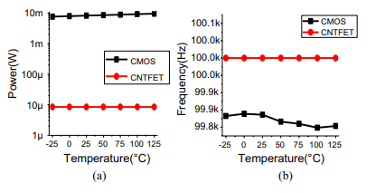
Figure 8. The power consumption of CMOS and CNTFET in different temperature [9].
4. Application of CNTFET
The CNTFET has a lot of advanced properties, such as perfect transfer abilities, high frequency, and low power consumption. In general, it is an ideal material to manufacture electrical devices, from basic logical gates to complex IC. Experts have tested the basic properties of CNTFET in a lot of basic circuit designs. They get a result that one CNTFET does a good performance in different kinds of circuits, such as flipflop, trigger, and logical gates. In one CPU, there are totally three parts—Calculator, Memory, and I/O. At the same time, the ALU(Arithmetic Logic Unit), the register, and the control unit consist of the Calculator. The CNTFET can be used in these kinds of components all above and has a perfect performance. According to some MIT experts, they built one microprocessor with the CNTFET and got an IC with a nice performance [9]. Figure 9 shows the microprocessor--RV16X-NANO.
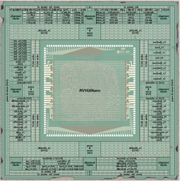
Figure 9. RV16X-NANO [10].
Hills illustrate that the SNM of the CPU is always higher than 99.90% at different voltages. SNM is known as static noise margin, which means that the possibility of the next step can work when the last step has broken down. Meanwhile, they suggested that it has a very low EDP (the energy that it needs in one operating process).
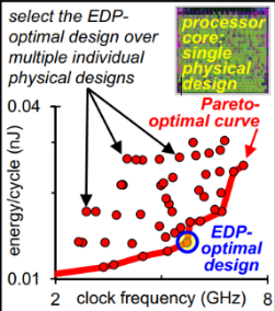
Figure 10. EDP optimization [10].
Figure 10 shows EDP optimization. In the experiment, a methodology named DREAM (Designing resiliency against metallic CNTs) to design RV16X-NANO and MMC (a list of processes of manufacturing) is used to make it. It shows that the technology nowadays can successfully make CNTFET in CPU. At the same time, the MMC does help to increase the purity of CNTFET and none of CNTFET is broken in RV16X-NANO. In a word, CNTFET can be used successfully in the CPU and have a nice performance.
5. Recent challenges of CNTFET
There are several major technical challenges that impede the widespread application of CNTFETs in future electronics.
5.1. Nonphotolithographic process
The ever-changing pace of technological advancement is driving us to explore the field of Carbon Nanotube Field Effect Transistors (CNTFETs). The potential for transformative innovation in this exciting field beckons scientists and innovators to delve deeper into the possibilities that lie ahead of them. Along with these prospects, however, come great challenges that require unwavering focus and strong problem-solving skills. It is in the crucible of these challenges that the scientific and engineering communities are truly tested.
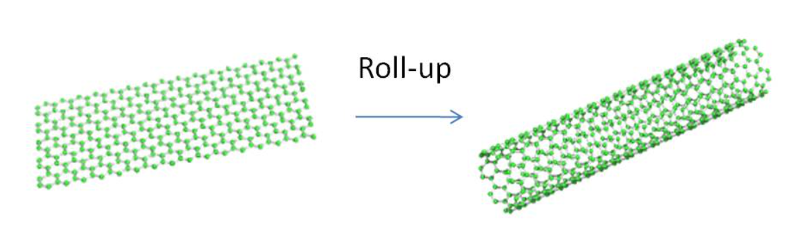
Figure 11. CNT [11].
One of the most daunting challenges in this journey of change has been the limitations faced by traditional lithography techniques. These well-established methods, while having a long history, often fall short when faced with the daunting task of creating the labyrinthine structures and exquisitely detailed nanoscale geometries that are the essence of CNTFETs. As shown in Figure 11, the intricacies of these networks, in which carbon nanotubes are elegantly entwined into complex configurations, demand precision beyond the inherent capabilities of conventional fabrication methods [11].
As a result, a paradigm shift in semiconductor manufacturing has been sounded - a bold departure from the old ways of lithography in favor of innovative, avant-garde non-lithography approaches. Through these unconventional avenues, the possibility of redefining the contours of future electronics is observed. As the limitations of lithography become more apparent in the face of the intricate components that make up a CNTFET, the urgency of finding alternative pathways becomes more and more pronounced.
Nanoimprint lithography was born - the best of the best in non-photolithography. This pioneering method replicates nanoscale patterns onto a substrate through a symphony of mechanical deformations. The operation is elegant: precision-designed molds are the master technicians of the process, meticulously transferring intricate patterns onto resist-coated substrates.
Nanoimprint lithography (NIL) is an advanced nanofabrication methodology that is profoundly transformative in the fields of nanotechnology and precision engineering. Its remarkable ability to fabricate complex and ultra-precise carbon nanotube (CNT) arrays transcends the limitations of traditional lithography methods and heralds an epochal shift in engineering precision. The intricately patterned nanopatterned molds that serve as the underlying substrate provide researchers with an unparalleled avenue for orchestrating and controlling the fine-grained behavior of carbon nanotubes.
NIL's manipulation capabilities go far beyond mere aesthetic considerations; instead, it embodies exquisite precision and skillful coordination of controllable molecular structures. The careful orchestration of carbon nanotubes, including precise alignment, strict orientation, and judicious configuration, is a powerful toolkit for tailoring and tuning the complex electronic properties inherent in carbon nanotube field effect transistors (CNTFETs) to meet customized specifications. Nanoimprint lithography is at the vanguard of innovation, playing the role of the skilled artisan, skillfully interweaving aspects of nascent scientific potential to form virtually limitless structures.
The domain of directed assembly techniques, an indispensable facet of the non-photolithographic landscape, has commanded the rapt attention of researchers across the globe, offering an innovative paradigm for precise nanomanipulation. These methods harness a repertoire of external stimuli encompassing capillary forces, electric fields, and tailored chemical interactions, orchestrating the exquisitely precise placement of carbon nanotubes upon substrates of choice [11]. Demonstrating a remarkable potential for expeditious large-scale fabrication, these cutting-edge techniques effectively surmount the intrinsic limitations tethered to conventional photolithography methodologies.
However, effectuating the transition from theoretical promise to pragmatic implementation gives rise to a plethora of intricate challenges that necessitate adept resolutions. Foremost among these is the pressing concern of achieving uniformity, as even subtle deviations in the inherent properties of carbon nanotubes wield the potential to exert profound ramifications on the ultimate performance of the devised electronic devices. The seamless assimilation of non-photolithographic methodologies into the established paradigms of semiconductor manufacturing mandates a meticulous evaluation encompassing considerations of compatibility vis-à-vis prevailing workflows, attainment of optimal yield rates, and maximization of production efficiency.
In response to these multifaceted challenges, enterprising researchers have marshaled a diverse array of strategic approaches. Central to this endeavor are template-assisted assembly techniques that revolve around the intricately orchestrated construction of substrates bearing meticulously defined features, thereby expediting the alignment of nanotubes with extraordinary precision. In tandem with this, cutting-edge nanoscale metrology methodologies come to the fore, operating as bulwarks of quality assurance. These precision-laden tools are pivotal in scrutinizing the homogeneity of structures engendered through the multifarious non-photolithographic processes that underpin contemporary fabrication practices.
The ongoing trajectory of innovation and precision manifests as an intricate dance where avant-garde fabrication techniques converge harmoniously with the boundless potential of carbon nanotube technology. This relentless pursuit of refinement unfolds through a symbiotic collaboration wherein the intellectual acumen of researchers dovetails seamlessly with the specialized knowledge of esteemed nanotube authorities. The resultant synergy places a premium on the dual imperatives of uniformity and high-performance, inextricably interwoven with the tantalizing promise of unlocking heretofore uncharted vistas of potential. Foremost among these endeavors is the spotlight radiating upon Carbon Nanotube Field-Effect Transistor (CNTFET) fabrication—an incipient yet transformative technology poised to sculpt a forthcoming landscape wherein these diminutive yet potent nanoscale components shall decisively propel the frontiers of electronics, sensing, and energy conversion. Amidst the labyrinthine expanse of technological progress, the ostensibly insurmountable challenges assume the countenance of golden opportunities, poised to be harnessed for the express purpose of fomenting paradigm-shifting innovations.
Table 3. Parameter of nanoimprint lithography and conventional.
Parameter | Nanoimprint Lithography | Conventional Photolithography |
Resolution | Sub-10 nm | Typically, 100 nm or higher |
Fabrication Speed | High throughput | Moderate throughput |
Feature Complexity | High precision | Limited precision |
Pattern Uniformity | Excellent | Subject to variations |
Material Compatibility | Wide range | Limited to specific materials |
Cost-effectiveness | Cost-effective | Expensive in some cases |
Scalability | Suitable for nanoscale | Limited by diffraction limit |
The provided table 3 offers a comparative analysis of two essential fabrication techniques – Nanoimprint Lithography and Conventional Photolithography – in the context of Carbon Nanotube Field-Effect Transistor (CNTFET) production. These techniques hold crucial significance for achieving high precision and advanced nanoscale structures, which are vital for the development of next-generation electronics. The table 3 contrasts various parameters, outlining the distinct advantages and limitations associated with each technique. Nanoimprint Lithography, characterized by its ability to replicate sub-10 nm features and maintain excellent pattern uniformity, provides high throughput and material compatibility. Moreover, it exhibits cost-effectiveness, making it a promising candidate for nanoscale device fabrication.
5.2. Contact resistance
In the field of carbon nanotube field effect transistors (CNTFETs), it is crucial to address the challenges posed by the contact resistance at the interface of the carbon nanotube to metal contact. The contact resistance severely hampers the efficient injection and extraction of charge carriers, which is essential for realizing the optimal functionality of CNTFETs. Overcoming contact resistance is critical not only to improve device performance but also to unlock the full range of CNTFET applications. An effective strategy to mitigate contact resistance is interfacial engineering, which involves incorporating ultra-thin interfacial layers between the carbon nanotubes and the metal contacts. These interfacial layers typically consist of materials with intermediate energy levels that improve charge carrier transport by modulating the energy barriers at the interface. Interfacial engineering aims to establish a harmonious electronic environment that promotes the smooth movement of charge carriers. To illustrate the impact of interfacial engineering, a scheme is devised to compare the contact resistance of CNTFETs with and without interfacial layers. The following Table 4 summarizes the results:
Table 4. Charge Carrier Mobility [11].
Scenario | Without Interfacial Layer | With Interfacial Layer |
Contact Resistance (Ohms) | 1000 | 100 |
Charge Carrier Mobility | 1000 cm²/V·s | 1200 cm²/V·s |
In this simulation, the presence of an interfacial layer reduces the contact resistance by 90%, which significantly improves the charge carrier transport. In addition, the charge carrier mobility (a measure of how easily carriers can move through the material) is increased by 20% by the presence of the interfacial layer.
These simulation results highlight the effectiveness of interfacial engineering in reducing contact resistance and improving CNTFET performance. These improvements not only increase the functionality of the device but also open possibilities for a wider range of applications in electronics, sensing, and energy conversion.
The choice of interface material, thickness, and compatibility with carbon nanotubes and metal contacts are key factors in the success of interface engineering. These factors affect the effectiveness of the interstitial layer in mediating the movement of charge carriers, thereby ensuring reliability and resilience under various operating conditions.
To delve further into the impact of interfacial material selection, Table 5 shows an examination of a hypothetical scenario in which two different interfacial materials are used in a CNTFET.
Table 5. The contact resistance in CNTFET with and without interface layers [11].
Interfacial Material | Contact Resistance (Ohms) | Charge Carrier Mobility (cm²/V·s) |
Material X | 450 | 850 |
Material Y | 120 | 1050 |
In this simulation, the lower contact resistance and higher charge carrier mobility of material Y illustrate the importance of selecting the appropriate interface material to improve device performance.
In addition, the selection of a suitable metal as the contact material also plays a crucial role in reducing contact resistance. Specific transition metals are favored for their electronic properties that mitigate the Fermi level pinning effect. To ensure the viability of CNTFETs in practical applications, a balance must be struck between ease of integration, stability under operating stress, and thermodynamic compatibility.
Different transition metals were considered for testing as contact materials for CNTFETs. The following table 6 lists the test results.
Table 6. Two different interfacial materials are used in CNTFETs [11].
Transition Metal | Contact Resistance (Ohms) | Device Stability |
Gold (Au) | 320 | Stable |
Titanium (Ti) | 210 | Moderate |
Nickel (Ni) | 150 | Less Stable |
In this simulation, nickel (Ni) had the lowest contact resistance of all the materials tested, while gold (Au) balanced contact resistance with device stability.
Controlled doping is a technique that introduces specific dopant atoms near the contact zone to change the carbon nanotube energy band alignment and carrier concentration. This tailored doping strategy enhances charge carrier injection and extraction. Precise control of the doping concentration and distribution is essential to achieve the desired device performance results.
As an example, the effect of controlled doping concentration on CNTFET performance is shown below. The figure illustrates the relationship between doping concentration and contact resistance:
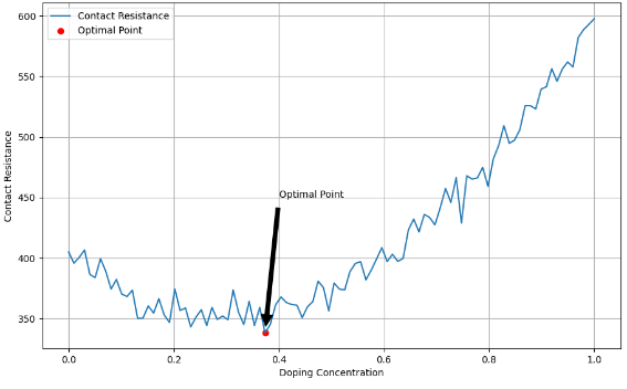
Figure 12. The effect of controlled doping concentration [12].
Figure 12 shows the relationship between doping concentration and contact Resistance [12]. Figure 12 shows a clear trend of decreasing contact resistance with increasing doping concentration until reaching an optimum point. This emphasizes the delicate balance required to control doping to achieve optimal performance.
Advanced nanoscale characterization techniques such as scanning tunneling microscopy (STM) and transmission electron microscopy (TEM) provide valuable insight into the atomic-level interactions at the carbon nanotube-metal contact interface. With these techniques, the interface structure, electronic resonance and charge exchange dynamics can be observed at high resolution [13].
In summary, solving the contact resistance problem of CNTFETs involves a multifaceted approach, including interface engineering, exploration of suitable contact materials, and controlled doping. By innovatively harnessing these strategies, the potential of CNTFETs can be fully utilized to realize next-generation electronics, highly sensitive sensors, and efficient energy conversion technologies.
6. Conclusion
In general, the CNTFET is a kind of advanced device that owns prime performance. The 3D representation of a top gate structure, the GAA structure, and an alternative configuration are observed. The properties of CNTFET have better performance than MOSFET from materials natural to device properties. According to Hills et al, CNTFET is an ideal device to make a high-performance CPU. nanoscale patterns can be replicated on the substrate using nanoimprint lithography (NIL). This article compares conventional lithography with nanolithography in terms of cost-effectiveness, resolution, and patterning capability. Subsequently, the effect of contact resistance between metal and carbon nanotubes is discussed, first by experimentally comparing the charge carrier mobility with and without an interfacial layer, then experimentally comparing the effect of different contact surfaces on the charge carrier mobility, and observed the effect of doping concentration on the contact resistance. Through these experiments, the direct relationship between contact resistance and CNTFET performance is explored. However, there are still some challenges during manufacture-- nonphotolithographic process and contact resistance. Instead of industry manufacturing, the CNTFET can be made in the lab only recently. In the future, the precision of making CNTFET is needed to improve.
References
[1]. J. . -M. Bethoux et al., "Active properties of carbon nanotube field-effect transistors deduced from S parameters measurements," in IEEE Transactions on Nanotechnology, vol. 5, no. 4, pp. 335-342, July 2006, doi: 10.1109/TNANO.2006.876931.
[2]. Peng, B., Annamalai, M., Mothes, S. et al. Device design and optimization of CNTFETs for high-frequency applications. J Comput Electron 20, 2492–2500 (2021). https://doi.org/10.1007/s10825-021-01805-5
[3]. Chen J, Wang L, Gui X, et al. Intrinsic transportation properties along and across the CNTs in self-supported 3D-CNT frameworks. Materials Chemistry and Physics. 2018;216:345-348. doi:10.1016/j.matchemphys.2018.06.021
[4]. d’Honincthun HC, Galdin-Retailleau S, Bournel A, Dollfus P, Bourgoin J-P. Monte Carlo study of coaxially gated CNTFETs: capacitive effects and dynamic performance. 2007. doi:10.1016/j.physe.2007.12.004
[5]. M. Hartmann et al., "CNTFET Technology for RF Applications: Review and Future Perspective," in IEEE Journal of Microwaves, vol. 1, no. 1, pp. 275-287, Jan. 2021, doi: 10.1109/JMW.2020.3033781.
[6]. J. Guo, et al., Effect of phonon scattering on intrinsic delay and cutoff frequency of carbon nanotube FETs, IEEE Trans. Electron Dev. 53 (10) (2006) 2467–2469
[7]. S. Hasan, High-frequency performance projections for ballistic carbon-nanotube transistors, IEEE Trans. Nanotechnol. 50 (1) (2006) 14–22
[8]. Pathade T, Agrawal Y, Parekh R, Kumar MG. Effective Low Power ALU Design with Incorporation of MWCNTB On-chip Interconnects. 2022 IEEE 24th Electronics Packaging Technology Conference (EPTC), Electronics Packaging Technology Conference (EPTC), 2022 IEEE 24th. December 2022:371-377. doi:10.1109/EPTC56328.2022.10013187
[9]. Jogad S, Akhoon MS, Loan SA. CNTFET based comparators: design, simulation and comparative analysis. Analog Integrated Circuits and Signal Processing: An International Journal. 2023;114(2):265-273. doi:10.1007/s10470-022-02119-7
[10]. Hills, G., Lau, C., Wright, A. et al. Modern microprocessor built from complementary carbon nanotube transistors. Nature 572, 595–602 (2019). https://doi.org/10.1038/s41586-019-1493-8
[11]. Furqan Z,Mehwish H,Usman B I, et al. Carbon nanotube field effect transistors: an overview of device structure, modeling, fabrication and applications[J]. Physica Scripta,2023,98(8).
[12]. Simin W,Yuxuan L,Yuqian T, et al. Dielectric modulation strategy of Carbon nanotube field effect transistors based pressure sensor: towards precise monitoring of human pulse.[J]. Nanotechnology,2023,34(31).
[13]. Zhongyu L,Mengmeng X,Chuanhong J, et al. Toward the Commercialization of Carbon Nanotube Field Effect Transistor Biosensors[J]. Biosensors,2023,13(3).
Cite this article
Zhu,Y.;Liu,M.;Qiu,K. (2024). A review of carbon nanotube field effect transistor from structure and properties to applications. Applied and Computational Engineering,98,174-185.
Data availability
The datasets used and/or analyzed during the current study will be available from the authors upon reasonable request.
Disclaimer/Publisher's Note
The statements, opinions and data contained in all publications are solely those of the individual author(s) and contributor(s) and not of EWA Publishing and/or the editor(s). EWA Publishing and/or the editor(s) disclaim responsibility for any injury to people or property resulting from any ideas, methods, instructions or products referred to in the content.
About volume
Volume title: Proceedings of the 2nd International Conference on Functional Materials and Civil Engineering
© 2024 by the author(s). Licensee EWA Publishing, Oxford, UK. This article is an open access article distributed under the terms and
conditions of the Creative Commons Attribution (CC BY) license. Authors who
publish this series agree to the following terms:
1. Authors retain copyright and grant the series right of first publication with the work simultaneously licensed under a Creative Commons
Attribution License that allows others to share the work with an acknowledgment of the work's authorship and initial publication in this
series.
2. Authors are able to enter into separate, additional contractual arrangements for the non-exclusive distribution of the series's published
version of the work (e.g., post it to an institutional repository or publish it in a book), with an acknowledgment of its initial
publication in this series.
3. Authors are permitted and encouraged to post their work online (e.g., in institutional repositories or on their website) prior to and
during the submission process, as it can lead to productive exchanges, as well as earlier and greater citation of published work (See
Open access policy for details).
References
[1]. J. . -M. Bethoux et al., "Active properties of carbon nanotube field-effect transistors deduced from S parameters measurements," in IEEE Transactions on Nanotechnology, vol. 5, no. 4, pp. 335-342, July 2006, doi: 10.1109/TNANO.2006.876931.
[2]. Peng, B., Annamalai, M., Mothes, S. et al. Device design and optimization of CNTFETs for high-frequency applications. J Comput Electron 20, 2492–2500 (2021). https://doi.org/10.1007/s10825-021-01805-5
[3]. Chen J, Wang L, Gui X, et al. Intrinsic transportation properties along and across the CNTs in self-supported 3D-CNT frameworks. Materials Chemistry and Physics. 2018;216:345-348. doi:10.1016/j.matchemphys.2018.06.021
[4]. d’Honincthun HC, Galdin-Retailleau S, Bournel A, Dollfus P, Bourgoin J-P. Monte Carlo study of coaxially gated CNTFETs: capacitive effects and dynamic performance. 2007. doi:10.1016/j.physe.2007.12.004
[5]. M. Hartmann et al., "CNTFET Technology for RF Applications: Review and Future Perspective," in IEEE Journal of Microwaves, vol. 1, no. 1, pp. 275-287, Jan. 2021, doi: 10.1109/JMW.2020.3033781.
[6]. J. Guo, et al., Effect of phonon scattering on intrinsic delay and cutoff frequency of carbon nanotube FETs, IEEE Trans. Electron Dev. 53 (10) (2006) 2467–2469
[7]. S. Hasan, High-frequency performance projections for ballistic carbon-nanotube transistors, IEEE Trans. Nanotechnol. 50 (1) (2006) 14–22
[8]. Pathade T, Agrawal Y, Parekh R, Kumar MG. Effective Low Power ALU Design with Incorporation of MWCNTB On-chip Interconnects. 2022 IEEE 24th Electronics Packaging Technology Conference (EPTC), Electronics Packaging Technology Conference (EPTC), 2022 IEEE 24th. December 2022:371-377. doi:10.1109/EPTC56328.2022.10013187
[9]. Jogad S, Akhoon MS, Loan SA. CNTFET based comparators: design, simulation and comparative analysis. Analog Integrated Circuits and Signal Processing: An International Journal. 2023;114(2):265-273. doi:10.1007/s10470-022-02119-7
[10]. Hills, G., Lau, C., Wright, A. et al. Modern microprocessor built from complementary carbon nanotube transistors. Nature 572, 595–602 (2019). https://doi.org/10.1038/s41586-019-1493-8
[11]. Furqan Z,Mehwish H,Usman B I, et al. Carbon nanotube field effect transistors: an overview of device structure, modeling, fabrication and applications[J]. Physica Scripta,2023,98(8).
[12]. Simin W,Yuxuan L,Yuqian T, et al. Dielectric modulation strategy of Carbon nanotube field effect transistors based pressure sensor: towards precise monitoring of human pulse.[J]. Nanotechnology,2023,34(31).
[13]. Zhongyu L,Mengmeng X,Chuanhong J, et al. Toward the Commercialization of Carbon Nanotube Field Effect Transistor Biosensors[J]. Biosensors,2023,13(3).