


1. Introduction
Operational amplifiers are fundamental components in various applications, including analog, digital, and mixed-signal circuits. They serve as crucial building blocks for ADCs (analog-to-digital converters), DACs (digital-to-analog converters), signal processing systems and automatic control systems etc. Additionally, they are essential for higher-order active filters, signal amplification, and ultra-high-speed signal conversion [1]. The overall performance of integrated circuits incorporating operational amplifiers heavily relies on the capabilities of these amplifiers.
An ideal operational amplifier should provide infinite bandwidth, infinite input impedance, infinite open-loop gain, infinite output voltage swing, infinite swing rate, infinite common-mode rejection ratio (CMRR), infinite power supply rejection ratio (PSRR), zero output impedance, and other characteristics.
In reality, however, the ideal operational amplifier does not exist due to manufacturing process deviations, parasitic effects, noise, and non-ideal characteristics of semiconductor devices. These realistic problems affect the performance of the amplifier, making it difficult to combine the various performances of operational amplifiers.
Therefore, when designing operational amplifiers, these non-ideal characteristics need to be taken into account. According to the actual needs of the applied scenarios, the appropriate performance indexes should be selected. The indexes should be designed with a balance and appropriate compensation and optimization.
The single-stage operational amplifier's input transistor produces a small signal current that flows directly through the output impedance, only one voltage-to-current conversion is performed. As a result, the gain of a single-stage amplifier is constrained by the product of the transconductance of the input transistors and the output impedance. While implementing a cascode structure can enhance the gain, it also limits the output swing [2]. Design of multistage operational amplifiers is more complicated. It introduces multiple poles and zeros, making compensation techniques difficult to design for high speeds and large bandwidths. Its other disadvantages include higher power consumption, larger circuit size and interference effects.
Overall, the two-stage operational amplifier structure offers a compromise. It is more widely used than single and multistage structures, due to its relatively simple structure and better performance parameters.
In some past researches, Y. Yang et al. introduced an efficient and optimized design approach for two-stage Miller-compensated operational amplifiers. They employed a neural network model to capture the relationship between op-amp parameters and performance metrics, significantly enhancing simulation efficiency [3]. C.Krithika et al. designed and simulated a high-performance CMOS two-stage amplifier using an improved Miller-compensated methodology, which was carried out in the 90nm simulation design environment of Cadence tool software. Achieved 194MHz unity-gain bandwidth, 10.8V/μS slew rate, 76dB gain and 106.3μW low power consumption and 70° phase margin [4]. Y. R. Gandweed et al. used a power gating technique to optimize the problem of high-power consumption of the two-stage operational amplifier. Two additional head transistors are connected in parallel in the circuit. The power supply to the amplifier can be turned off when the amplifier is not in use, such as during idle periods or when the input signal voltage falls below a threshold value [5]. X. Jin and J. He designed a two-stage differential op-amp using a 180nm CMOS process. It achieves a gain of 85.5dB, CMRR and PSRR are both approximately 90dB, and a Miller compensation is used to achieve a phase margin of 80° [6]. M. A. Chaudhry designed an operational amplifier operating at 0.8V single supply with 0.12μm process technology, which uses a folded cascode design to optimize the output signal voltage swing at low VDD [7].
This paper describes in detail the principle, structure, and design method of CMOS two-stage operational amplifier. It particularly focuses on the principle of stability optimization using Miller compensation and nulling resistor. The study presents the design of a Miller-compensated two-stage operational amplifier that has a high unity-gain bandwidth and demonstration of performance parameters obtained through simulation and analysis. Finally, the study concludes with a summary of the designed CMOS two-stage operational amplifier is summarized.
2. Theoretical Analysis
This section contains a theoretical analysis of two-stage operational amplifiers. It includes the function of each component, and the theory needed in the design.
2.1. Two-stage operational amplifiers
A Miller compensated two-stage op-amp is a widely used circuit structure designed to achieve high gain and better phase margins in the design of amplifiers [8]. A two-stage op-amp consists of two amplifiers cascaded together. The first stage of the circuit is a differential amplifier that delivers high gain, while the second stage is a common-source amplifier responsible for providing a wide output swing.
Two-stage op-amp achieves good balance between high gain, large output swing and bandwidth. Figure 1 shows the circuit structure of a typical two-stage operational amplifier. The transistors \( {M_{1}}~{M_{5}} \) consist a differential amplifier as first stage, \( {M_{1}} {M_{2}} \) provides the differential input to the op-amp, and this differential structure provides better suppression of common-mode disturbances. \( {M_{3}} {M_{4}} \) is a current-mirror active load, and \( {M_{5}} \) is a tail-current source providing a stable current bias to the first stage. The second stage is a common source amplifier consisting of transistors \( {M_{6}} {M_{7}} \) . The current source and \( {M_{0}} \) form a bias circuit and the current flows through the diode connected \( {M_{8}} \) to generate a bias voltage at the gate.
Signals from the first stage are fed into the second stage, which is amplified by M6. Miller capacitor \( {C_{C}} \) and nulling resistor \( {R_{C}} \) are connected with the output node of the first stage and second stage as a compensation circuit for adjusting the zero pole to improve stability. \( {C_{L}} \) is used as the output capacitance load of the op-amp.
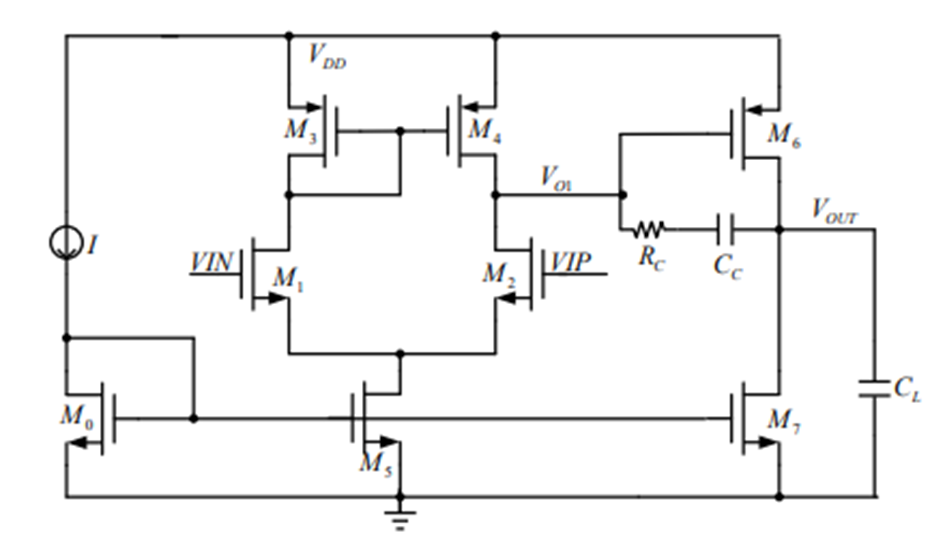
Figure 1. Two-stage operational amplifier schematic.
2.2. Design methodology
The design process for an operational amplifier involves translating performance requirements into a specific topology structure, transistor size and compensation method. The structure of the operational amplifier is firstly chosen based on the key performance criteria. Then the schematic of circuit with all transistor connections are drawn. Next, the aspect ratio of each transistor in the operational amplifier is calculated manually after clarifying the relevant process parameters. Finally, simulation is carried out by using the software, and adjustments are made according to the results. A two-stage amplifier structure has been selected for this study. A series of performance specifications are given below in relation to the parameters.
The formula for gain is shown in (1), the first stage gain \( {{A_{v}}_{1}} \) multiplied by the second stage gain \( {{A_{v}}_{2}} \) is the total gain \( {A_{v}} \) , which is the gain of the two stages as in formula. Equation (2) is the formula for the unity-gain bandwidth, reflecting the frequency when the amplifier gain is reduced to 0dB. Equation (3) is the relationship that needs to be satisfied in order to meet a phase margin greater than 60°.
\( {A_{v}}={A_{{v_{1}}}}{A_{{v_{2}}}}=\frac{{g_{m1}}{g_{m6}}}{({g_{ds2}}+{g_{ds4}})({g_{ds6}}+{g_{ds7}})} \) (1)
\( GB=\frac{{g_{m1}}}{{C_{C}}} \) (2)
\( {C_{c}} \gt 0.22{C_{L}} \) (3)
The transfer function of the two-stage op-amp that is uncompensated has two poles and the frequency positions of the poles are located before the unity-gain bandwidth is reached. In addition, the presence of multiple poles in a circuit can led to instability. So, uncompensated two-stage op-amps typically have a phase margin of less than 40°. In order to improve stability, the phase margin of the op-amp should be at least greater than 45° and preferably greater than 60°. Therefore, it is crucial to introduce frequency compensation circuits into operational amplifiers to ensure their stable operation at all operating conditions. In this design, the Miller effect is used for pole separation.
Figure 2 shows the distribution of zero poles before and after compensation, figure 3 shows the baud plot before and after compensation [9], equations (4) ~ (6) are the zero poles after Miller compensation, and the equations reflect the relationship between \( {C_{C}} \) and the position of zero poles. Combining the amplitude-frequency curve and phase frequency curve in the baud plot, it can be seen that after Miller compensation, the original two poles \( {{p_{1}}^{ \prime }} \) and \( {{p_{2}}^{ \prime }} \) are separated to both sides and moved to the positions of \( {p_{1}} \) and \( {p_{2}} \) , while the zero \( {z_{1}} \) is introduced.
*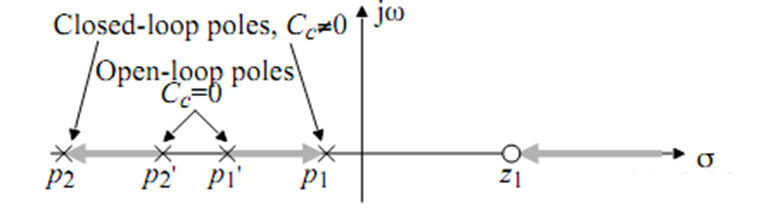
Figure 2. Comparison of zero poles before and after compensation [9].
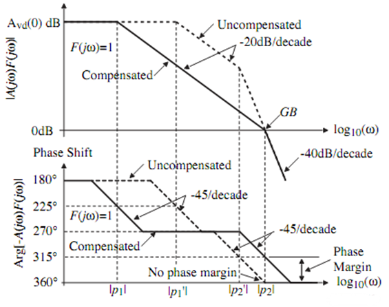
Figure 3. Baud plot before and after compensation [9].
\( {z_{1}}=\frac{{g_{mII}}}{{C_{C}}}=\frac{{g_{m6}}}{{C_{C}}} \) (4)
\( {p_{1}}≅\frac{-1}{{g_{mII}}{R_{I}}{R_{II}}{C_{C}}}≅\frac{-({g_{ds2}}+{g_{ds4}})({g_{ds6}}+{g_{ds7}})}{{g_{m6}}{C_{C}}} \) (5)
\( {p_{2}}≅\frac{-{g_{mII}}{C_{C}}}{{C_{I}}{C_{II}}+{C_{C}}{C_{I}}+{C_{C}}{C_{II}}}≅\frac{-{g_{m6}}}{{C_{L}}} \) (6)
While applying Miller compensation, due to the presence of Miller capacitance, there are two feedforward paths at the output node. At a certain complex frequency, if the signals passing through these two paths are equal in magnitude but opposite in phase, they cancel each other out. This cancellation introduces a RHP (right half-plane) zero \( {z_{1}} \) . The zero \( {z_{1}} \) has no direct effect on system stability, but the system may become unstable due to the position of the two poles as the phase lag due to this pole reduces the phase margin. To eliminate the RHP zero, the use of a nulling resistor needs to be considered. A nulling resistor \( {R_{z}} \) , is connected in series with the branch on which the Miller compensation capacitor is located. The nulling resistor introduces a weaker third pole in the system, but it is able to push the RHP zero away from the main pole of the system. The positions of pole \( {p_{1}} \) and pole \( {p_{1}} \) remain almost constant [10]. The expressions for the zero \( {z_{1}} \) and pole \( {p_{3}} \) are shown by equations (7) and (8).
\( {z_{1}}=\frac{1}{{C_{C}}(\frac{1}{{g_{mII}}}-{R_{Z}})} \) (7)
\( {p_{3}}=-{g_{mII}}(\frac{1}{{C_{I}}}+\frac{1}{{C_{C}}}+\frac{1}{{C_{L}}}) \) (8)
It is easy to see that the position of the zero \( {z_{1}} \) can be moved by adjusting the value of \( {R_{z}} \) . Typically, to eliminate the effect of RHP, adjusting \( {R_{z}} \) moves the RHP zero farther away than \( GB \) , or to a position \( {p_{2}} \) with respect to the load capacitance with the poles cancelled out.
3. Simulation
Table 1 shows the design requirements of the op-amp in this design, where the required supply voltage is 3.3V, the unity-gain bandwidth should be more than 800MHz, the gain is more than 60dB, and the phase margin is more than 60°. The schematic diagram of the two-stage operational amplifier designed and drawn with Cadence software using the 180 nm CMOS process is shown in figure 4.
Table 1. Operational amplifier design requirements.
Performance parameters | Performance requirements |
ICMR | 3V |
Power consumption | ≤20mW |
Gain | ≥60dB |
GB | ≥800MHz |
Phase margin | ≥60° |
CMRR | ≥60dB |
PSRR | ≥70dB |
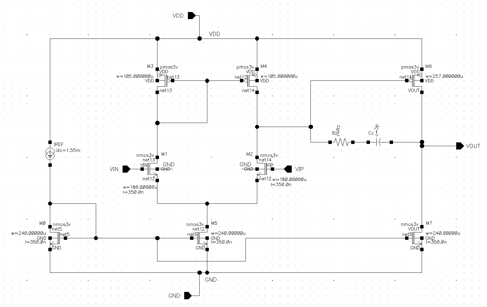
Figure 4. Schematic of designed two-stage amplifier.
3.1. DC analysis
The DC analysis includes ICMR and output swing. To test the ICMR, the operational amplifier is configured in a unity-gain feedback loop as figure 5. The voltage input in the positive input terminal is swept from 0V to VDD while observing the output voltage response. The linear range can be observed from the output voltage versus input voltage curve. In the linear operating region of the amplifier, the slope of the DC sweep curve is 45°, indicating that the output can effectively follow the input. If the input exceeds the linear range, the curve bends. The final simulation results are shown in figure 6, where the boundary points of the linear region are identified. The simulation concludes that the ICMR is 3.102V.
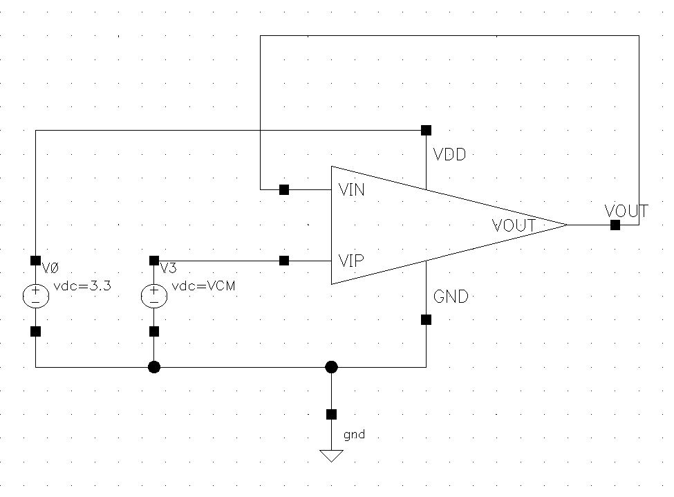
Figure 5. ICMR test circuit.
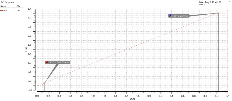
Figure 6. ICMR test result.
To test the swing, the designed amplifier is connected to the structure shown in figure 7, which voltage gain is -10. The positive input of the op-amp is connected to VDD/2 to provide the op-amp with a common-mode input in the center of power supply rails, and a DC sweep from 0 to VDD is performed on the negative input, and the portion of the output voltage that varies linearly is the swing under this power condition. The result of the voltage swing is obtained as shown in figure 8, which gives the swing range: 317.075mV-3.00137V.
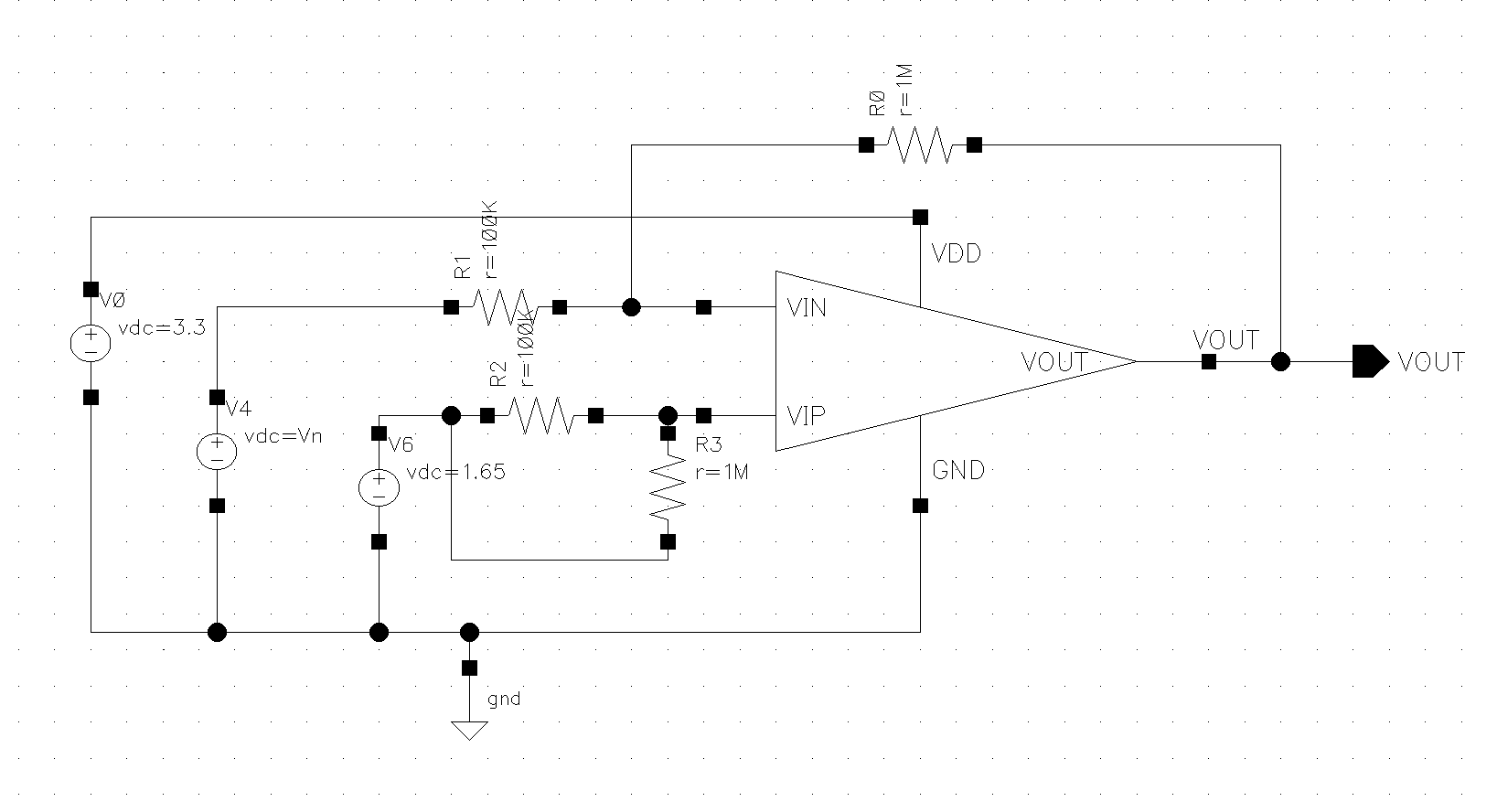
Figure 7. Swing test circuit.
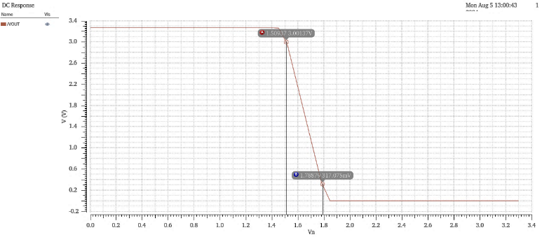
Figure 8. Swing test result.
3.2. AC Analysis
AC analysis mainly tests frequency-related parameters, including gain, GB, phase margin, CMRR and PSRR.
3.2.1. Open loop frequency response
Due to the op-amp has a very high open-loop gain, the circuit is very sensitive to adaptation, making it difficult to measure the gain using an open-loop method directly. Therefore, common-mode feedback is applied to stabilize the output voltage of common-mode stage. The test circuit, as shown in figure 9, is designed as a practical circuit for measuring the open-loop AC parameters.
In the test circuit, the resistor (R0) and capacitor (C2) form a low-pass feedback network with very large values, ensuring that the cutoff frequency is much lower than the operational amplifier's dominant pole frequency. This configuration makes the DC levels of the positive and negative input terminals equal, with the negative input terminal AC-grounded. CL represents the expected load for the operational amplifier. A sinusoidal input signal with a magnitude of 1V, and an AC sweep is performed over a frequency range of 0.1Hz to 10GHz. The test results, as shown in figure 10, indicate that the operational amplifier has a GB of 907.42MHz, a phase margin of 75.02°, and a gain of 61.80dB.
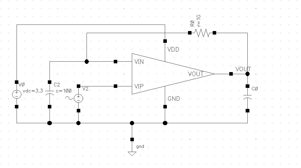
Figure 9. Frequency response test circuit.
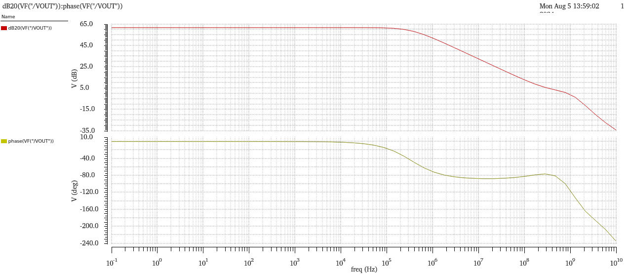
Figure 10. Amplitude-frequency and phase-frequency curves.
3.2.2. CMRR
Figure 11 shows the CMRR test circuit, the op-amp is connected as a unit negative feedback structure, a unit AC small signal source vcm is added between the output and the negative input, and the same signal is added to the positive input; the VCM provides the circuit with a DC operating point, and the CMRR can be obtained by performing an AC frequency sweep of the structure as shown in figure 11, and the CMRR of this op-amp is about As shown in figure 12, the CMRR of this designed op-amp is about 60.44dB.
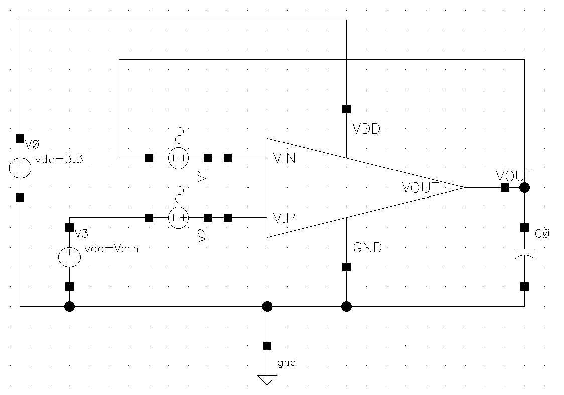
Figure 11. CMRR test circuit.
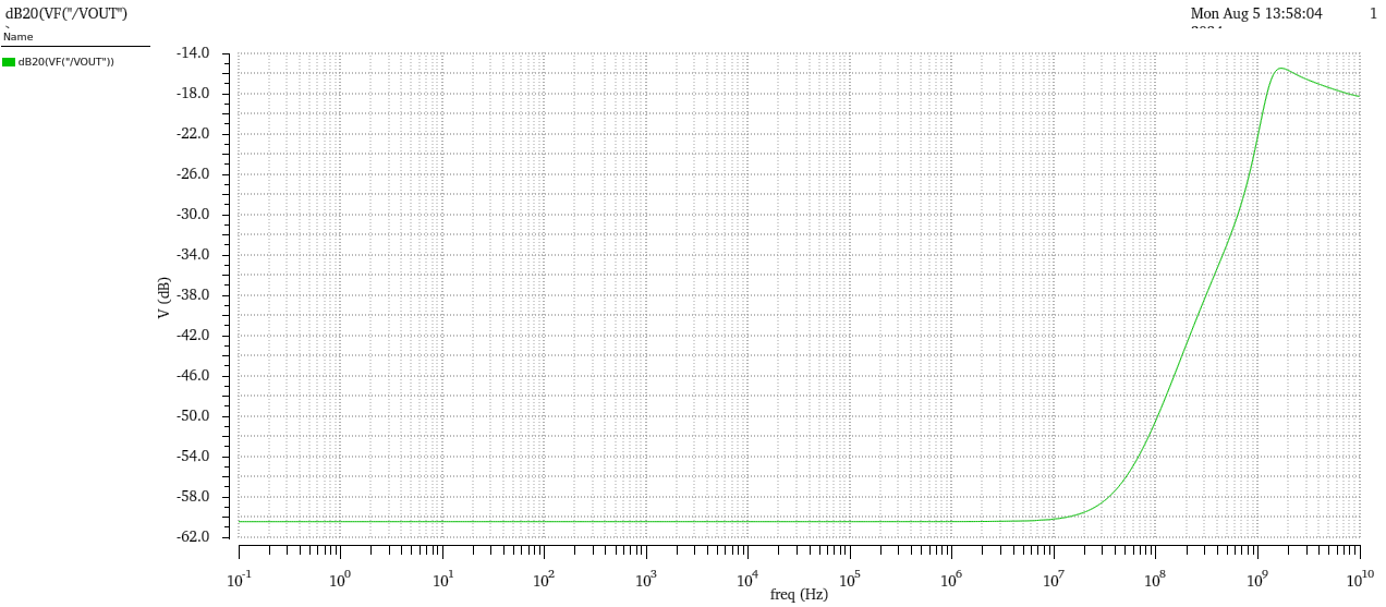
Figure 12. CMRR test result.
3.2.3. PSRR
Figure 13 shows the PSRR test circuit, which is similar to the simulation of CMRR, connecting the op-amp into the form of a unit of negative feedback, and adding a unit of AC component to the supply voltage, performing AC frequency scanning, and observing the frequency response of the output to obtain PSRR, and the test results are shown in figure 14, with a PSRR of about 70.01dB.
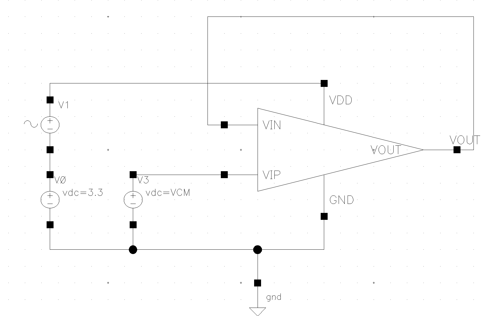
Figure 13. PSRR test circuit
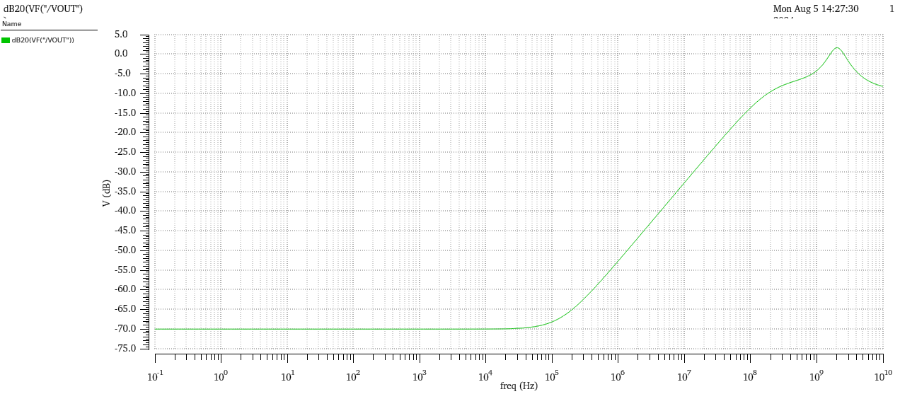
Figure 14. PSRR test result
3.3. Results
Table 2. Comparison of simulation results and performance requirements.
Performance Parameters | Performance Requirements | Simulation Results |
ICMR | 3V | 3.102V |
Power Consumption | ≤20mW | 15.53mW |
Gain | ≥60dB | 61.80dB |
GB | ≥800MHz | 907.42MHz |
Phase Margin | ≥60° | 75.02° |
CMRR | ≥60dB | 60.44dB |
PSRR | ≥70dB | 70.01dB |
Table 2 shows that the amplifier of this design achieves better-than-designed performance in terms of common-mode input range, swing, gain, unity-gain bandwidth, phase margin, CMRR, and PSRR.
4. Conclusion
In this paper, based on the application of operational amplifiers, the research background, principle, design, and simulation and verification methods of two-stage operational amplifiers are described in detail. And a two-stage op-amp with 907.42MHz high unity-gain bandwidth is designed and simulated using Cadence Virtuoso tool in 180nm CMOS process to improve the unity-gain bandwidth by varying the width of the transistors, and increasing the current. Bandwidth and stability related issues are improved by nulling resistors and Miller capacitors. Successfully realized a two-stage op-amp that is better than the design requirements.
In future research, new circuit topologies, compensation means and more efficient design methods can be explored to further optimize and improve the performance metrics such as gain, bandwidth, power consumption, stability, and the balance between them.
References
[1]. Thulasi Y Krishna K L Reddy D Srinivasulu Hemanthi V Reddy T B and Lalithapriya T 2023 An Improved Miller Compensated Two Stage CMOS Operational Amplifier 2023 Second International Conference on Electronics and Renewable Systems (ICEARS) Tuticorin India pp 332-336
[2]. Razavi B 2017 Design of Analog CMOS Integrated Circuits 2nd ed New York NY USA McGraw-Hill Educ pp 1-780
[3]. Yang Y Yin X Chen D Li D and Yang Y 2024 The High-Efficiency Optimization Design Method for Two-Stage Miller Compensated Operational Amplifier IEEE Transactions on Circuits and Systems II Express Briefs vol 71 no 4 pp 2029-2033
[4]. Krithika C Krishna K L Reddy D Srinivasulu Lakshmi B G Bhaskar K M and Vijay Sai K G 2024 Implementation of a Compensated Two-Stage Operational Amplifier 2024 Tenth International Conference on Bio Signals Images and Instrumentation (ICBSII) Chennai India pp 1-6
[5]. Gandweed Y R Cherukumalli L Kothapalli T and Samson M 2023 Power Optimization of Two-Stage Operational Amplifier Using Power Gating Technique 2023 International Conference on Sustainable Computing and Smart Systems (ICSCSS) Coimbatore India pp 1295-1299
[6]. Jin X and He J 2020 Design and Analysis of Two-Stage CMOS Operational Amplifier for Fluorescence Signal Processing 2020 7th International Conference on Information Science and Control Engineering (ICISCE) Changsha China pp 1-5
[7]. Chaudhry M A 2023 Design of Ultra-Low Voltage Operational Amplifier Using 012 μm Technology 2023 IEEE 18th Conference on Industrial Electronics and Applications (ICIEA) Ningbo China pp 46-49
[8]. Penubadi Ashwith Kumar Reddy and Srividya P 2023 Design of Two-Stage OpAmp with Miller Compensation Series Resistance TechRxiv June 02 2023 pp 1-12
[9]. Allen P E Dobkin R and Holberg D R 2011 CMOS Analog Circuit Design [M] Elsevier pp 1-1045
[10]. Vimala P Gokhale C G Rao R D and A V S 2024 Design of Two-Stage Miller Compensated CMOS Opamp with Nulling Resistor in 90nm Technology 2024 Third International Conference on Intelligent Techniques in Control Optimization and Signal Processing (INCOS) Krishnankoil Virudhunagar district Tamil Nadu India pp 1-6
Cite this article
Zou,Y. (2024). Design and Analysis of Miller Compensated Two-Stage Operational Amplifier. Applied and Computational Engineering,107,14-23.
Data availability
The datasets used and/or analyzed during the current study will be available from the authors upon reasonable request.
Disclaimer/Publisher's Note
The statements, opinions and data contained in all publications are solely those of the individual author(s) and contributor(s) and not of EWA Publishing and/or the editor(s). EWA Publishing and/or the editor(s) disclaim responsibility for any injury to people or property resulting from any ideas, methods, instructions or products referred to in the content.
About volume
Volume title: Proceedings of the 2nd International Conference on Machine Learning and Automation
© 2024 by the author(s). Licensee EWA Publishing, Oxford, UK. This article is an open access article distributed under the terms and
conditions of the Creative Commons Attribution (CC BY) license. Authors who
publish this series agree to the following terms:
1. Authors retain copyright and grant the series right of first publication with the work simultaneously licensed under a Creative Commons
Attribution License that allows others to share the work with an acknowledgment of the work's authorship and initial publication in this
series.
2. Authors are able to enter into separate, additional contractual arrangements for the non-exclusive distribution of the series's published
version of the work (e.g., post it to an institutional repository or publish it in a book), with an acknowledgment of its initial
publication in this series.
3. Authors are permitted and encouraged to post their work online (e.g., in institutional repositories or on their website) prior to and
during the submission process, as it can lead to productive exchanges, as well as earlier and greater citation of published work (See
Open access policy for details).
References
[1]. Thulasi Y Krishna K L Reddy D Srinivasulu Hemanthi V Reddy T B and Lalithapriya T 2023 An Improved Miller Compensated Two Stage CMOS Operational Amplifier 2023 Second International Conference on Electronics and Renewable Systems (ICEARS) Tuticorin India pp 332-336
[2]. Razavi B 2017 Design of Analog CMOS Integrated Circuits 2nd ed New York NY USA McGraw-Hill Educ pp 1-780
[3]. Yang Y Yin X Chen D Li D and Yang Y 2024 The High-Efficiency Optimization Design Method for Two-Stage Miller Compensated Operational Amplifier IEEE Transactions on Circuits and Systems II Express Briefs vol 71 no 4 pp 2029-2033
[4]. Krithika C Krishna K L Reddy D Srinivasulu Lakshmi B G Bhaskar K M and Vijay Sai K G 2024 Implementation of a Compensated Two-Stage Operational Amplifier 2024 Tenth International Conference on Bio Signals Images and Instrumentation (ICBSII) Chennai India pp 1-6
[5]. Gandweed Y R Cherukumalli L Kothapalli T and Samson M 2023 Power Optimization of Two-Stage Operational Amplifier Using Power Gating Technique 2023 International Conference on Sustainable Computing and Smart Systems (ICSCSS) Coimbatore India pp 1295-1299
[6]. Jin X and He J 2020 Design and Analysis of Two-Stage CMOS Operational Amplifier for Fluorescence Signal Processing 2020 7th International Conference on Information Science and Control Engineering (ICISCE) Changsha China pp 1-5
[7]. Chaudhry M A 2023 Design of Ultra-Low Voltage Operational Amplifier Using 012 μm Technology 2023 IEEE 18th Conference on Industrial Electronics and Applications (ICIEA) Ningbo China pp 46-49
[8]. Penubadi Ashwith Kumar Reddy and Srividya P 2023 Design of Two-Stage OpAmp with Miller Compensation Series Resistance TechRxiv June 02 2023 pp 1-12
[9]. Allen P E Dobkin R and Holberg D R 2011 CMOS Analog Circuit Design [M] Elsevier pp 1-1045
[10]. Vimala P Gokhale C G Rao R D and A V S 2024 Design of Two-Stage Miller Compensated CMOS Opamp with Nulling Resistor in 90nm Technology 2024 Third International Conference on Intelligent Techniques in Control Optimization and Signal Processing (INCOS) Krishnankoil Virudhunagar district Tamil Nadu India pp 1-6