


1. Introduction
In modern large-scale integrated circuits, chips often contain multiple modules. Using different clock domains for transmission is likely to cause data transmission problems when using the Asynchronous FIFO design for cross-clocking across different clock domains [1][2].
Asynchronous FIFO have depth, width, empty flag, full flag, read pointer, read clock, write pointer, and write clock. Asynchronous FIFO also has four major modules, which are the RAM module, the write_address and write control ports, the read_address and read control ports, and the FIFO clock synchronization module (two levels of registers). When writing data, the write pointer gradually reaches the next address, the write_address plus one, when reading data, the read pointer and the address are added to the next memory cell it reach, the read_address plus one, The state is write full when the write pointer reaches the read pointer, and read empty when the read pointer reaches the write pointer. Asynchronous FIFO utilize two levels of registers to synchronize the write clock and the read clock, solving the problem of an unsynchronized clock domain. Nowadays, there are many performance optimization schemes for Asynchronous FIFO. For example, designer use Gray code to solve the substability problem, increase the bit width and the number of bits of the empty-full warning flag. The applications of Asynchronous FIFO are numerous, such as the optimization of UART communication protocols based on Asynchronous FIFO, etc. In this paper, The paper will present a comprehensive overview of the current progress of the research on the design of Asynchronous FIFO.
2. Asynchronous FIFO design
2.1. Solving substability problems using gray codes and synchronization processing across clock domains
2.1.1. Causes of sub-stability
Ideal circuits do not have a delay, register samples or triggers occur instantaneously, however, in real circuits, the data needs to meet the requirements of the build-up time (the time that the data remains stable before the arrival of the clock edge) and the hold-up time (the time that the data remains stable after the arrival of the clock edge)[3]. Otherwise, a substable state is triggered, where the output signal of the touch divider is indeterminate for a period of time before it stabilizes to a determinate value, which is also not previously determinable.
2.1.2. Single-bit cross-clock domain processing
Due to the different clock domains, the circuit structure needs to be processed across clock domains and designer usually uses level triggers to achieve this function. When the input signal enters the first register, due to the failure to meet the hold time as well as the build-up time, the data produces a substable state.The level flip-flop solves both the cross-clock domain as well as the substable problem by tapping. When the first clock rising edge arrives, register one is substable after a delay. When the second clock rising edge arrives the first register's has stabilized to a high or low level and after a second sampling the complete signal is obtained in register two. In practice, two or more taps are often used in order to further reduce the probability of substability [4].
2.1.3. Multi-bit cross-clock domain processing
In practical circuit design, multiple bits are often transmitted, and due to the delay in line transmission, the delay of each bit is not consistent, resulting in data transmission errors and sub-stability when sampling on the arrival of the same rising edge of the clock [2]. Accordingly, gray codes are used instead of binary codes for data transmission.
Gray code any two neighboring codes only one binary number is different, for example, in the process of using the binary code 8421 code, changing from 0111 to 1000, all four bits change, in the FIFO at the same time to change more than one bit will increase the probability of starting the circuit substable problem, so use the Gray code to reduce the occurrence of substability.
Conversion from binary to Gray code: from left to right, keeping the binary's highest bit as the Gray code's highest bit, the value of the binary code's highest bit and the second-highest bit of the XOR operations as the Gray code's second-highest bit, and so forth. as shown in Figure 1:
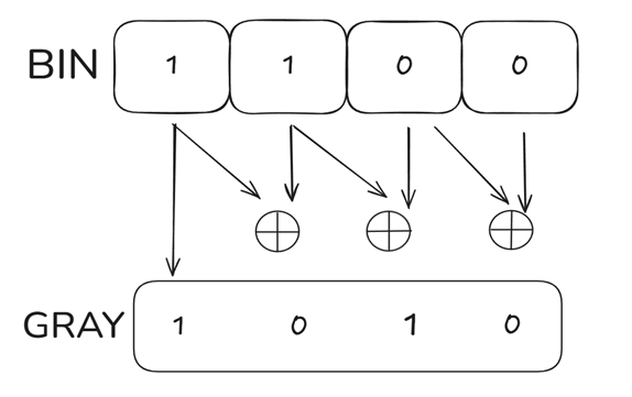
Figure 1: Binary to gray code conversion schematic
Conversion from Gray code to binary: from left to right, retain the highest bit of the Gray code as the highest bit of the binary, the next highest bit of the binary is the highest bit of the binary code and the next highest bit of the Gray code for the value of XOR operations and so forth, as illustrated in Figure 2:
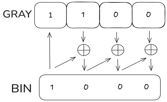
Figure 2: Gray code to binary conversion schematic
It should be noted that the use of this method must satisfy two conditions, the first is that the design is only used in the case of sequential increase in address or value, and the second point is that the design must be synchronized from a slow clock to a fast clock, otherwise there will be a data sampling omission.
2.2. Empty and Full Flag Bit, Void Full, Void Empty, and Asynchronous FIFO verilog code implementation
When determining write full and read empty, the designer usually adds an empty full judgment flag bit to the highest bit. A common practice is to add a bit to the leftmost of the pointer data as an identification bit. For example, a depth of 8 ram, when the FIFO is full, write pointer changes to 1000 from 0111 and Gray code is 1100, however, read pointer Gray code is 0000. Regardless of the bit width of the pointer, write pointer and read pointer Gray code of the upper two values of the opposite and the last two of the same case is write full, write pointer read pointer Gray code is exactly the same situation is to read the case of empty. Since there is a delay in synchronization across the clock domain, there is a false full and a false null, when the read pointer is already pointing to the next bit and has started to read the data, because of the delay, the write portion of the signal is still not received, so the state is still a full signal.
Hongke Li et al. according to the principle of the implementation of asynchronous FIFO design of the verilog code, the main module for the following aspects; FIFO memory settings, write counter to read clock domain synchronization, read counter to write clock domain synchronization, Gray code counter module, in addition to the two-stage synchronizer settings as well as the asynchronous FIFO external interfaces, the external interfaces are defined in Table 1[5]:
Table 1: External interface definition for Asynchronous FIFO[5]
Pin | Input/Output | Function |
rst_n | Input | Global reset signal, active-low |
wclk | Input | Write Clock |
rclk | Input | Read Clock |
data_in[n-1:0] | Input | Write n-bit bit-width data |
Data_out[n-1:0] | Output | Read n-bit wide data |
Write_en | Input | Write enable signal, active high |
Read_en | Input | Read enable signal, active high |
full | Output | Full standard bit, active-high |
empty | Output | Empty standard bit, active -low |
Hongke Li et al. used two methods for simulation verification, one method is to write full and then read empty directly at one time, the second method is to write full and then read out the data in two times and read empty in two steps, and the simulation results are fully compliant with the design of asynchronous FIFO.
2.3. A flexible FIFO-depth design
FIFO read/write operation changes, each gray code changes only one, taking into account the binary code cycle to clear the zero, the depth of the FIFO must be 2 times the factorial, Bo Zhang designed a more flexible structure, this structure can be set to any depth of the FIFO, closer to the actual application scenarios. Bo Zhang will gray code cycle reset rules and binary code cycle reset rules are designed separately, when the binary code due to the address cycle to clear 0, Gray code can not follow the please 0, the design method in this paper, Gray code is designed to always not clear 0, the use of Gray code data of the maximum bit width of the automatic clearing of 0[6].
After synchronization, the gray code of the read address is converted back to binary, and then the gray code of the write address is converted back to binary, and the two are subtracted to get the number of occupied as well as the number of free storage devices. The full state judgment flowchart is shown in Figure 3, and an example of asynchronous FIFO random depth implementation is shown in Table 2:
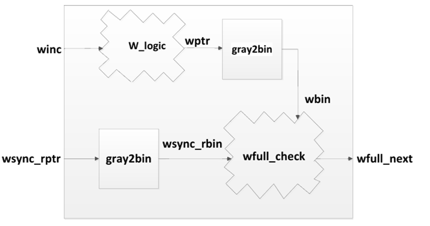
Figure 3: Flowchart for determining the full state[6]
Table 2: Examples of random depth implementations[6]
circle\signals | w_addr | wptr | wsync_rptr | wsync_fill_count |
1 | 0000 | 0000 | 0000 | 0 |
2 | 0001 | 0001 | 0001 | 0 |
3 | 0011 | 0010 | 0001 | 1 |
… | … | … | … | … |
13 | 1100 | 1010 | 0001 | 11 |
14 | 0000 | 1011 | 0001 | 12 |
15 | 0001 | 1001 | 0001 | 13 |
2.4. Optimization of UART communication protocol based on Asynchronous FIFO
FIFO chips are a new form of large-scale integrated circuit and being utilized increasingly in high-speed data collection, highspeed data processing, high-speed data transmission, and multi-machine processing systems[7]. Communication protocols are used to communicate between computers, giving computers as well as network connections a standard that must be adhered to for communication, UART (Universal Asynchronous Receiver/Transmitte) is a walk-through, asynchronous communication protocol. Time-varying systems applied to UART communication networks may cause system instability, resulting in timing chaos, data loss, transmission errors, etc. Therefore, W. Wang used Asynchronous FIFO to design the buffers.,When the amount of write data suddenly increased, but the read data rate is more uniform, you can use asynchronous FIFO to ensure that the data will not be lost, the main design of the asynchronous FIFO in the following modules,as shown in the Table 3[8].
Table 3: Examples of random depth implementations [6]
FIFO_buffer | First-in, first-out (FIFO) buffer that can be accessed by both the write clock domain and the read clock domain at the same time[8] |
sync_read/write | Make that the write clock field and the read pointer match[8]. |
sync_write/read | Ensure that the write pointer is same to the read clock domain[8]. |
Read pointer_empty | The module has the FIFO read pointer and null flag and is completely synchronized with the read clock domain[8]. |
Write pointer_full | The FIFO write pointer and full flag are included in this completely synchronized module with the write clock domain[8]. |
The results show that after utilizing the asynchronous FIFO, there is enough buffer time after writing data into the buffer. At the same time, the receiving area is also receiving at a stable rate and the buffer make data transmit to each other one by one. The buffer meets the design requirements.
The optimal gain matrix of the control system is obtained by calculating the equation solution through matlab code[8]. In Ncs, delay is unavoidable, however, the large delay of the signal in the system can be avoided. The designer models the control system of the communication network, using the pre-buffer to control the delay time. On this basis, Wenyu Wang find the answer of optimal number of samples and the upper limit of each data bit .Then, with the intention of enhancing the transmission accuracy and reduce BER, Wenyu Wang used a sampling frequency of 3 times the frequency[8].
The findings suggest that the designed asynchronous circuit outstrips the conventional method in terms of immunity to interference, the efficiency of transmission, and bit error rate[8],However, the design of setting the data buffer through asynchronous FIFO increases the energy consumption of the circuit as well as the resource consumption during hardware design, which is to be further optimized subsequently.
2.5. Asynchronous FIFO buffer design for Noc
Targeting processor elements with NoC technology allows for on-chip communication by rerouting data from the source. In order to reduce data loss in the case of multiple data streams, most NoC architectures still have buffers configured at the input or output ports, albeit at a higher cost. [9]. Suruchi Chaturvedi designed two different asynchronous circular FIFO buffers, an asynchronous design and a synchronous design, the synchronized design is illustrated in Figure 4:
Figure 4: Synchronous FIFO buffer architecture[9].
To latch the data, a completion detector (CD) is used. The CD is a static CMOS two-input NOR gate. These CD outputs operate the write and read controllers [9]. Asynchronous FIFO buffer is illustrated in Figure 5:
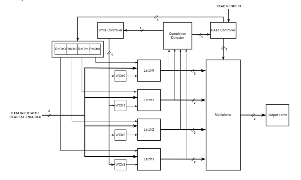
Figure 5: Asynchronous FIFO buffer architecture[9]
Simulations showed that the average power loss of the four-stage synchronous FIFO buffer is 28.57pW, while the asynchronous counterpart is only 14.93pW[9]. the latter's power consumption is reduced by almost 50 percent[9].
Asynchronous buffer designs exhibit excellent write latency performance compared to synchronous buffers. Asynchronous buffer designs perform very well in reducing write latency compared to synchronous buffers. The improved latency using buffers reduces the read time and greatly improves the read efficiency, thus allowing for improved average cycle time and throughput [9]. In addition, in this design, the designer has reduced the number of transistors used which reduces power consumption and reduces the area of the chip.
2.6. Handshake-based synchronization for multi-bit data transfer across clock domains
The handshake synchronization is based on two modules A and B. A and B are the sender and receiver respectively, the two modules use different clocks, in the A clock, the request signal is elevated and the signal is synchronized to the b clock after tapping and the signal is sampled in the b clock domain. The received signal is elevated and synchronized to the clock domain and when the transmitter module receives the acknowledgment signal, it sends the data to the receiver. The design reduces the data transmission errors, as the next set of data can only be sent by the transmitter after the request signal and the acknowledgment signal have occurred, which greatly reduces the possibility of errors occurring during the data transmission process. The structure of the handshake synchronization module is shown in Figure 6:
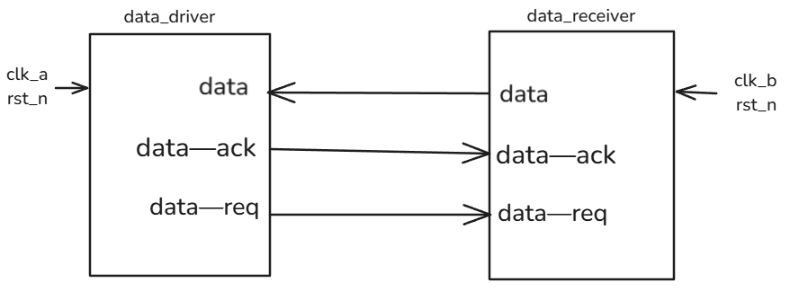
Figure 6: Handshake synchronization diagram
2.7. Asynchronous FIFO (clockless) design using handshake signals
In an attempt to enhance the performance of a design, designers are adding more and more processing elements (PEs) that can communicate with each other on the system-on-chip (SOC). In a traditional design, different processing elements have different clock sources, which may not satisfy the clock build-up and hold times during cross-clock transfer and generate substabilities that lead to data loss. S. Chaturvedi, S. M. N proposed a new architecture for the processing elements, where each of them has an asynchronous FIFO. The circuit does not rely on the clock signals, but instead uses a request ( Request) and Acknowledge) signals for operation control. This design reduces the dependence on the clock system, improves system reliability and immunity to interference, and is suitable for low-power applications such as Internet of Things (IoT) communication solutions[10]. Figure 7 shows the timings for asynchronous write operations and read operations.
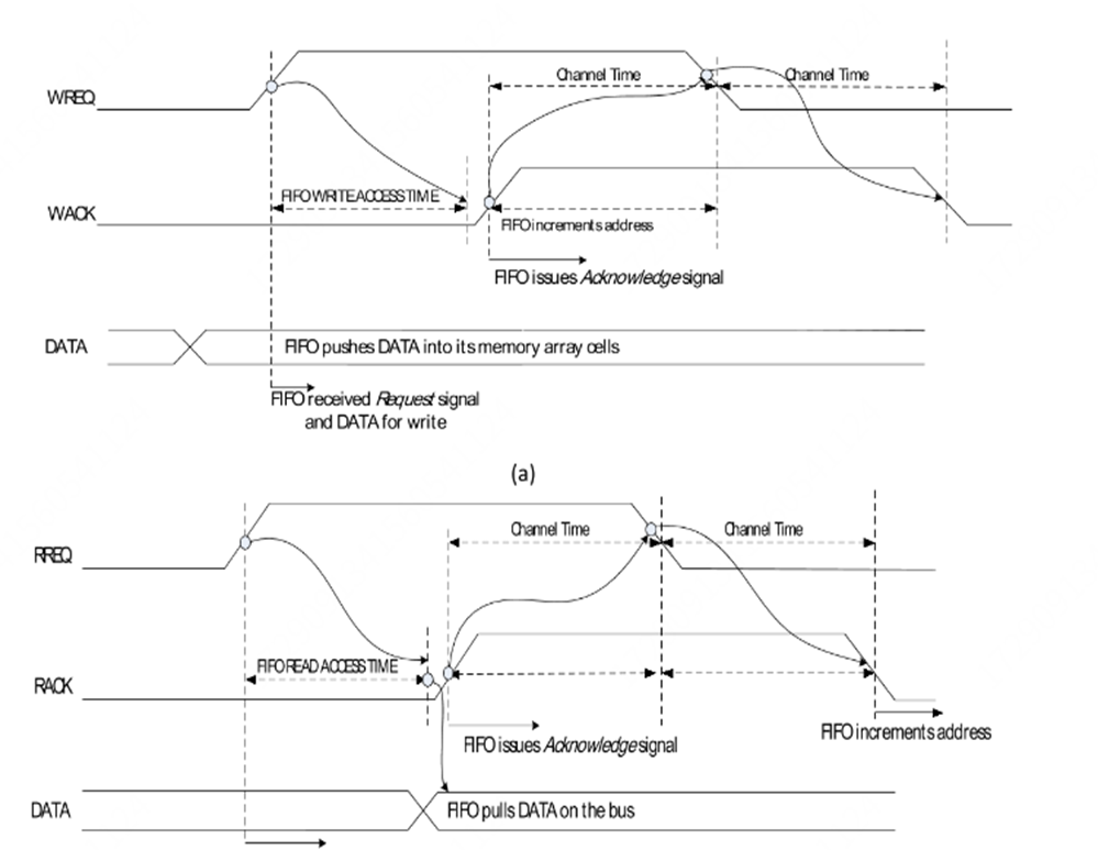
Figure 7: (a)Asynchronous write operation; (b) Asynchronous read operation[10]
Figure 8 shows the asynchronous signaling circuit:
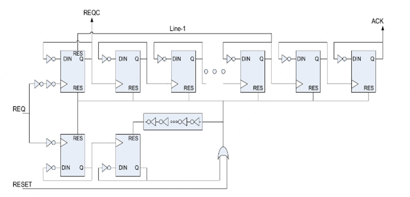
Figure 8: Asynchronous signaling circuit[10]
The simulation results show that the read operation can appear to be executed on the bus after a delay of 20 gates, which is about 0.02 seconds per gate. For the read request signal, it can appear on the bus after 0.5 nanoseconds. For the write request signal, the edge relative to the write request signal is written after a delay of 12 gates, which is about 0.25 nanoseconds [10]
3. Conclusion
Asynchronous FIFO, as a modern integrated circuit technology, shows full advantages in solving data transfer between different clock domains, buffer design, etc. This paper provides a comprehensive review of various asynchronous FIFO designs. Asynchronous FIFO is a useful design for finding the solution to data transfer across clock domains. Nowadays, in terms of electronic system design , whether it is a buffer, memory controller, or data acquisition system, asynchronous FIFO can be used to achieve a higher level of stability of the data transfer and achieve better system performance. The future design can be centered around reducing design power consumption and utilizing semiconductor processes to improve integration.
References
[1]. Patel, V., Mer, V., Patoliya, J., & Soni, B. (2023). Design & implementation of novel asynchronous FIFO. In 2023 IEEE International Symposium on Smart Electronic Systems (iSES) (pp. 292-295).
[2]. Xie, E., & Zhou, J. (2023). Analysis and comparison of asynchronous FIFO and synchronous FIFO. In 2023 IEEE 2nd International Conference on Electrical Engineering, Big Data and Algorithms (EEBDA) (pp. 260-264).
[3]. Zhang, Y., Yi, C., Wang, J., & Zhang, J. (2011). Asynchronous FIFO implementation using FPGA. International Conference on Electronics and Optoelectronics (pp. V3-207-V3-209). Himanshu, & Charan, C. (2024). A 16-byte asynchronous gray code FIFO memory using Verilog HDL for real-time applications. In 2024 2nd International Conference on Device Intelligence, Computing and Communication Technologies (DICCT).
[4]. Li, H., Wang, Q., & Yu, S. (2021). Asynchronous FIFO design based on Verilog HDL. *Electronic Design Engineering, 29(19), 107111+116.
[5]. Zhang, B. (2015). Design and formal verification of SOC-based asynchronous FIFO. Xi'an Electronic Science and Technology University.
[6]. Hao, Z., Liu, L., & Tian, B. (2023). The principle and applications of asynchronous FIFO. In 2023 IEEE 2nd International Conference on Electrical Engineering, Big Data and Algorithms (EEBDA) (pp. 277-279).
[7]. Wang, W. (2023). Optimization of UART communication protocol based on frequency multiplier sampling technology and asynchronous FIFO. In 2023 IEEE 2nd International Conference on Electrical Engineering, Big Data and Algorithms (EEBDA) (pp. 280-285).
[8]. Chaturvedi, S., M, S. N., & Rao, R. (2022). Design of asynchronous circular FIFO buffer for asynchronous network on chips. In 2022 International Conference on Distributed Computing, VLSI, Electrical Circuits and Robotics (DISCOVER) (pp. 66-71).
[9]. Abdel-Hafeez, S., & Quwaider, M. Q. (2020). A one-cycle asynchronous FIFO queue buffer circuit. International Conference on Information and Communication Systems (ICICS) (pp. 388-393).
Cite this article
Wang,Q. (2025). A Study of Advances in Asynchronous FIFO Design. Applied and Computational Engineering,121,14-23.
Data availability
The datasets used and/or analyzed during the current study will be available from the authors upon reasonable request.
Disclaimer/Publisher's Note
The statements, opinions and data contained in all publications are solely those of the individual author(s) and contributor(s) and not of EWA Publishing and/or the editor(s). EWA Publishing and/or the editor(s) disclaim responsibility for any injury to people or property resulting from any ideas, methods, instructions or products referred to in the content.
About volume
Volume title: Proceedings of the 5th International Conference on Signal Processing and Machine Learning
© 2024 by the author(s). Licensee EWA Publishing, Oxford, UK. This article is an open access article distributed under the terms and
conditions of the Creative Commons Attribution (CC BY) license. Authors who
publish this series agree to the following terms:
1. Authors retain copyright and grant the series right of first publication with the work simultaneously licensed under a Creative Commons
Attribution License that allows others to share the work with an acknowledgment of the work's authorship and initial publication in this
series.
2. Authors are able to enter into separate, additional contractual arrangements for the non-exclusive distribution of the series's published
version of the work (e.g., post it to an institutional repository or publish it in a book), with an acknowledgment of its initial
publication in this series.
3. Authors are permitted and encouraged to post their work online (e.g., in institutional repositories or on their website) prior to and
during the submission process, as it can lead to productive exchanges, as well as earlier and greater citation of published work (See
Open access policy for details).
References
[1]. Patel, V., Mer, V., Patoliya, J., & Soni, B. (2023). Design & implementation of novel asynchronous FIFO. In 2023 IEEE International Symposium on Smart Electronic Systems (iSES) (pp. 292-295).
[2]. Xie, E., & Zhou, J. (2023). Analysis and comparison of asynchronous FIFO and synchronous FIFO. In 2023 IEEE 2nd International Conference on Electrical Engineering, Big Data and Algorithms (EEBDA) (pp. 260-264).
[3]. Zhang, Y., Yi, C., Wang, J., & Zhang, J. (2011). Asynchronous FIFO implementation using FPGA. International Conference on Electronics and Optoelectronics (pp. V3-207-V3-209). Himanshu, & Charan, C. (2024). A 16-byte asynchronous gray code FIFO memory using Verilog HDL for real-time applications. In 2024 2nd International Conference on Device Intelligence, Computing and Communication Technologies (DICCT).
[4]. Li, H., Wang, Q., & Yu, S. (2021). Asynchronous FIFO design based on Verilog HDL. *Electronic Design Engineering, 29(19), 107111+116.
[5]. Zhang, B. (2015). Design and formal verification of SOC-based asynchronous FIFO. Xi'an Electronic Science and Technology University.
[6]. Hao, Z., Liu, L., & Tian, B. (2023). The principle and applications of asynchronous FIFO. In 2023 IEEE 2nd International Conference on Electrical Engineering, Big Data and Algorithms (EEBDA) (pp. 277-279).
[7]. Wang, W. (2023). Optimization of UART communication protocol based on frequency multiplier sampling technology and asynchronous FIFO. In 2023 IEEE 2nd International Conference on Electrical Engineering, Big Data and Algorithms (EEBDA) (pp. 280-285).
[8]. Chaturvedi, S., M, S. N., & Rao, R. (2022). Design of asynchronous circular FIFO buffer for asynchronous network on chips. In 2022 International Conference on Distributed Computing, VLSI, Electrical Circuits and Robotics (DISCOVER) (pp. 66-71).
[9]. Abdel-Hafeez, S., & Quwaider, M. Q. (2020). A one-cycle asynchronous FIFO queue buffer circuit. International Conference on Information and Communication Systems (ICICS) (pp. 388-393).