


1. Introduction
In all conductors, due to the continuous fluctuation of internal charges, there will be random fluctuations in voltage. These charges are in a state of thermal excitation, and from a thermodynamic perspective, the thermal motion of the atoms inside the conductor is in equilibrium. This irregular motion of charges exhibits different voltage change characteristics in different conductors. Although such fluctuations may be theoretically inevitable, they are generally undesirable in practical applications. Typically, this unwelcome voltage fluctuation is referred to as noise. For most circuits, operational amplifiers play a crucial role in signal processing, but internal noise sources limit their performance. Johnson's research proved the impact of noise on electronic engineering as early as 1928; therefore, the limit of sensitivity of an electronic circuit must be set at the critical point where the signal-to-noise ratio is just about to drop to an acceptable limit.
This paper aims to delve into the optimization of noise performance in operational amplifiers, proposing a series of effective noise reduction methods through theoretical introduction and experimental evidence. The article first provides a detailed analysis of common noise types in operational amplifiers, discussing the mechanisms and characteristics of these noises. Based on the noise theory foundation, this paper proposes three noise reduction methods: circuit design optimization, shielding processes, and physical layer design. In the circuit design optimization section, measures such as selecting appropriate components and adjusting circuit layouts effectively reduce noise. The shielding processes section explores the application of electrostatic, electromagnetic, and magnetic shielding technologies in reducing external interference. The physical layer design section, from the perspective of component size selection, analyzes how to reduce noise by changing the gate length-to-width ratio of MOS transistors or the size of the input resistance.
This paper is divided into five chapters, systematically studying the optimization of noise performance in operational amplifiers. The first chapter is the introduction, which first introduces the research background and significance of the paper, elaborating on the impact of noise on the performance of operational amplifiers and the importance of noise reduction research. The second chapter is the noise theory foundation, which provides a detailed analysis of common noise types in operational amplifiers and their generation mechanisms. The third chapter is the noise performance optimization methods, introducing three noise reduction methods: circuit design optimization, shielding processes, and physical layer design, and analyzing the effectiveness of these methods in practical applications. Finally, the conclusion summarizes the entire paper, pointing out the innovative points and practical application value of the research, and provides an outlook on future research directions.
2. Types and Formulas of Noise
Generally, noise is now commonly classified into five types: Thermal Noise, Shot Noise, Flicker Noise, Avalanche Noise, and Burst Noise. In the design of operational amplifier circuits, it is often considered that Burst Noise and Avalanche Noise have little impact on performance. Even if they do exist, they can be eliminated through appropriate measures. Therefore, when conducting noise analysis, these two types of noise do not need to be taken into account. Next, this paper will explore different sources of noise in detail [1].
2.1. Thermal Noise
Thermal noise, also known as Johnson noise, is generated by the irregular thermal motion of charge carriers (such as electrons or holes) inside a conductor. This noise phenomenon is universally present in all passive resistive materials. As a type of white noise, thermal noise is independent of the flow of current and is directly proportional to the absolute temperature of the material. Thermal noise can be represented in the form of voltage or current [2]. In a resistor, the main source of noise is thermal noise, which is equivalent to adding a voltage source in series with an ideal noise-free resistor or paralleling a current source as its noise model, as shown in Figure 1 [3].
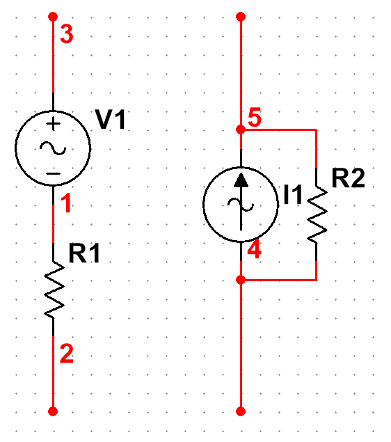
Figure 1: noise model
The equivalent noise current and voltage are given by the formulas:
\( i_{n}^{2}=\int \frac{4kT}{R}df\ \ \ \) (1)
\( {e^{2}}=\int 4kTRdf\ \ \ \) (2)
where k is the Boltzmann constant (1.38*10^(-23)J/K), T is the absolute temperature, and R is the resistance of the conductor (in ohms).
2.2. Shot Noise
Shot noise is closely related to the flow of current, which occurs when charge carriers cross a potential barrier and the conductor is not in thermal equilibrium. Due to the random nature of charge carrier crossings, a series of random and independent current pulses are generated. Shot noise is defined by the formula:
\( i_{n}^{2}={(i-{i_{D}})^{2}}=\int 2q{i_{D}}df\ \ \ \) (3)
Shot noise is not affected by temperature and maintains a constant spectral density over a specific frequency range, making it a type of white noise with a flat frequency spectrum and uniformly distributed power density [4].
2.3. Flicker Noise
Under low-frequency conditions, the noise spectral density increases by 3 dB per octave, known as "1/f noise," which is also the alias for flicker noise. Flicker noise is associated with direct current and has many different causes. The calculation formula for flicker noise is:
\( \bar{{e^{2}}}=\int (\frac{k_{e}^{2}}{f})df\ \ \ \) (4)
where \( {k_{e}} \) is an appropriate device constant for voltage [1].
3. Noise Reduction Methods
3.1. Circuit Design Optimization
Optimizing the circuit design by choosing the right components and tweaking the layout can really help in keeping the noise down. For instance, using a cascode input structure with a common source and common gate can significantly lower input noise [5]. Additionally, in the noise control design of operational amplifiers, the performance of the input stage is crucial, as its noise level directly affects the noise performance of the entire operational amplifier. When designing operational amplifiers, the primary consideration for the first stage is often not gain but noise control. Since the noise factor of PMOS transistors is relatively low, this helps to reduce input noise voltage. Therefore, the input stage typically employs a differential input structure built with PMOS transistors. Figure 2 shows a common long-tailed differential circuit [6-8].
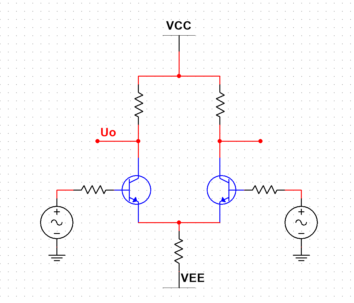
Figure 2: a common long-tailed differential circuit
3.2. Shielding Techniques
When crafting operational amplifiers with low noise, it's worth looking into shielding techniques [9]. They can make a big difference by cutting down on the noise that outside interference brings into the system. To achieve this goal, three types of shielding methods are commonly employed: electrostatic shielding, electromagnetic shielding, and magnetic shielding.
For instance, when crafting the pre-amplifier of an oscilloscope, Tang Qilun utilized double-layer electromagnetic shielding technology. Initially, he employed a copper plate of a certain thickness as the casing; the high conductivity and excellent grounding capabilities of copper provided electrostatic and electromagnetic shielding. Subsequently, within the copper casing, he filled it with black, non-conductive heat-dissipating material and added a layer of molybdenum alloy shielding, which also required proper grounding. The high magnetic conductivity of the molybdenum alloy effectively isolated external low-frequency magnetic fields. Should higher quality magnetic shielding be necessary, an additional concentric molybdenum alloy box with slightly smaller outer dimensions could be added.
Moreover, the method of coherent signal excitation shielding can be employed to create low-noise preamplifiers. This technique involves obtaining an excitation signal from the emitter or source of the amplifier's first stage that is identical in magnitude and phase to the signal, and adding it to the input jack. This envelops the weak input signal, thereby significantly reducing interference. Additionally, the first stage of the preamplifier and key components should be specifically isolated and shielded to prevent the influence of subsequent stages on the preceding ones [10].
3.3. Physical Layer Design
Beyond the circuit level, noise optimization can also be approached from the perspective of physical layer design. Selecting appropriately sized circuit components can effectively reduce the impact of noise on operational amplifiers, such as choosing the right gate length-to-width ratio of MOS transistors or incorporating resistors of suitable size. In the research of Wang Xin'an and Huang Linghua, they used Winbond's 0.5-micron CMOS standard process to analyze the noise performance of operational amplifiers. [6] By observing the impact of input and load transistors on noise, they concluded that as the size of the input transistors and load transistors increased, the noise characteristics improved. However, due to limitations in layout design and circuit stability, an excessively large L value cannot be chosen. Through the same simulation analysis, they found that the width-to-length ratio of the input transistors also affects noise characteristics. Therefore, noise can be improved by altering the resistance and the width-to-length ratios of the input and load transistors. Table 1 lists the basic simulation results, showing that the operational amplifier employed a low static current design, thereby achieving low noise characteristics, high power supply rejection ratio, and fast switching speed [6].
Table 1: Performance Parameters of the Operational Amplifier
Supply Voltage | 5V |
Quiescent Current | 400μA |
Equivalent Input Noise | 134nV/ \( \sqrt[]{Hz} \) |
Phase Threshold | 67 |
Gain Threshold | 11.5dB |
Low Frequency Gain | 85dB |
Common Mode Rejection Ratio | 85dB |
Power Supply Rejection Ratio | 75dB |
Conversion Rate | 30V/μs |
20Hz-20KHz Input Noise | 18μV |
4. Conclusion
This paper has conducted an in-depth study of the noise performance of operational amplifiers, systematically analyzing the mechanisms behind noise generation and proposing effective noise reduction methods. The article begins by categorizing and analyzing the types of noise found in operational amplifiers, revealing their behavior and impact under different conditions. Based on the analysis of noise causes, the paper cites three noise reduction strategies: circuit design optimization, shielding techniques, and physical layer design. The research results indicate that these three noise reduction strategies significantly enhance the noise performance of operational amplifiers, providing strong support for improving the overall performance of electronic systems. Although this paper has achieved certain results in noise reduction, with the advancement of technology, there will be more challenges in the future. For instance, as the dimensions of integrated circuits continue to shrink, how to achieve lower noise at smaller scales and how to more effectively combine various noise reduction technologies are issues worth further exploration.
References
[1]. He Zhengrong. (2006). Noise analysis and design of operational amplifier circuits. Microelectronics, 148-153.
[2]. Hyungseup K, Kwonsang H, Jaesung K, et al. (2020). Chopper-Stabilized Low-Noise Multipath Operational Amplifier with Dual Ripple Rejection Loops. IEEE Transactions on Circuits and Systems II: Express Briefs, 67(11), 1-1.
[3]. Wi J, Choi G, Yoo M, et al. (2024). A low-noise multipath operational amplifier with Gm-shared ping-pong and ripple averaging techniques. Microelectronics Journal, 151, 106306-106306.
[4]. Zhao Junjun. (2018). Noise analysis and design of operational amplifier circuits. Electronic Testing, 62-.
[5]. Gao Xiaohua, Feng Xian. (2014). Research on filtering technology for low-noise multi-stage amplification signal conditioning. Mini-Machines & Applications, 76-78+81. doi:10.19358/j.issn.1674-7720.2014.03.024.
[6]. Huang Linhua, Wang Xinan, & Liu Wei. (2008). Noise analysis and design of operational pre-amplifiers. China Integrated Circuit, 56-60.
[7]. Li P, Luo L, & Wei Q. (2024). A low noise CLASS AB operational amplifier with high voltage output capability by 180 nm BCD process. Journal of Physics: Conference Series, 2807(1), 012009-012009.
[8]. Apinunt T. (2022). Design procedure for noise and power optimisation of CMOS folded-cascode operational transconductance amplifier based on the inversion coefficient. Analog Integrated Circuits and Signal Processing, 111(2), 201-214.
[9]. Ruikai Z, & Chenjian W. (2023). A 4.21-μV Offset Voltage and 42-nV/√Hz Input Noise Chopper Operational Amplifier with Dynamic Element Matching. Journal of Circuits, Systems and Computers, 32(17).
[10]. Tang Qilong. (1984). Several process methods for reducing amplifier noise. Electronic Technology, 47-48+28+31.
Cite this article
Tsai,J. (2025). Research and Design on Noise Performance Optimization of Operational Amplifiers. Applied and Computational Engineering,122,29-34.
Data availability
The datasets used and/or analyzed during the current study will be available from the authors upon reasonable request.
Disclaimer/Publisher's Note
The statements, opinions and data contained in all publications are solely those of the individual author(s) and contributor(s) and not of EWA Publishing and/or the editor(s). EWA Publishing and/or the editor(s) disclaim responsibility for any injury to people or property resulting from any ideas, methods, instructions or products referred to in the content.
About volume
Volume title: Proceedings of the 5th International Conference on Materials Chemistry and Environmental Engineering
© 2024 by the author(s). Licensee EWA Publishing, Oxford, UK. This article is an open access article distributed under the terms and
conditions of the Creative Commons Attribution (CC BY) license. Authors who
publish this series agree to the following terms:
1. Authors retain copyright and grant the series right of first publication with the work simultaneously licensed under a Creative Commons
Attribution License that allows others to share the work with an acknowledgment of the work's authorship and initial publication in this
series.
2. Authors are able to enter into separate, additional contractual arrangements for the non-exclusive distribution of the series's published
version of the work (e.g., post it to an institutional repository or publish it in a book), with an acknowledgment of its initial
publication in this series.
3. Authors are permitted and encouraged to post their work online (e.g., in institutional repositories or on their website) prior to and
during the submission process, as it can lead to productive exchanges, as well as earlier and greater citation of published work (See
Open access policy for details).
References
[1]. He Zhengrong. (2006). Noise analysis and design of operational amplifier circuits. Microelectronics, 148-153.
[2]. Hyungseup K, Kwonsang H, Jaesung K, et al. (2020). Chopper-Stabilized Low-Noise Multipath Operational Amplifier with Dual Ripple Rejection Loops. IEEE Transactions on Circuits and Systems II: Express Briefs, 67(11), 1-1.
[3]. Wi J, Choi G, Yoo M, et al. (2024). A low-noise multipath operational amplifier with Gm-shared ping-pong and ripple averaging techniques. Microelectronics Journal, 151, 106306-106306.
[4]. Zhao Junjun. (2018). Noise analysis and design of operational amplifier circuits. Electronic Testing, 62-.
[5]. Gao Xiaohua, Feng Xian. (2014). Research on filtering technology for low-noise multi-stage amplification signal conditioning. Mini-Machines & Applications, 76-78+81. doi:10.19358/j.issn.1674-7720.2014.03.024.
[6]. Huang Linhua, Wang Xinan, & Liu Wei. (2008). Noise analysis and design of operational pre-amplifiers. China Integrated Circuit, 56-60.
[7]. Li P, Luo L, & Wei Q. (2024). A low noise CLASS AB operational amplifier with high voltage output capability by 180 nm BCD process. Journal of Physics: Conference Series, 2807(1), 012009-012009.
[8]. Apinunt T. (2022). Design procedure for noise and power optimisation of CMOS folded-cascode operational transconductance amplifier based on the inversion coefficient. Analog Integrated Circuits and Signal Processing, 111(2), 201-214.
[9]. Ruikai Z, & Chenjian W. (2023). A 4.21-μV Offset Voltage and 42-nV/√Hz Input Noise Chopper Operational Amplifier with Dynamic Element Matching. Journal of Circuits, Systems and Computers, 32(17).
[10]. Tang Qilong. (1984). Several process methods for reducing amplifier noise. Electronic Technology, 47-48+28+31.