


1. Introduction
Perovskites refer to compounds with the ABX3 structure type. In 2006, Kojima et al. first demonstrated the use of organic/inorganic hybrid perovskites as light-absorbing layers in solar cells at the ECS conference [1]. In 2009, Japanese scientists Miyasaka et al. introduced the organic-inorganic lead halide perovskites CH3NH3PbBr3 and CH3NH3PbI3 into dye-sensitized solar cells for the first time [2]. In 2012, Park, in collaboration with Gratzel’s research group, produced an all-solid-state solar cell with a power conversion efficiency (PCE) of 9.7%, using CH3NH3PbI3 and Spiro-OMeTAD materials [3]. In 2013, Gratzel and others achieved PSCs with an efficiency of up to 15% through a two-step sequential deposition method [4]. By 2019, the Korea Research Institute of Chemical Technology developed a new type of perovskite material via a one-step solution spin-coating method, achieving an efficiency of 24.2% and breakthroughs in stability [5]. In 2021, the Korea Research Institute of Chemical Technology, in collaboration with the Massachusetts Institute of Technology, used a chemical bath deposition method to produce high-quality SnO2 electron transport layers, raising the highest efficiency to 25.2% [6]. As of July 3, 2024, according to the globally recognized Solar Cell Efficiency Tables (Version 64), Xu Jixian’s team from the University of Chinese Academy of Sciences set a new world record with a PCE of 26.7% [7]. In just over a decade, perovskite solar cells have rapidly entered the ranks of high-efficiency solar cells, a progress made possible by improvements in material properties and continuous optimization of preparation processes.
Common A-site ions in perovskite solar cells include methylammonium (CH3NH3+ or MA+), formamidinium (NH=CHNH3+ or FA+), and cesium ions (Cs+) [8]. The B-site ions are typically lead ions, with common alternatives such as tin, germanium, bismuth, antimony, and copper. The most commonly used X-site ions are iodide ions, while pseudo-halide ions like thiocyanate (SCN-) can also partially replace iodide ions in perovskite materials. The most typical perovskite layer material in PSCs is CH3NH3PbI3, which features lead (Pb) atoms at the core of the octahedron, iodine (I) atoms at the octahedral vertices, and organic methylammonium groups at the face-centered cubic lattice corners. Perovskite materials exhibit a unique organic halide structure where halogen octahedra connect through shared vertices to form a stable three-dimensional network. This is more stable than edge- or face-sharing structures, allowing for larger ion sizes and maintaining structural stability despite crystal defects, thus facilitating defect migration [9].
Perovskite solar cells typically consist of a bottom electrode (commonly FTO or ITO conductive glass), an electron transport layer (ETL), a perovskite light-absorbing layer, a hole transport layer (HTL), and a counter electrode (either metal, such as silver or gold, or carbon-based electrodes). Based on the direction of light incidence, the cell structure can be divided into n-i-p and p-i-n types. Based on whether a mesoporous layer is present, it can be categorized as a mesoporous or planar heterojunction structure. The n-i-p structure, derived from dye-sensitized cells, is known as the conventional structure. The n-i-p mesoporous structure often employs a mesoporous TiO2 layer, which acts as a scaffold, transports electrons, and restricts perovskite crystal growth. The open-circuit voltage of the n-i-p planar heterojunction structure is higher than that of the mesoporous structure, and its preparation process is relatively simpler, though controlling the morphology of perovskite films is more challenging, leading to poor reproducibility and more pronounced hysteresis effects. The p-i-n structure, also known as the inverted structure, is mostly a planar heterojunction. Although its performance is slightly inferior to the n-i-p structure, this design avoids the high-temperature deposition of TiO2 and has weaker hysteresis effects. Structures without electron/hole transport layers take advantage of the bipolar charge transport properties of perovskites, omitting ETL or HTL and simplifying the structure. The n-i-p device without ETL avoids the high-temperature preparation of the TiO2 layer, while the structure without HTL eliminates the use of common organic hole transport materials, reducing costs and improving stability.
Compared to existing solar cell materials, perovskites offer several significant advantages, making them ideal for developing efficient, low-cost solar cells. Perovskite materials have a moderate bandgap (around 1.5 eV) [9], a high extinction coefficient, and superior light absorption capability compared to other organic dyes. Doping can be used to adjust the bandgap. Their excellent carrier transport properties allow for efficient electron and hole transport, with long carrier diffusion lengths and lifetimes. The open-circuit voltage of perovskite solar cells is much higher than that of other types of cells, and their structure is relatively simple with low manufacturing costs. The core material, hybrid perovskite, can be prepared under mild conditions through methods such as spin-coating or vapor deposition. Additionally, perovskite cells, with their ultra-light, ultra-thin, and flexible characteristics, show potential in flexible devices, tandem cells, and semi-transparent cells. However, perovskite solar cells face challenges such as poor stability and surface defects. Interface contact, ion migration, and external environmental factors (water, oxygen, light, etc.) can all lead to degradation of the functional layers and interfacial deterioration. Surface defects can act as non-radiative centers, affecting carrier diffusion, extraction, and transport within the device, thus degrading device performance. Appling interfacial engineering to address these issues can significantly improve the performance of perovskite solar cells.
2. Interface Engineering in Perovskite Solar Cells
In conventional n-i-p type perovskite solar cells, the primary interfaces include the bottom electrode/electron transport layer interface, the electron transport layer/perovskite light-absorbing layer interface, the perovskite light-absorbing layer/hole transport layer interface, and the hole transport layer/metal counter-electrode interface. In structures without a hole transport layer, there is also the perovskite light-absorbing layer/electrode interface, and in structures without an electron transport layer, there is the bottom electrode/perovskite light-absorbing layer interface. The properties of these interfaces, especially those related to the perovskite light-absorbing layer, are critical for both device efficiency and stability. Therefore, interface engineering aimed at addressing various issues, such as defect passivation, suppression of non-radiative recombination, prevention of perovskite degradation, and improvement of carrier transport dynamics, can significantly enhance the efficiency and long-term stability of perovskite solar cells.
2.1. Optimizing interface energy level alignment
The energy level differences at interfaces determine the efficiency of carrier extraction and transport. Efficient carrier extraction and transport can only be achieved when the energy level differences between adjacent materials are well-matched, thereby improving the photocurrent. In perovskite solar cells, a contact barrier (ФFC) of about 0.70 eV is formed between the ITO substrate (work function ~4.77 eV) and the SnO₂ electron transport layer (work function ~4.05 eV). Figure 1 a) shows the impact of ФFC on the performance of PSCs simulated via drift-diffusion. The results indicate that larger ФFC values lead to higher energy loss at the front contact, thus reducing efficiency. To address this issue, Yang et al. [10] applied interface engineering by introducing an atomic layer deposition (ALD) of Al₂O₃ between ITO and the ETL. As shown in Figures 1 b) and c), the positive fixed charges in Al₂O₃ effectively reduced the work function of ITO, lowering ФFC from 0.78 eV to 0.28 eV. This significantly reduced recombination losses at the interface, ultimately increasing the PCE to 25.7%.
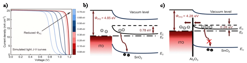
Figure 1: a) Simulated J-V curves under different ФFC values. Schematic illustration of energy band diagrams at front contact.b) without Al2O3.c) with Al2O3 [10].
2.2. Improving carrier transport dynamics
In perovskite photovoltaic devices, TiO₂ is often used as the electron transport layer (ETL), but its low electron mobility limits performance enhancement. Researchers have designed various TiO₂ nanostructures, such as nanorods, nanowires, nanotubes, and layered nanostructures, to further improve TiO₂’s photoelectric properties. Fang Guojia et al. [11] employed a hydrothermal treatment method using NaOH to create a TiO₂ nanowire framework for the ETL, enhancing carrier transport performance. Additionally, doping the TiO₂ electron transport layer is another method to improve carrier transport performance. For example, doping with small amounts of YAc₃, ZnAc₂, and ZrAc₄ (at ratios of 0.05% to 0.1%) significantly improved electron mobility, achieving device efficiencies above 15% [12].
2.3. Defect passivation
Defects can induce non-radiative recombination of carriers, which negatively impacts the PCE (as shown in Figure 2 a). These defects also accelerate the permeation of water and oxygen into the perovskite film, resulting in perovskite degradation and reduced cell lifespan.. Since the defect density at the interface (top and bottom of the film) is much higher than in the bulk [13], interface engineering to passivate these defects is crucial for improving cell performance. Kim et al. [14] used a mixture of N,N-dimethylformamide (DMF) and γ-butyrolactone (GBL) solvents to dissolve the CH₃NH₃PbI₃ precursor. As shown in Figures 2 b)–d), this significantly improved the morphology of the perovskite film, reducing the probability of electron-hole recombination at the interface and thereby enhancing the performance of the perovskite photovoltaic devices.
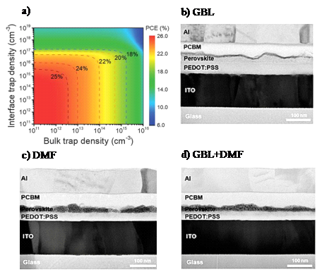
Figure 2: a) Relationship between the PCE of MAPbI₃ thin-film solar cells and the defect/trap density at the interface [13]. b)–d) Cross-sectional transmission electron microscopy (TEM) images of inverted perovskite/fullerene planar heterojunction solar cells prepared with different solvents: b) GBL, c) DMF, and d) a mixed solvent [14].
2.4. Suppressing ion migration
Ion migration-induced interface degradation is one of the key factors affecting the stability of perovskite solar cells. Voltage generated within the device drives ion migration, causing perovskite amorphization and halide segregation, which leads to the degradation of the overall device [15]. Ning et al. [16] used an “S-shaped, hook-like” organic small molecule—naphthalene diimide derivative (NDI-BN) as the cathode interface layer. The π-π stacking forces between NDI-BN molecules form a high-density stacking structure, effectively preventing ion migration and improving the stability of the device.
2.5. Enhancing stability
The intrinsic instability of lead-halide perovskite materials makes them prone to degradation under external environmental influences, altering interface properties and leading to device performance deterioration. For example, spiro-OMeTAD, a commonly used hole transport layer material, is highly hygroscopic and absorbs moisture when exposed to air. Yang et al. [17] successfully assembled a hydrophobic alkylammonium cation on the surface of the perovskite using a self-assembled monolayer (SAM) method, forming an effective water-resistant layer. Under a relative humidity of 90±5%, this layer was able to protect the perovskite film for over 30 days with almost no loss in energy conversion efficiency.
3. Additives in Interface Engineering
3.1. Organic small molecules
Organic small molecules are widely used for the modification of the interfaces between perovskite layers due to their simple structure, excellent solubility, ease of solution processing, and a wide variety of functional groups that can selectively passivate various types of defects. Hybrid halide perovskites have low formation energies, leading to uncoordinated Pb²⁺ ions on the crystal surface, which act as non-radiative recombination centers, impacting device performance. By introducing groups containing electron-donating elements (such as carbonyl, phosphate, cyano, and sulfonyl), Lewis acid-base adducts are formed with electron-deficient defects, passivating the under-coordinated lead cluster ions. Yan et al. [18] treated inverted perovskite solar cells with a diphosphine Lewis base that can passivate, bind, and bridge the interface and grain boundaries. Its power conversion efficiency stabilized at 23.5% after continuous operation over 3500 hours at about 40°C. Organic ammonium salts are another class of widely used interface modifiers, as they are dielectric materials capable of passivating both negatively and positively charged ion defects via ionic or coordination bonds. Furthermore, the dielectric properties of organic ammonium salt dipoles reduce the rate of charge recombination [19]. Fullerene and its derivatives are also commonly selected as modifiers for the ELT/perovskite interface. These are typical Lewis acid passivation molecules, with advantages such as high electron mobility, good energy level matching, wide compatibility with flexible substrates, and strong molecular structure designability [20], making them among the best electron transport layer modification materials for perovskite solar cells.
3.2. Polymer materials
In interface engineering, polymers interact with the perovskite layer in various ways, including adjusting crystallization dynamics, improving film flexibility, controlling carrier transport, and suppressing ion migration [21], thereby enhancing device performance. Additionally, the hydrophobicity and cross-linked network structure of polymers improve the stability of perovskites under complex environmental conditions and significantly reduce lead leakage, enhancing environmental safety and long-term durability. Common insulating polymers, such as polystyrene (PS), polymethyl methacrylate (PMMA), and polyethylene oxide (PEO) [22], have been reported to modify the perovskite/HTL interface, demonstrating excellent defect passivation effects and improving open-circuit voltage.
3.3. Metal oxides and halides
Metal oxides and halides can serve as passivation layers to modify the perovskite interface, as shown in Figure 3a), to optimize interface energy level alignment, promote charge transport, reduce charge recombination, and maintain the operational stability of PSCs. Metal oxides can serve as standalone charge transport layer materials and are widely used for modifying the ETL/perovskite light-absorbing layer interface. Examples include Al₂O₃, MgO, and ZrO₂ [23]. Metal halides can also form crystal clusters between the electron transport layer and the perovskite layer. As shown in Figures 3b)–c), the bright clusters in C indicate that CsBr has formed crystal clusters on the surface of c-TiO2, which can effectively suppress the precipitation of PbI₂ in the perovskite layer caused by UV light and moisture, significantly enhancing the stability of the cells. Various metal halides are applied in interface engineering, including SnCl₂, KCl, CsBr, CsCl, and others. Li et al. [24] used CsBr as an interface modifier between the electron collection layer and the CH₃NH₃PbI₃₋ₓClₓ perovskite absorber layer, as shown in Figures d)–e), increasing PCE from 11.5% to 15.3%, and the ratio of stable output power to the PCE obtained from J-V scanning increased from 0.83 to 0.90 (the value closer to 1 indicates a reduced hysteresis effect)). Under UV radiation intensity 100 times that of sunlight, after 95 minutes of irradiation, the normalized absorbance remained above 98%.
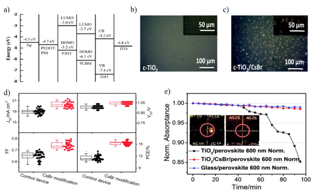
Figure 3: a) Energy level diagram of an inverted PSC device with a ZnO buffer layer [23]. b)–c) Comparison of CsBr-modified c-TiO₂ substrates. d) Performance comparison of devices modified with CsBr. e) Normalized absorption at 600 nm. The inset shows a UV aging test, where the red circle indicates the UV light window [24].
3.4. Two-Dimensional materials
In interface engineering, commonly used two-dimensional materials include graphene and its derivatives, transition metal dichalcogenides (TMDs), transition metal carbides/nitrides (MXenes), and black phosphorus (BP), among others [25]. These materials are highly valued due to their atomic-level thickness, smooth surfaces, and absence of dangling bonds. Unlike traditional interface contacts, two-dimensional materials bind to other materials through physical adsorption, forming van der Waals heterostructures, as shown in Figure 4a). This promotes the epitaxial growth of perovskite films, optimizing their crystallization and orientation while reducing defects. Additionally, 2D perovskite materials exhibit excellent hydrophobicity and stability, significantly enhancing the stability of perovskite solar cells. Zhang et al. [27] utilized the tunable bandgap and high ambipolar carrier mobility of 2D black phosphorus (BP), introducing BP nanosheets of varying thicknesses at both the ETL/perovskite interface and the perovskite/HTL interface. This enhanced the extraction of both electrons and holes, making BP a dual-functional nanomaterial, as shown in Figures 4b)–d). This not only improved carrier extraction but also reduced trap density, increasing the PCE from 16.95% to 19.83%.
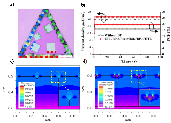
Figure 4: a) Optical image of CsPbI3/WSe2 heterostructure. The dashed lines along the edges of the monolayer WSe2 and epitaxial perovskite highlight their corresponding orientation. Scale bar: 30 μm [26]. b) Stable short-circuit current density and PCE of the devices with and without BP dual-introduction [27]. Hole current density distribution of the simulated PSCs without c) and with d) the BP modification [28].
4. Conclusion and Outlook
Perovskite solar cells have garnered significant attention due to their high photoelectric conversion efficiency and low cost. However, instability and defects at the interfaces remain major challenges. The use of interface modification techniques offers a simple and effective way to enhance performance. This paper summarizes the advantages of perovskite solar cells and introduces commonly used interface modifiers such as organic small molecules, polymers, and two-dimensional materials. Their mechanisms in optimizing energy level alignment, improving carrier dynamics, passivating defects, and suppressing ion migration are explained. The results indicate that well-designed interface engineering is crucial for improving both the efficiency and stability of devices, making it a key focus of research. In the future, the development of multifunctional, low-cost, and environmentally friendly interface modifiers, as well as modification methods suitable for large-area devices, will help accelerate the progress of perovskite solar cells.
References
[1]. Akihiro Kojima, et al. "Novel photoelectrochemical cell with mesoscopic electrodes sensitized by lead-halide compounds (11)." ECS Meeting Abstracts. No. 1. IOP Publishing, 2008.
[2]. Yaoguang Rong, et al. "Challenges for commercializing perovskite solar cells." Science 361.6408 (2018): eaat8235.
[3]. Hui-Seon Kim, et al. "Lead iodide perovskite sensitized all-solid-state submicron thin film mesoscopic solar cell with efficiency exceeding 9%." Scientific reports 2.1 (2012): 591.
[4]. Na’il Saleh, et al. "Effect of molecular-level insulation on the performance of a dye-sensitized solar cell: fluorescence studies in solid state." Journal of fluorescence 25 (2015): 59-68.
[5]. Eui Hyuk Jung, et al. "Efficient, stable and scalable perovskite solar cells using poly (3-hexylthiophene)." Nature 567.7749 (2019): 511-515.
[6]. Jason J. Yoo, et al. "Efficient perovskite solar cells via improved carrier management." Nature 590.7847 (2021): 587-593.
[7]. Martin A. Green, et al. "Solar cell efficiency tables (Version 64)." Progress in Photovoltaics: Research and Applications 32.7 (2024): 425-441.
[8]. Lixin Xiao, et al. Perovskite solar cells. Beijing:Peking University Press, 2016. 32-37.
[9]. Jing Wei, et al. "Perovskite solar cells: promise of photovoltaics." Scientia Sinica Technologica 44.8 (2014): 801-821.
[10]. Daoyong Zhang, et al. "Mitigated front contact energy barrier for efficient and stable perovskite solar cells." Energy & Environmental Science 17.11 (2024): 3848-3854.
[11]. Hong Tao, et al. "Perovskite solar cell based on network nanoporous layer consisted of TiO2 nanowires and its interface optimization." Journal of Power Sources 290 (2015): 144-152.
[12]. Hsin-Hua Wang, et al. "Improving the TiO2 electron transport layer in perovskite solar cells using acetylacetonate-based additives." Journal of Materials Chemistry A 3.17 (2015): 9108-9115.
[13]. Bo Chen, et al. "Imperfections and their passivation in halide perovskite solar cells." Chemical Society Reviews 48.14 (2019): 3842-3867.
[14]. Kim Hak-Beom, et al. "Mixed solvents for the optimization of morphology in solution-processed, inverted-type perovskite/fullerene hybrid solar cells." Nanoscale 6.12 (2014): 6679-6683.
[15]. Diego Di Girolamo , et al. "Ion migration‐induced amorphization and phase segregation as a degradation mechanism in planar perovskite solar cells." Advanced Energy Materials 10.25 (2020): 2000310.
[16]. Jiaoyi Ning, et al. "Gaining insight into the effect of organic interface layer on suppressing ion migration induced interfacial degradation in perovskite solar cells." Advanced Functional Materials 30.35 (2020): 2000837.
[17]. Shuang Yang, et al. "Functionalization of perovskite thin films with moisture-tolerant molecules." Nature Energy 1.2 (2016): 1-7.
[18]. Chongwen Li, et al. "Rational design of Lewis base molecules for stable and efficient inverted perovskite solar cells." Science 379.6633 (2023): 690-694.
[19]. Lusheng Liang, et al. "Efficient perovskite solar cells by reducing interface‐mediated recombination: a bulky amine approach." Advanced Energy Materials 10.14 (2020): 2000197.
[20]. Xiaoqin Ye, et al. "Applications of fullerene materials in perovskite solar cells." Journal of Chemical Industry and Engineering 71.06 (2020):2510-2529.
[21]. Shuo Wang, et al. "Polymers for Perovskite Solar Cells." JACS Au 4.9 (2024): 3400-3412.
[22]. Jinjing Zhou,et al ."Recent progress of interface engineering for lead halide perovskite solar cells." Library Theory and Practice 39.05 (2022):1937-1955.
[23]. Zhiqiang Liang, et al. "Effects of the morphology of a ZnO buffer layer on the photovoltaic performance of inverted polymer solar cells." Advanced Functional Materials 22.10 (2012): 2194-2201.
[24]. Wenzhe Li, et al. "Enhanced UV-light stability of planar heterojunction perovskite solar cells with caesium bromide interface modification." Energy & Environmental Science 9.2 (2016): 490-498.
[25]. Xiangqian Shen, et al. "Two-Dimensional Materials for Highly Efficient and Stable Perovskite Solar Cells." Nano-Micro Letters 16.1 (2024): 201.
[26]. Liqiang Zhang, et al. "Facet-selective growth of halide perovskite/2D semiconductor van der Waals heterostructures for improved optical gain and lasing." Nature Communications 15.1 (2024): 5484.
[27]. Meng Zhang, et al. "Synergistic cascade carrier extraction via dual interfacial positioning of ambipolar black phosphorene for high‐efficiency perovskite solar cells." Advanced materials 32.28 (2020): 2000999.
[28]. Peng You, et al. "2D materials for conducting holes from grain boundaries in perovskite solar cells." Light: Science & Applications 10.1 (2021): 68.
Cite this article
Lu,Y. (2025). Additives in Interfacial Engineering for Performance Improvement of Perovskite Solar Cells. Applied and Computational Engineering,122,92-99.
Data availability
The datasets used and/or analyzed during the current study will be available from the authors upon reasonable request.
Disclaimer/Publisher's Note
The statements, opinions and data contained in all publications are solely those of the individual author(s) and contributor(s) and not of EWA Publishing and/or the editor(s). EWA Publishing and/or the editor(s) disclaim responsibility for any injury to people or property resulting from any ideas, methods, instructions or products referred to in the content.
About volume
Volume title: Proceedings of the 5th International Conference on Materials Chemistry and Environmental Engineering
© 2024 by the author(s). Licensee EWA Publishing, Oxford, UK. This article is an open access article distributed under the terms and
conditions of the Creative Commons Attribution (CC BY) license. Authors who
publish this series agree to the following terms:
1. Authors retain copyright and grant the series right of first publication with the work simultaneously licensed under a Creative Commons
Attribution License that allows others to share the work with an acknowledgment of the work's authorship and initial publication in this
series.
2. Authors are able to enter into separate, additional contractual arrangements for the non-exclusive distribution of the series's published
version of the work (e.g., post it to an institutional repository or publish it in a book), with an acknowledgment of its initial
publication in this series.
3. Authors are permitted and encouraged to post their work online (e.g., in institutional repositories or on their website) prior to and
during the submission process, as it can lead to productive exchanges, as well as earlier and greater citation of published work (See
Open access policy for details).
References
[1]. Akihiro Kojima, et al. "Novel photoelectrochemical cell with mesoscopic electrodes sensitized by lead-halide compounds (11)." ECS Meeting Abstracts. No. 1. IOP Publishing, 2008.
[2]. Yaoguang Rong, et al. "Challenges for commercializing perovskite solar cells." Science 361.6408 (2018): eaat8235.
[3]. Hui-Seon Kim, et al. "Lead iodide perovskite sensitized all-solid-state submicron thin film mesoscopic solar cell with efficiency exceeding 9%." Scientific reports 2.1 (2012): 591.
[4]. Na’il Saleh, et al. "Effect of molecular-level insulation on the performance of a dye-sensitized solar cell: fluorescence studies in solid state." Journal of fluorescence 25 (2015): 59-68.
[5]. Eui Hyuk Jung, et al. "Efficient, stable and scalable perovskite solar cells using poly (3-hexylthiophene)." Nature 567.7749 (2019): 511-515.
[6]. Jason J. Yoo, et al. "Efficient perovskite solar cells via improved carrier management." Nature 590.7847 (2021): 587-593.
[7]. Martin A. Green, et al. "Solar cell efficiency tables (Version 64)." Progress in Photovoltaics: Research and Applications 32.7 (2024): 425-441.
[8]. Lixin Xiao, et al. Perovskite solar cells. Beijing:Peking University Press, 2016. 32-37.
[9]. Jing Wei, et al. "Perovskite solar cells: promise of photovoltaics." Scientia Sinica Technologica 44.8 (2014): 801-821.
[10]. Daoyong Zhang, et al. "Mitigated front contact energy barrier for efficient and stable perovskite solar cells." Energy & Environmental Science 17.11 (2024): 3848-3854.
[11]. Hong Tao, et al. "Perovskite solar cell based on network nanoporous layer consisted of TiO2 nanowires and its interface optimization." Journal of Power Sources 290 (2015): 144-152.
[12]. Hsin-Hua Wang, et al. "Improving the TiO2 electron transport layer in perovskite solar cells using acetylacetonate-based additives." Journal of Materials Chemistry A 3.17 (2015): 9108-9115.
[13]. Bo Chen, et al. "Imperfections and their passivation in halide perovskite solar cells." Chemical Society Reviews 48.14 (2019): 3842-3867.
[14]. Kim Hak-Beom, et al. "Mixed solvents for the optimization of morphology in solution-processed, inverted-type perovskite/fullerene hybrid solar cells." Nanoscale 6.12 (2014): 6679-6683.
[15]. Diego Di Girolamo , et al. "Ion migration‐induced amorphization and phase segregation as a degradation mechanism in planar perovskite solar cells." Advanced Energy Materials 10.25 (2020): 2000310.
[16]. Jiaoyi Ning, et al. "Gaining insight into the effect of organic interface layer on suppressing ion migration induced interfacial degradation in perovskite solar cells." Advanced Functional Materials 30.35 (2020): 2000837.
[17]. Shuang Yang, et al. "Functionalization of perovskite thin films with moisture-tolerant molecules." Nature Energy 1.2 (2016): 1-7.
[18]. Chongwen Li, et al. "Rational design of Lewis base molecules for stable and efficient inverted perovskite solar cells." Science 379.6633 (2023): 690-694.
[19]. Lusheng Liang, et al. "Efficient perovskite solar cells by reducing interface‐mediated recombination: a bulky amine approach." Advanced Energy Materials 10.14 (2020): 2000197.
[20]. Xiaoqin Ye, et al. "Applications of fullerene materials in perovskite solar cells." Journal of Chemical Industry and Engineering 71.06 (2020):2510-2529.
[21]. Shuo Wang, et al. "Polymers for Perovskite Solar Cells." JACS Au 4.9 (2024): 3400-3412.
[22]. Jinjing Zhou,et al ."Recent progress of interface engineering for lead halide perovskite solar cells." Library Theory and Practice 39.05 (2022):1937-1955.
[23]. Zhiqiang Liang, et al. "Effects of the morphology of a ZnO buffer layer on the photovoltaic performance of inverted polymer solar cells." Advanced Functional Materials 22.10 (2012): 2194-2201.
[24]. Wenzhe Li, et al. "Enhanced UV-light stability of planar heterojunction perovskite solar cells with caesium bromide interface modification." Energy & Environmental Science 9.2 (2016): 490-498.
[25]. Xiangqian Shen, et al. "Two-Dimensional Materials for Highly Efficient and Stable Perovskite Solar Cells." Nano-Micro Letters 16.1 (2024): 201.
[26]. Liqiang Zhang, et al. "Facet-selective growth of halide perovskite/2D semiconductor van der Waals heterostructures for improved optical gain and lasing." Nature Communications 15.1 (2024): 5484.
[27]. Meng Zhang, et al. "Synergistic cascade carrier extraction via dual interfacial positioning of ambipolar black phosphorene for high‐efficiency perovskite solar cells." Advanced materials 32.28 (2020): 2000999.
[28]. Peng You, et al. "2D materials for conducting holes from grain boundaries in perovskite solar cells." Light: Science & Applications 10.1 (2021): 68.