


1. Introduction
At present, the integration level of chips is increasing, while the operating speed is getting faster and the area is getting smaller, but the resulting power consumption is also increasing. The power consumption of chips can affect their performance and reliability, especially in various battery powered smart devices such as laptops, Bluetooth earphones, medical equipment, etc. Therefore, in chip design, how to reduce chip power consumption while ensuring the reliability of other chip performance has become an important issue in current integrated circuit research and development. The development of real-time clock (RTC) can be traced back to before the 21st century. Early RTC chips were essentially a frequency divider with a computer communication interface, which obtained year, month, day, hour, minute, and second time information through frequency division and counting, and then transmitted this time information to the processor through the communication interface [1]. During this period, RTC chips did not have some of the functions of a universal clock, such as not supporting automatic switching between 12/24-hour clocks, not including perpetual calendars, and not being able to automatically recognize leap years; Moreover, the chip adopts a dual in-line package and uses parallel interfaces for data transmission, which results in relatively high-power consumption and can no longer meet people's needs. The application of low-power digital real-time clocks can enhance the convenience of home life, such as automatically adjusting the running time of lights, heating, and other household appliances, bringing energy-saving effects to home life. Meanwhile, low-power digital real-time clocks also play an important role in fields such as transportation, education, and healthcare, improving the overall operational efficiency and service quality of society. It will also drive technological innovation, promote the continuous emergence of new technologies and products, and provide a continuous source of power for the progress and development of human society.
This article first introduces digital low-power technology, and after analyzing the composition of chip power consumption. Furthermore, different digital low-power technologies were discussed based on different power consumption, and a Chip system architecture was presented. Then the oscillator used was introduced, starting with the principle of oscillator, followed by a detailed introduction to the Crystal oscillator and Pierce oscillator. Finally, this article focuses on the Design of Digital Real Time Clock, which is introduced in several parts such as SPI interface module, Frequency divider, Perpetual Calendar module, etc., and then proposes the use of Power consumption optimization in front-end design.
2. Theoretical basis analysis of digital low-power technology
2.1. Composition of Power Consumption in CMOS Integrated Circuits
The power consumption of CMOS integrated circuits is mainly composed of two parts: dynamic power consumption ( \( {P_{dynamic}} \) ) and static power consumption ( \( {P_{leakage}} \) ). Dynamic power consumption is further divided into short-circuit current power consumption ( \( {P_{internal}} \) ) and dynamic switching power consumption ( \( {P_{switch}} \) ) [2]. Namely:
\( {P_{dynamic}}={P_{switch}}+{P_{internal}} \) (1)
\( {P_{total}}={P_{dynamic}}+{P_{leakage}} \) (2)
Dynamic power consumption ( \( {P_{dynamic}} \) ) refers to the power consumption of CMOS circuits during the switching process by charging and discharging the load capacitance of the output node, also known as switching power consumption. This power consumption is mainly composed of two parts:
\( {P_{switch}} \) , which stands for switching current power consumption. When a CMOS circuit switches from one state to another, such as from "0" to "1" or from "1" to "0", it generates charging and discharging currents for the load capacitance, and the power consumption generated by this current is the main part of dynamic power consumption. The main reason for dynamic switching power consumption is that the circuit needs to charge and discharge the load capacitor \( {C_{load}} \) when switching outputs, and the magnitude of this power consumption depends on: 1. the power supply voltage \( {V_{dd}} \) ; 2. Load capacitance size \( {C_{load}} \) ; 3. Frequency \( {f_{clock}} \) for charging and discharging the circuit.
\( {P_{switch}}={C_{load}}∙V_{dd}^{2}∙{f_{clock}} \) (3)
According to the above formula, it can be seen that the most effective way to reduce this part of power consumption is to lower the operating voltage of the system or submodule while ensuring the normal operation of the circuit, thus achieving the goal of saving power consumption.
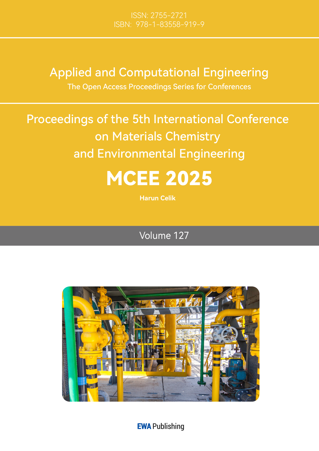
\( {P_{internal}} \) , which stands for short circuit current power consumption. Schematic diagram of short-circuit power consumption is shown in Figure 1.
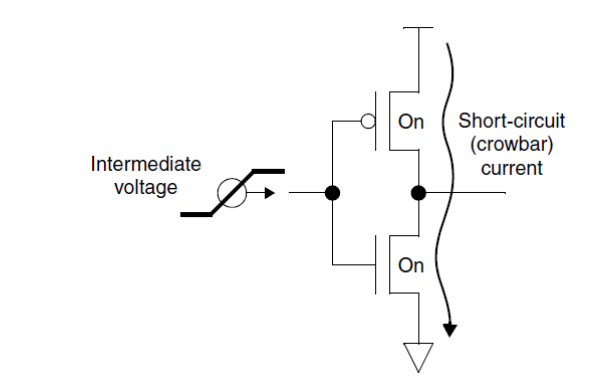
Figure 1: Schematic diagram of short-circuit power consumption
Due to the fact that the input voltage waveform is not an ideal step input signal, there are certain rise and fall times, as shown in Figure 1. When the input signal changes from 0 to 1, there will be a gradual process of change. During this process, there will be a period of time that causes the PMOS and NMOS transistors to conduct simultaneously, forming a DC conduction current from the power supply to ground, which is called short-circuit current.
The power consumption of this part is related to the power supply voltage \( {V_{dd}} \) , the duration of short-circuit current \( {t_{sc}} \) , the magnitude of short-circuit current \( {I_{peak}} \) , and the generation of clock frequency \( {f_{clock}} \) .
\( {P_{internal}}={t_{sc}}{V_{dd}}∙{I_{peak}}∙{f_{clock}} \) (4)
From the above formula, it can be seen that \( {P_{internal}} \) is directly proportional to the short-circuit current holding time \( {t_{sc}} \) and the power supply \( {V_{dd}} \) . Therefore, by optimizing the device to reduce tsc or reduce \( {V_{dd}} \) while keeping the clock frequency constant, the short-circuit power consumption of the chip can be reduced [3].
\( {P_{leakage}} \) , which stands for static power consumption. Static power consumption refers to the power consumption of CMOS circuits caused by leakage current during steady state. Although ideally there is no DC conduction current in a CMOS circuit during steady state, the static power consumption of the CMOS circuit is not zero due to leakage currents such as reverse biased PN junction current and sub threshold current of the MOS transistor. Although this part of power consumption is relatively small, it also needs to be considered in low-power design.
2.2. Research on Digital Low Power Technology
The first technique is Clock Gathering. Gate controlled clock technology reduces power consumption by controlling the switching of clock signals. When certain logic modules are not required to work, their clock signals can be temporarily cut off to avoid unnecessary power consumption. Gated clock technology is widely used in complex systems such as microprocessors and SoCs to reduce the power consumption of clock networks [3].
Another common method is Multi Threshold Voltage. This technology reduces power consumption by using transistors with different threshold voltages. Transistors with low threshold voltage can improve performance, but they will increase leakage current; Transistors with high threshold voltages can reduce leakage current, but their performance may decrease. Through rational design, a balance can be found between performance and power consumption. It is suitable for systems with strict requirements for power consumption and performance, such as SoC for mobile devices, high-performance computing servers, etc.
2.3. Chip system architecture
Chips can be divided into analog circuit design and digital function parts. The main function of the analog part is to provide working power and reference power for each module, and to provide stable clock signals to the digital part. The digital part obtains the required frequency control function output through frequency division, multiplication, etc. In the system, the bias circuit first provides reference voltage and current to each part, while the LDO provides power supply voltage to the digital part and other parts that require digital power. The oscillator (OSC) generates oscillations and provides a stable periodic clock frequency signal to the digital part. When the clock frequency signal is abnormal, the clock detection circuit will detect it and output 0 to the digital part, which will then provide feedback to the oscillator and restart it. The temperature sensor includes a temperature detection circuit and an Analog to Digital Converter (ADC), which provides temperature signals to the digital part. When the temperature in the environment changes, the ADC controls the digital part to compensate and adjust the capacitance of the OSC, thereby controlling the frequency value that changes with temperature changes, and stabilizing the output frequency of the OSC circuit at 32768Hz [4].
3. Design of Oscillators
Oscillators can be defined as the exchange of energy between capacitors and inductors in a circuit without input. When there is no attenuation, the circuit oscillates due to energy alternation, generating periodic voltage signals.
3.1. Principle of oscillator
The analysis method of oscillators is generally divided into two types in analog circuits. The first method is to analyze its gain and phase through a feedback system. The feedback system is shown in Figure 2. General Feedback System Diagram is shown in Figure 2.
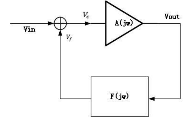
Figure 2: General Feedback System Diagram
Where \( A(jω) \) is the open-loop transfer function of the feedforward network, and \( F(jω) \) is the feedback function of the feedforward network, \( H(jω)=A(jω)∙F(jω) \) is the loop gain. The necessary but not sufficient conditions for oscillation in a feedback system can be represented by the Barkhuasen criterion below.
\( |H(jω)|≥1 \) (5)
\( ∠H(jω)=n∙{360^{∘}} (n=1,2,3…) \) (6)
By combining the above two conditions, this paper can deduce in reverse how the oscillation of the circuit occurs. In the circuit, noise with a frequency of \( {ω_{0}} \) is amplified and phase shifted by 360 ° through feedforward and feedback networks to obtain a signal with the same phase as the input signal. The feedback noise signal is added to the input signal to obtain a larger signal. In this way, the noise signal with a frequency of \( {ω_{0}} \) in the circuit is continuously amplified and regenerated. As the amplitude of the signal increases, the noise signal reaches the power supply voltage swing after passing through the nonlinearity of each stage of the circuit. When the loop oscillation is stable, \( H(jω) \) changes from greater than or equal to 1 to equal to 1.
The final oscillator outputs a signal with a frequency of 𝑤 0 and a swing of the power supply voltage. According to equations (5) and (6), it can be seen that when the feedback network is an amplifying circuit, if the feedback network is an attenuator, its attenuation value must not be greater than the gain of the feedforward network, and when the feedforward network is a capacitive circuit, the feedback network must be inductive.
The second method is to analyze through equivalent impedance, also known as the "negative impedance analysis method". According to the principle of oscillation circuit, oscillation circuit is generated by the alternating energy of inductance and capacitance. When the energy in inductance and capacitance alternates in the circuit, the flowing resistance will cause the electrical energy in the circuit to be continuously thermally lost. The solution is to add a circuit or device that can counteract the resistance effect to the circuit. From the above description, it can be seen that the oscillation circuit can be completely analyzed solely through equivalent impedance analysis of the circuit [5].
3.2. Crystal oscillator
Normally, feedforward networks are capacitive amplification circuits, and according to the oscillation conditions of the oscillation circuit, it is necessary to find inductors and capacitive amplifiers to form an oscillation loop. Quartz crystal, a stable hexagonal pyramidal crystal composed of silicon dioxide (𝑆𝑖𝑂 2) molecules. The fundamental reason why crystals can produce oscillations is their piezoelectric effect, where mechanical and electrical energy can be converted into oscillations within the crystal. When pressure is applied to the crystal surface, there will be a change in voltage at both ends of the surface. Similarly, applying a voltage crystal at both ends of the opposite surface will also generate mechanical vibration. When the frequency of the externally applied voltage signal is equal to the mechanical resonance frequency inside the crystal, the crystal will oscillate, and the conversion efficiency of electrical energy and mechanical energy is highest at the resonance frequency. The thinner the thickness of the crystal, the higher the resonant frequency [6, 7]. And quartz crystals can produce different natural frequencies, frequency temperature characteristics, etc. through different cutting types. From the perspective of development process, X, AT, GT, IT, PT, FC, SC, etc. have been invented successively, and their differences lie in cutting methods and corner sizes. Different cutting types are suitable for different design environments. Among them, the AT cut quartz crystal has been developed early and widely used, because it is insensitive to temperature changes and has the characteristics of high accuracy and good sensitivity.
3.3. Pierce oscillator
Due to the fact that the conditions for oscillator oscillation require an inductor and a capacitive amplifier to form the oscillator structure, where quartz crystal can be equivalent to an inductor, the other part of the capacitive amplifier that forms the loop can be completed by a single tube, and the more complex the structure, the more complex the function. When a single COMS tube can form a capacitive amplification circuit, an amplification circuit built with more tubes can also achieve this function.
In practical circuit design, a single tube crystal oscillator can derive three different oscillation circuits by setting different grounding points. They are Pierce oscillator [8-11], Colpitts oscillator [12, 13], and Santos oscillator. The Pierce oscillator is a single transistor source grounded, as shown in the figure 3.
Figure 3: Pierce oscillator
The output of a Pierce oscillator can be obtained from the drain or source, because when the circuit resonates, the energy of the capacitor and inductor cancel each other out, and the quartz crystal can be equivalent to a very small positive resistor. Therefore, the voltage between the drain and gate of a single transistor can be equivalent to 0. And the gate of the single transistor of the Colpitz oscillator is grounded to the quartz crystal, so that both the gate and drain of the transistor are grounded, so it can only output at the source level of the transistor. The Santos oscillator is a single transistor with its drain connected to ground, where the drain and gate potentials of the transistor are equivalent to ground, and the output can only be at the source level.
4. Design of Digital Real time Clock
4.1. Overall introduction of digital real-time clock
The main functions of the digital real-time clock designed this time include time output, date output, alarm clock, and other functions [14]. The input of the module includes an external crystal oscillator clock input with a low-frequency clock of 32KHz and an internal clock of the system with a frequency of 4MHz [15]. This module mainly consists of four parts: frequency division and frequency correction module, control module, clock main module, and display module.
4.2. Introduction to each module
4.2.1. SPI interface module
There are interface protocols in communication. An interface can be defined as a shared boundary used for exchanging information between software, computer hardware, or peripheral devices. On the other hand, protocols are typically defined as all objects that communicate unrelated to each other. In fact, the meaning of interface protocol is to exchange information between objects for mutual communication and understanding. The data transmission interface of the RTC chip in this article adopts Serial Peripheral Interface (SPI), and the SPI protocol will be introduced next.
Each SPI system consists of a master and one or more slaves, where the master is defined as the microcomputer that provides the clock for SPI, and the slave is any integrated circuit that receives the SPI clock from the master. A system can have multiple masters, but at any given time there can only be one master. SPI is a synchronous, full duplex communication bus that is more suitable for high-speed data transmission [16]. SPI can achieve higher transmission data rates, limited to 400KHz, with a compatible interface frequency range typically of 10MHz, but it typically serves multiple slavers. SPI does not define any speed limit, and its actual speed usually exceeds 10Mb/s [17].
4.2.2. Frequency divider
The function of the frequency division module in RTC is mainly to provide a reference clock clk_1 with a frequency of 1Hz for the main functional module, the perpetual calendar module, and to generate clock pulses of multiple frequencies. The input of this module is the output signal of the crystal oscillator - the 32.768KHz clock signal clk_32768, and the output signal is the 1Hz clock signal clk_1.
4.2.3. Perpetual Calendar Module
The perpetual calendar module is the main functional module in RTC, which is implemented asynchronously based on the Link Joint self-timing system. This module mainly completes basic calculation functions such as seconds, minutes, hours, days, weeks, months, and years. Through the SPI interface, it can transmit time data from seconds to years (lower two digits) with the MCU. It supports switching between 12 hour and 24 hour systems, and can automatically recognize leap years and normal years. That is, when the lower two potentials of a year are divided by 4, the year is a leap year.
An asynchronous RTC perpetual calendar module circuit designed based on the Link Joint self-clock system, with clk_1hz as the reference clock, can be used in conjunction with synchronous clock frequency to complete related tasks, including second timing circuit, minute timing circuit, hour timing circuit, day timing circuit, week timing circuit, month timing circuit, and year timing circuit.
The calendar module is only designed to work in conjunction with the synchronous clock, so clk_1hz is used as the reference clock. In fact, there is no global clock in the entire circuit, which can reduce the power consumption of high-frequency clock flipping compared to the synchronous circuit; For example, in a synchronous circuit, whether it is a minute timer circuit, hour timer circuit, day timer circuit, month timer circuit, or year timer circuit, they will all follow the clock clk_1hz
The rising edge works together with the second timing circuit, while in this asynchronous perpetual calendar module, the minute timing circuit only works once a minute, the hour timing circuit only works once an hour, the day timing circuit works once a day, the month timing circuit works once a month, and the year timing circuit works once a year. From this, this paper can see the advantages of using this asynchronous circuit design method in the perpetual calendar module [18].
4.3. Power consumption optimization in front-end design
The first method is to select a low power RTC module and the key is to choose RTC modules with ultra-low power consumption characteristics. Some high-performance RTC modules can operate at full speed with power consumption as low as tens of nanoamps (nA), which is crucial for maintaining time while reducing overall system power consumption. It can also compare the power consumption of RTC integrated into a microcontroller (MCU) with that of an external independent RTC. Usually, external RTC has lower power consumption as it can operate independently of MCU and continue to run even when MCU enters low-power mode.
Another method is Precise control of clock signal. Reduce power consumption by turning off the clock signal of the RTC module when it is not needed to operate. This can be achieved through software or hardware logic. It is also possible to optimize the position of the crystal oscillator by placing it as close as possible to the RTC module and using a ground layer to avoid interference from other circuits. This helps reduce signal loss and power consumption.
5. Conclusion
The first part of this paper's main work is to introduce the Theoretical Basis Analysis of Digital Low Power Technology, which mainly includes the following content: Composition of Power Consumption in CMOS Integrated Circuits, and the resulting low power technologies, as well as Chip System Architecture. The second part is an introduction to oscillators, mainly including basic principles and two special oscillators, Crystal oscillator and Pierce oscillator. Finally, the overall introduction of digital real-time clock was introduced, which includes SPI interface module, frequency divider, and Perpetual Calendar module. Finally, power consumption optimization in front-end design was introduced.
With the rapid development of the Internet of Things, smart homes, and smart offices, the demand for low-power, high-precision, and real-time clocks is constantly increasing. Low power digital real-time clocks have significant advantages in these fields and can meet the needs of long-term device operation and precise time synchronization. Therefore, it can be foreseen that the market demand for low-power digital real-time clocks will continue to grow in the future. The application scenarios of low-power digital real-time clocks will continue to expand, from traditional areas such as homes, schools, and offices to a wider range of fields. For example, in intelligent transportation systems, low-power digital real-time clocks can be used for vehicle positioning and time synchronization; In the field of industrial automation, it can be used for time control and synchronization on production lines; In the medical field, it can be used for time recording and synchronization of medical equipment. The expansion of these application scenarios will further promote the development of low-power digital real-time clocks.
References
[1]. Shanghai Dongju Electronics Co., Ltd Development History and Current Status of Real time Clock Integrated Circuits: Electrical Measurement and Instrumentation, 2021, 58 (10): 32-34
[2]. Venkatesh G, Hamid M, Vazgen M, et al. Low Power Design Flow Based on Unified Power Format and Synopsys tool chain. IEEE 2013 3rd Interdisciplinary Engineering Design Education Conference,4-5 March 2013
[3]. Chi L. Design and Implementation of Low Power Digital Real time Clock. Xi'an University of Electronic Science and Technology, 2019.
[4]. Frank E, Mark B. Power Reduction Reduction through RTL. Clock Gating. S NUG, 2005, 5: 29-31
[5]. Jie H. Design of a low-power digital temperature compensation real-time clock chip. University of Electronic Science and Technology of China, 2022.
[6]. HμAng Q, Neubig B, Wu Z, et al. Analysis of Vibrations of Circular QμArtz Crystal Resonators for Sensor Applications. 2020 IEEE International Ultrasonics Symposiμm (IUS), 2020, 1-3.
[7]. Uchiki S, Sato I, Sohgawa M, et al. Design and EvalμAtion of an Electrode Separated QμArtz Crystal Microbalance Array as a Disposable Weighing Dish. 2019 20th International Conference on Solid-State Sensors, ActμAtors and Microsystems & Eurosensors XXXIII, 2019, 1169-72
[8]. Chengjie Z, Sinha N, Spiegel J V D, et al. Multi-frequency pierce oscillators based on piezoelectric AlN contour-mode MEMS resonators. 2008 IEEE International Frequency Control Symposiμm, 2008, 402-7.
[9]. Farahvash S, Quek C, Mak M. A Temperature-Compensated Digitally-Controlled Crystal Pierce Oscillator for Wireless Applications. 2008 IEEE International Solid-State Circuits Conference - Digest of Technical Papers, 2008, 352-619.
[10]. Hamzah M H M, Nordin A N, Karim J. Low power and high voltage swing cascode Pierce oscillator for MEMS SAW resonators. 2016 Symposiμm on Design, Test, Integration and Packaging of MEMS/MOEMS (DTIP), 2016, 1-4.
[11]. Karim J, Nordin A N, Alam A Z. Design of a pierce oscillator for CMOS SAW resonator. 2012 International Conference on Computer and Communication Engineering (ICCCE), 2012, 490-3.
[12]. Imani A, Hashemi H. Frequency and Power Scaling in mm-Wave Colpitts Oscillators. IEEE Journal of Solid-State Circuits, 2018, 1338-47.
[13]. Nomura N, Aoyagi Y, Chang C, et al. A Colpitts-Type Crystal Oscillator for Gigahertz Frequency. 2006 IEEE International Frequency Control Symposiμm and Exposition, 2006, 233-6.
[14]. Gendai L. Research and Design of Calibratable Real time Clock Chip. Huazhong University of Science and Technology, May 2007
[15]. Texas Instruments Inc. DP8573A Real Time Clock (RTC). Texas Instruments Inc,2011
[16]. Saha S, Rahman M A, Thakur A. Design and implementation of SPI bus protocol with Built-in-self-test capability over FPGA. 2014 International Conference on Electrical Engineering and Information & Communication Technology. IEEE, 2014: 1-6.
[17]. Srinivas A, Kumar M K, Bhandari J K. Design and verification of serial peripheral interface[J]. International Journal of Engineering Development and Research, 2014, 1(3): 130-136-130-136.
[18]. Mengya W. Design and Implementation of Low Power Digital Real Time Clock Based on Asynchronous Circuit. Hunan University, 2022.
Cite this article
Wang,M. (2025). Analysis and Design of Low Power Digital Real Time Clock. Applied and Computational Engineering,127,73-81.
Data availability
The datasets used and/or analyzed during the current study will be available from the authors upon reasonable request.
Disclaimer/Publisher's Note
The statements, opinions and data contained in all publications are solely those of the individual author(s) and contributor(s) and not of EWA Publishing and/or the editor(s). EWA Publishing and/or the editor(s) disclaim responsibility for any injury to people or property resulting from any ideas, methods, instructions or products referred to in the content.
About volume
Volume title: Proceedings of the 5th International Conference on Materials Chemistry and Environmental Engineering
© 2024 by the author(s). Licensee EWA Publishing, Oxford, UK. This article is an open access article distributed under the terms and
conditions of the Creative Commons Attribution (CC BY) license. Authors who
publish this series agree to the following terms:
1. Authors retain copyright and grant the series right of first publication with the work simultaneously licensed under a Creative Commons
Attribution License that allows others to share the work with an acknowledgment of the work's authorship and initial publication in this
series.
2. Authors are able to enter into separate, additional contractual arrangements for the non-exclusive distribution of the series's published
version of the work (e.g., post it to an institutional repository or publish it in a book), with an acknowledgment of its initial
publication in this series.
3. Authors are permitted and encouraged to post their work online (e.g., in institutional repositories or on their website) prior to and
during the submission process, as it can lead to productive exchanges, as well as earlier and greater citation of published work (See
Open access policy for details).
References
[1]. Shanghai Dongju Electronics Co., Ltd Development History and Current Status of Real time Clock Integrated Circuits: Electrical Measurement and Instrumentation, 2021, 58 (10): 32-34
[2]. Venkatesh G, Hamid M, Vazgen M, et al. Low Power Design Flow Based on Unified Power Format and Synopsys tool chain. IEEE 2013 3rd Interdisciplinary Engineering Design Education Conference,4-5 March 2013
[3]. Chi L. Design and Implementation of Low Power Digital Real time Clock. Xi'an University of Electronic Science and Technology, 2019.
[4]. Frank E, Mark B. Power Reduction Reduction through RTL. Clock Gating. S NUG, 2005, 5: 29-31
[5]. Jie H. Design of a low-power digital temperature compensation real-time clock chip. University of Electronic Science and Technology of China, 2022.
[6]. HμAng Q, Neubig B, Wu Z, et al. Analysis of Vibrations of Circular QμArtz Crystal Resonators for Sensor Applications. 2020 IEEE International Ultrasonics Symposiμm (IUS), 2020, 1-3.
[7]. Uchiki S, Sato I, Sohgawa M, et al. Design and EvalμAtion of an Electrode Separated QμArtz Crystal Microbalance Array as a Disposable Weighing Dish. 2019 20th International Conference on Solid-State Sensors, ActμAtors and Microsystems & Eurosensors XXXIII, 2019, 1169-72
[8]. Chengjie Z, Sinha N, Spiegel J V D, et al. Multi-frequency pierce oscillators based on piezoelectric AlN contour-mode MEMS resonators. 2008 IEEE International Frequency Control Symposiμm, 2008, 402-7.
[9]. Farahvash S, Quek C, Mak M. A Temperature-Compensated Digitally-Controlled Crystal Pierce Oscillator for Wireless Applications. 2008 IEEE International Solid-State Circuits Conference - Digest of Technical Papers, 2008, 352-619.
[10]. Hamzah M H M, Nordin A N, Karim J. Low power and high voltage swing cascode Pierce oscillator for MEMS SAW resonators. 2016 Symposiμm on Design, Test, Integration and Packaging of MEMS/MOEMS (DTIP), 2016, 1-4.
[11]. Karim J, Nordin A N, Alam A Z. Design of a pierce oscillator for CMOS SAW resonator. 2012 International Conference on Computer and Communication Engineering (ICCCE), 2012, 490-3.
[12]. Imani A, Hashemi H. Frequency and Power Scaling in mm-Wave Colpitts Oscillators. IEEE Journal of Solid-State Circuits, 2018, 1338-47.
[13]. Nomura N, Aoyagi Y, Chang C, et al. A Colpitts-Type Crystal Oscillator for Gigahertz Frequency. 2006 IEEE International Frequency Control Symposiμm and Exposition, 2006, 233-6.
[14]. Gendai L. Research and Design of Calibratable Real time Clock Chip. Huazhong University of Science and Technology, May 2007
[15]. Texas Instruments Inc. DP8573A Real Time Clock (RTC). Texas Instruments Inc,2011
[16]. Saha S, Rahman M A, Thakur A. Design and implementation of SPI bus protocol with Built-in-self-test capability over FPGA. 2014 International Conference on Electrical Engineering and Information & Communication Technology. IEEE, 2014: 1-6.
[17]. Srinivas A, Kumar M K, Bhandari J K. Design and verification of serial peripheral interface[J]. International Journal of Engineering Development and Research, 2014, 1(3): 130-136-130-136.
[18]. Mengya W. Design and Implementation of Low Power Digital Real Time Clock Based on Asynchronous Circuit. Hunan University, 2022.