


1. Introduction
Since being invented using first-generation materials like Silicon (Si) and Gallium (Ga) in the 1800s, power electronics have kept evolving and iterating generations to seek higher reliability, performance, and cost-efficiency. To address the limits in all high-power and high-temperature applications of first-generation materials, semiconductors using compound or ternary compounds were introduced to enable high power density, high-frequency response, and high thermal dissipation devices. In recent decades, wide band gap (WBG) semiconductors including silicon carbide (SiC) and gallium nitrate (GaN) have developed in the manufacture of power electronics, marking another significant leap from traditional silicon-based devices. They have played a critical role in the production of devices because of their high-power endurance, faster switching speed, and greater thermal efficiency.
However, with the relentless demand for higher performance and cost-efficiency, the exploration of ultra-wide bandgap (UWBG) materials further boosts the development of semiconductors, resulting in the emergence of 4th-generation power electronics. These ultra-wide bandgap materials include Gallium Oxide (Ga₂O₃), diamond, and aluminum nitride (AlN). Among all of them, gallium oxide (Ga₂O₃) stands out due to its extraordinary physical properties, including an exceptionally wide band gap of approximately 4.8 eV, a high breakdown electric field of approximately 8 MV/cm*K, and the capability to fabricate large single-crystal wafers at low expense using mature melt-based methods. These unique attributes render Ga₂O₃ highly promising for high-voltage, high-power, and harsh-environment applications [1]. Ga₂O₃ exists in five polymorphs—designated as α, β, γ, δ, and ε phases—each offering unique structural and electronic properties. While other phases can also be applied in some specific regions, β-Ga₂O₃ appeals to the most attention because it is the most stable and widely studied phase, crystallizing in a monoclinic structure [2]. The melt-based methods that allow large-scale crystal growth also lie in this phase, making it highly possible to be the primary candidate for 4th-generation power electronics.
However, though the potential of β-Ga₂O₃ is undeniable, significant challenges remain in the its material science, especially in the fabrication of effective p-type semiconductor. While the n-type doping of Ga₂O₃ has been successfully established using donor impurities like silicon (Si) and tin (Sn), which exhibit high activation rates and broad variation in electron concentrations, p-type doping persists in difficulties due to the fundamental material constraints of Ga₂O₃.The limitations such as the presence of deep acceptor levels and the inherently poor mobility of holes result from the flatness of the valence band of Ga₂O₃. With the existence of these limited physical properties, Ga₂O₃ becomes energetically unfavorable for conventional acceptor dopants to activate efficiently, leading to low carrier concentrations and high resistivity in doped layers [3]. The challenges of p-type doping are also caused by the self-trapping of holes, a phenomenon where lattice distortions around the hole localize and prevent the hole from contributing effectively to conduction. These intrinsic obstacles not only hinder the development of essential bipolar devices like p-n junctions and light-emitting diodes but also restrict the applicability of the material in advanced electronic architecture that requires both n-type and p-type regions for optimal performance [4].
Efforts to address these challenges have explored various unconventional doping strategies, such as introducing deep acceptors like magnesium (Mg), nitrogen (N), and zinc (Zn), as well as employing co-doping techniques to improve dopant activation. Despite some progress, these methods often result in some unavoidable trade-offs, such as reduced stability or difficulty in maintaining scalability for industrial applications. Methods like using heterojunctions that leverage the difference in electronic properties between two different semiconductor materials are also a possible general solution to the difficult p-type doping of β-Ga₂O₃ [5].
This paper aims to comprehensively address the current state of p-type doping in β-Ga₂O₃, a critical challenge in the development of this promising ultra-wide bandgap material. It begins by examining the various existing methods employed for p-type doping, ranging from conventional approaches like Mg and N doping to more advanced techniques such as co-doping strategies and heterojunction methods. These methods will be introduced in detail to explicate their underlying mechanisms and the possibility of effectiveness in overcoming the constraints of β-Ga₂O₃. The paper will consequently provide a comparative evaluation and analysis of these doping techniques to highlight their advantages and limitations to finally point out a respective more suitable general solution for the p-type doping of β-Ga₂O₃.
2. Design & Fabrication
Because of the intrinsic properties such as wide band gap and electron structure that result in the deep acceptor levels and limited hole mobility, the p-type doing of β-Ga₂O₃ becomes a significant challenge for its further use in electronic devices. As a result, the goal of designing the p-type doping of β-Ga₂O₃ is to modify its conductivity and enable the fabrication of both unipolar and bipolar devices. To address such intrinsic challenges of β-Ga₂O₃, various doping strategies are explored to introduce effective p-type carriers into the crystal lattice.
2.1. Single Element Doping
This traditional approach introduces a single type of dopant into the β-Ga₂O₃ lattice to modify its electrical behavior. For p-type doping, elements such as Mg, Zn, and N are considered potential candidate due to their probability to introduce holes into the structure of Ga₂O₃-based semiconductor, enabling p-type conductivity. Mg and Zn have such potential because they are both group II elements, which are similar to the gallium inside β-Ga₂O₃. By substituting for gallium in the lattice, the Ga₂O₃-based semiconductor is expected to be introduced hole as Mg and Zn both have one less electron than gallium. N is considered to have such potential because it is a group V element that can occupy oxygen sites in the lattice, producing a mid-gap acceptor state.
2.2. Co-doping
Co-doping involves the use of a combination of dopants to manipulate the electronic properties of β-Ga₂O₃ more effectively. By co-doping two different dopants into the nanostructure of β-Ga₂O₃ through some methods like hydrothermal synthesis, the activation energy for acceptor dopants can be potentially diminished.
2.3. Heterojunction
Because it is difficult to make effective p-type conductivity using conventional doping methods, heterojunction approaches are raised to solve such problems that bipolar devices are currently not available to be fabricated. Instead of creating a p-type β-Ga₂O₃-based semiconductor, band alignments between n-type β-Ga₂O₃ and another p-type material are implemented in heterojunction approaches. Through these methods, the p-type characteristics of the other material can be effectively used to solve the p-type conductivity problem while the semiconductor can still benefit from the high breakdown voltage and electron mobility of n-type β-Ga₂O₃.
3. Analysis & Challenge
3.1. Single Element Doping
While the research on the feasibility of p-type doping in β-Ga₂O₃ using single-element doping is extensive, most of them have shown this approach had limited effectiveness in achieving practical p-type doping for β-Ga₂O₃. Among all main-group elements, various cationic substitutional dopants have been considered to induce p-type conductivity including lithium (Li), sodium (Na), potassium (K), beryllium (Be), magnesium (Mg), calcium (Ca), copper (Cu), gold (Au), and zinc (Zn), but they all remain intrinsic material limitations that prevent effective doping.
The elements were selected because of their potential to occupy gallium sites within the lattice and behave as acceptors. In order to find out whether they could act as practical p-type dopants for β-Ga₂O₃, advanced computational techniques, specifically density functional theory (DFT) including both generalized gradient approximation (GGA) and hybrid functional calculations (HSE), were utilized to predict the electronic properties of these dopants in the β-Ga₂O₃ lattice. Inside GGA, the popular Perdew-Burke-Ernzerhof (PBE) model was used to estimate the interaction of dopants with the lattice, providing a cost-effective method to predict the formation energies and transition levels of defects. Moreover, due to its limitations in accurately predicting band gaps, HSE is incorporated to make the result more precise. Both methods employ the projector augmented wave (PAW) method, aiming to identify whether the p-type dopants could introduce shallow acceptor levels close to the valence band [6].
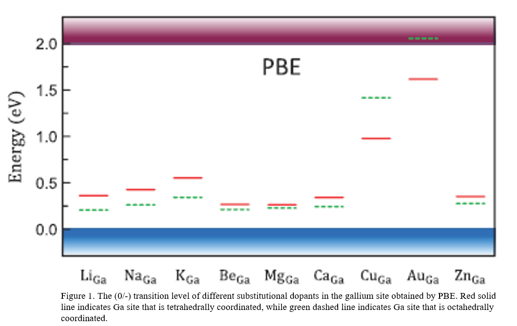
Figure 1: Transition levels for different dopants of gallium, which is calculated by PBE as shown on the graph. The red line in the graph indicates a tetrahedrally coordinated Ga site while the green line indicates an octahedrally coordinated Ga Site. The blue region indicates valence band while blue region indicates conduction band.[6]
By examining Figure 1, it can be seen that all dopant candidates suggested deep acceptor levels because their transition levels that indicates where dopants could accept an electron are far above the valence band maximum (VBM). As a result, due to these deep levels, these dopants could not effectively contribute to p-type conductivity because the energy required to ionize the dopants and generate free holes is prohibitively high.
However, unlike other dopants, N stood out as the most promising single dopant for β-Ga₂O₃ due to its unique ability to create a shallower acceptor levels near the VBM in recent study. When nitrogen substitutes the oxygen of β-Ga₂O₃ during the thermal oxidation process, it introduces acceptor levels with a significant low ionization energy of about 0.087 eV. Such low ionization energy allows an easier activation of free holes compared to other single dopants like Mg, Ve, or Cu.
To fabricate the p-type β-Ga₂O₃-based film, N₂O was used as the oxidation ambient to incorporate the nitrogen into β-Ga₂O₃ because the low bond energy of N-O in the N₂O molecule made the incorporation during the growth process more efficient. The thermal oxidation of GaN at 1100°C led to the formation of a unique two-layer structure in the β-Ga₂O₃ films. As shown in Figure 2, while the top layer consisted of loosely arranged nanorods, the second layer beneath it was comparatively dense and compact, providing a stable base with high p-type conductivity. This improved remarkable p-type conductivity was demonstrated by the high hole concentration of 1.64*10^17 cm^-3 and low resistivity of 7.66 Ω·cm, making the film to be a promising material for advanced optoelectronic applications [7].
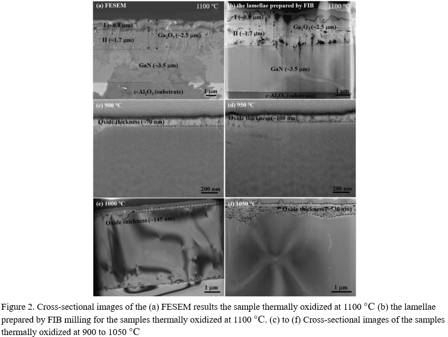
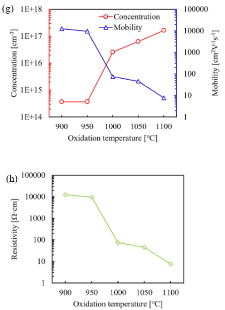
Figure 2: (a) cross-sectional image of N-doped β-Ga₂O₃ under 1100°C using method of thermal oxidation of GaN in N2O ambient, resulted from FESEM, (b) cross-sectional image of the same sample under same temperature used the lamellae prepared by FIB to observe, (c) to (f) cross- sectional image of the same sample thermally oxidized at 900°C, 950°C, 1000°C, and 1050°C, (g) Hall mobility and concentration of N-doped β-Ga₂O₃ varied from 900 to 1100°C, and (h) Hall resistivity of the sample varied from 900 to 1100°C [7]
3.2. Co-doping
Because single element doping have shown the imitation in p-type conductivity caused by deep acceptor level, co-doping using appropriate element combos became a reasonable strategy to deal with the difficulty in p-type doping of β-Ga₂O₃. Under this context, multiple co-dopants were applied in practice such as Zn-Mg co-doping in β-Ga₂O₃ thin films. These films were fabricated using radio frequency (RF) magnetron sputtering with a high-purity Ga₂O₃ target embedded with ZnO and MgO pieces, followed by annealing at 600 °C in a N₂ atmosphere to improve crystallinity and dopant incorporation. The product was shown in Figure 3(a). The co-doping of with Zn and Mg resulted in the polycrystalline films with acceptor levels at 0.79 eV for Zn part and 1.00 eV for Mg part above the VBM. This result showed that the introduction of the additional acceptor level did slightly improve the doping efficiency and modulated the material’s bandgap compared to single element doping [8]. As shown in Figure 3(b), while singe Zn doping to β-Ga₂O₃ only create a bandgap of 4.88 eV, the Zn-Mg co-doping increases the bandgap to 5.08 eV due to the higher bandgap of about 7.8 eV of MgO. However, such acceptor levels were still too deep to enable effective p-type conductivity at room temperature because the activation energy required to ionize these levels and generate free holes remains too high. Consequently, though co-doping offered certain improvement in structural and optical properties for β-Ga₂O₃-based semiconductor, it was not sufficient to address the fundamental challenge of achieving low resistivity and high hole concentration. As the resulting semiconductors still lacked the necessary p-type conductivity that can be used in high-performance power electronics, the Zn-Mg co-doping method was not effective enough for the fabrication of p-type β-Ga₂O₃-based semiconductor.
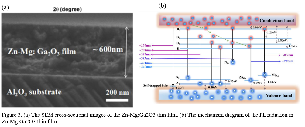
Figure 3: (a) The cross-sectional images of the co-doping Ga2O3 thin film using Zn and Mg, resulted from SEM, and (b) the band diagram of the PL radiation in Ga2O3 thin film using Zn and Mg as co-dopants[8]
Zn-Mg co-doping represented the epitome of all potential co-dopants. While this co-doping method slightly decreased the deep acceptor level in β-Ga₂O₃ toward the VBM by reducing the lattice distortion and self-compensation effects in β-Ga₂O₃ doping, it was still insufficient for achieving practical p-type conductivity. However, while semiconductor with co-doping such as Zn-Mg, Al-N, and In-N were all attested that they have insufficient p-type conductivity, some other potential co-dopants such as N-Mg and N-Zn that can be further investigated to ensure whether they can fabricate β-Ga₂O₃ semiconductor with enough p-type conductivity [9].
3.3. Heterojunction
The development of heterojunction provided an alternate method to solve the difficulty in p-type doping and conductivity of β-Ga₂O₃. Instead of finding a dopant to dope with β-Ga₂O₃ to create a p-type β-Ga₂O₃, heterojunction approaches utilized the mature n-type doping methods of β-Ga₂O₃ combined with other easier-doped p-type materials to create heterojunction devices, thus overcoming the limitations of homojunction in β-Ga₂O₃. while bipolar devices could be fabricated though this technique, devices can also inherited the UWBG property of β-Ga₂O₃, such as SiC/β-Ga₂O₃, and NiO/β-Ga₂O₃ heterojunctions [10]. Among these heterojunctions, the NiO/β-Ga₂O₃ heterojunction showed a higher potential because NiO had a wider bandgap and higher p-type conductivity compared to other components. A common heterojunction device based on NiO/β-Ga₂O₃ could reach a breakdown voltage of 4.7 kV, 5.2 GW/cm^2 BFOM, and could maintain stable optimized performance until 275 °C. This excellent performance was facilitated by the effective band alignment at the NiO/β-Ga₂O₃ interface, which enhances electron injection from β-Ga₂O₃ into NiO. By modifying the growth and fabrication method, the performance of the heterojunction could be further enhanced.
For example, a typical vertical heterojunction p-NiO/n-β-Ga₂O₃ diodes was shown in Figure 4, NiO/β-Ga₂O₃ heterojunction achieved a stable optimized performance up to 410 °C by using special growth and fabrication methods. To create the heterojunction, pulsed laser deposition (PLD) was used to grow textured polycrystalline p-NiO layers on single-crystal n-type β-Ga₂O₃ without any drift layer, patterned using a reactive ion etch (RIE) process, subjected to a high-temperature annealing step. Compared to other Ga₂O₃-based devices, NiO/β-Ga₂O₃ heterojunction diodes under this design achieved a diode on-off ratio of more than 10^6 up to 410 °C due to the increased build-in voltage and additional band offset of the p-n heterojunction diode, indicating the excellent performance of the diode under high-temperature circumstance [11].
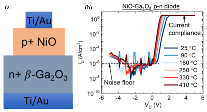
Figure 4: (a) Structure of vertical heterojunction diodes using p-type NiO and n-type β-Ga₂O₃ as semiconductor materials and Ti or Au as metal. (b) I-V graph of vertical heterojunction diodes using p-type NiO and n-type β-Ga₂O₃. The diodes show improved high-temperature behavior. The measurement is done on 200 μm contact pads with 1 mA current compliance, where the noise floor corresponds to 10-6 A cm-2 [13]
This kind of improvement demonstrated the significant potential of heterojunction in solving the p-type doping problem of β-Ga₂O₃ because heterojunction bipolar devices with high performance have already been created and there is a clear indication for continued advancements. For example, while thermal stability is improved by NiO with special growth and fabrication methods, there is the possibility to further improve it using SiC which has optimized performance up to 600 °C in p-i-n configuration. Moreover, the challenges of interface quality and scalability problems also require to be overcome because leakage current should be continuously reduced by improving interface quality and methods like PLD and RIE still have technological and economic difficulties to overcome to achieve scalability.
4. Suggestion
To overcome the challenge of achieving practical p-type conductivity in β-Ga₂O₃, single-element doping, co-doping, and heterojunction approaches are introduced. Advantages and disadvantages were concluded and shown in Table 1. Each method offers unique advantages and limitations, influencing their applicabilities to β-Ga₂O₃-based semiconductors.
Table 1: Comparison the advantage, disadvantage and potential application for p-type doping of β-Ga₂O₃
Method | Advantages | Disadvantages | Potential in application |
Single element doping | -Simple implementation -Shallower acceptor level | -Deep acceptor levels -Self-compensation effects; -Poor hole mobility; -Low conductivity. | -Limited application. |
Co-doping | -Improved doping efficiency; -Capable to modulate bandgap; -Capable to reduce lattice distortion effects. | -Deep acceptor levels -Low conductivity at room temperature. | -Own marginal improvement but not practical. |
Heterojunction | -Effectively bypass the p-type doping challenge; -Excellent performance. | -Insufficient scalability -Inadequate interface quality. -Diminishing leakage currents remain challenges; -Need to depend on external p-type materials. | -Highly promising for bipolar devices -Suitable for applications. |
From the Table 1, it can be observed that heterojunction is the current most promising method in solving the p-type doping of β-Ga₂O₃. Such result is plausible because the intrinsic properties of β-Ga₂O₃, including its deep acceptor levels, self-compensation effects, and poor hole mobility, all make it unfavorable for conventional p-type doping methods, whereas heterojunctions bypass these limitation by utilizing an external p-type material to achieve the fabrication of bipolar devices that contains the UWBG property of β-Ga₂O₃. Comparatively, the semiconductor fabricated through single-element doping and co-doping methods both show limited properties because of the deep acceptor level.
However, the success of heterojunction and challenge inside single element doping and co-doping methods does not indicate their uselessness. While some novel dopant combinations like N-Mg and N-Zn can be further investigated to potentially create shallower acceptor levels in co-doping method, single element doping using N as the dopant also shows a relatively better performance due to its ability to create shallower acceptor levels near VBM. These discoveries and assumptions show the potential of both methods that allows further research.
Moreover, there are also plenty of challenges that heterojunction approaches need to overcome. One major challenge is the interface quality between β-Ga₂O₃ and the external p-type material, which poor one can result in the high leakage currents and reduction of device efficiency. The thermal and chemical mismatch between β-Ga₂O₃ and the p-type material also introduce structural defects, further degrading performance. Another significant issue is scalability, which current fabrication techniques like PLD and RIE are expensive and difficult to implement on an industrial scale.
In order to solve these challenges, while improving interface engineering, optimizing the heterojunction structure, and exploring new scalable fabrication methods are all important, applying hybrid methods of heterojunction and single element doping or co-doping are also potentially useful.
5. Conclusion
In conclusion, though β-Ga₂O₃ is a promising material with unique properties such as UWBG and high breakdown electric field, and potential cost-effective growth method for power electronics and optoelectronic applications of next generation, achieving a practical p-type conductivity for its semiconductor remains challenging. This paper explored and compared three primary approaches to address this challenge: single element doping, co-doping, and heterojunction methods. While single element doping has been extensively studied, its effectiveness is strictly impaired by the intrinsic limitation of β-Ga₂O₃ such as flat valence band, self-trapping effect, and poor hole mobility. Though some dopants show a potential that can be further investigated, most single element dopants show a deep acceptor level that results in poor p-type conductivity. Similarly, co-doping offer slight improvements in structural and optical properties of β-Ga₂O₃-based semiconductor by modulating the bandgap and reducing the lattice distortion. However, such improvement is still insufficient to achieve practical p-type conductivity. On the contrary, heterojunction approaches become the most promising methods among these three. By bypassing the inherent limitation of β-Ga₂O₃, heterojunction approaches integrate n-type β-Ga₂O₃ with an external p-type materials to achieve the fabrication of bipolar devices and integrate the UWBG advantage of β-Ga₂O₃. The fabricated devices show significant performance advantages such as high breakdown voltage and thermal stability. However, interface quality, scalability and leakage currents of heterojunction devices remain challenging. To overcome these persistent limitations among all methods, future research should focus on advanced co-doping strategies using novel combinations of dopants, intrinsic defect engineering that can improve the interface quality, and hybrid methods that can potentially combine heterojunction approaches with other doping methods. Overall, while significant challenges remain, ongoing advancements in p-type doping strategies and heterojunction technologies provide a clear path for future research to investigate. With continuous innovation, β-Ga₂O₃ can become a concrete foundation for next-generation electronic devices.
References
[1]. Chikoidze, E., Fellous, A., Perez-Tomas, A., Sauthier, G., Tchelidze, T., Ton-That, C., Huynh, T. T., Phillips, M., Russell, S., Jennings, M., Berini, B., Jomard, F., & Dumont, Y. (2017). P-type β-gallium oxide: A new perspective for power and optoelectronic devices. Materials Today Physics, 3, 118–126. https://doi.org/10.1016/j.mtphys.2017.10.002
[2]. Galazka, Z. (2018). β-Ga2O3 for wide-bandgap electronics and Optoelectronics. Semiconductor Science and Technology, 33(11), 113001. https://doi.org/10.1088/1361-6641/aadf78
[3]. Qiao, R., Zhang, H., Zhao, S., Yuan, L., Jia, R., Peng, B., & Zhang, Y. (2022). A state-of-art review on gallium oxide field-effect transistors. Journal of Physics D: Applied Physics, 55(38), 383003. https://doi.org/10.1088/1361-6463/ac7c44
[4]. Higashiwaki, M., & Wong, M. H. (2024). Beta-gallium oxide material and device technologies. Annual Review of Materials Research, 54(1), 175–198. https://doi.org/10.1146/annurev-matsci-080921-104058
[5]. Mehta, M., & Avasthi, S. (2023). The possibility of gallium oxide (β-Ga2O3) heterojunction bipolar transistors. Physica Scripta, 98(2), 025013. https://doi.org/10.1088/1402-4896/acb325
[6]. Kyrtsos, A., Matsubara, M., & Bellotti, E. (2018). On the feasibility of P-type Ga2O3. Applied Physics Letters, 112(3). https://doi.org/10.1063/1.5009423
[7]. Liu, Y., Wei, S., Shan, C., Zhao, M., Lien, S.-Y., & Lee, M. (2022). Compositions and properties of high-conductivity nitrogen-doped P-type β-Ga2O3 films prepared by the thermal oxidation of gan in N2O ambient. Journal of Materials Research and Technology, 21, 3113–3128. https://doi.org/10.1016/j.jmrt.2022.10.110
[8]. Su, Y., Guo, D., Ye, J., Zhao, H., Wang, Z., Wang, S., Li, P., & Tang, W. (2019). Deep level acceptors of Zn-mg divalent ions dopants in β-Ga2O3 for the difficulty to P-type conductivity. Journal of Alloys and Compounds, 782, 299–303. https://doi.org/10.1016/j.jallcom.2018.12.199
[9]. Ma, J., Lin, J., Liu, J., Li, F., Liu, Y., & Yang, G. (2020). Achieving high conductivity P-type Ga2O3 through Al-N and in-N co-doping. Chemical Physics Letters, 746, 137308. https://doi.org/10.1016/j.cplett.2020.137308
[10]. Nakagomi, S., Hiratsuka, K., Kakuda, Y., & Yoshihiro, K. (2016). Beta-gallium oxide/sic heterojunction diodes with high rectification ratios. ECS Journal of Solid State Science and Technology, 6(2). https://doi.org/10.1149/2.0061702jss
[11]. Sohel, S. H., Kotecha, R., Khan, I. S., Heinselman, K. N., Narumanchi, S., Tellekamp, M. B., & Zakutayev, A. (2023). Gallium oxide heterojunction diodes for 400 °C high‐temperature applications. Physica Status Solidi (a), 220(20). https://doi.org/10.1002/pssa.202300535
Cite this article
Yin,B. (2025). A Review of the P-type Doping Method of Beta-gallium Oxide. Applied and Computational Engineering,117,210-219.
Data availability
The datasets used and/or analyzed during the current study will be available from the authors upon reasonable request.
Disclaimer/Publisher's Note
The statements, opinions and data contained in all publications are solely those of the individual author(s) and contributor(s) and not of EWA Publishing and/or the editor(s). EWA Publishing and/or the editor(s) disclaim responsibility for any injury to people or property resulting from any ideas, methods, instructions or products referred to in the content.
About volume
Volume title: Proceedings of the 3rd International Conference on Mechatronics and Smart Systems
© 2024 by the author(s). Licensee EWA Publishing, Oxford, UK. This article is an open access article distributed under the terms and
conditions of the Creative Commons Attribution (CC BY) license. Authors who
publish this series agree to the following terms:
1. Authors retain copyright and grant the series right of first publication with the work simultaneously licensed under a Creative Commons
Attribution License that allows others to share the work with an acknowledgment of the work's authorship and initial publication in this
series.
2. Authors are able to enter into separate, additional contractual arrangements for the non-exclusive distribution of the series's published
version of the work (e.g., post it to an institutional repository or publish it in a book), with an acknowledgment of its initial
publication in this series.
3. Authors are permitted and encouraged to post their work online (e.g., in institutional repositories or on their website) prior to and
during the submission process, as it can lead to productive exchanges, as well as earlier and greater citation of published work (See
Open access policy for details).
References
[1]. Chikoidze, E., Fellous, A., Perez-Tomas, A., Sauthier, G., Tchelidze, T., Ton-That, C., Huynh, T. T., Phillips, M., Russell, S., Jennings, M., Berini, B., Jomard, F., & Dumont, Y. (2017). P-type β-gallium oxide: A new perspective for power and optoelectronic devices. Materials Today Physics, 3, 118–126. https://doi.org/10.1016/j.mtphys.2017.10.002
[2]. Galazka, Z. (2018). β-Ga2O3 for wide-bandgap electronics and Optoelectronics. Semiconductor Science and Technology, 33(11), 113001. https://doi.org/10.1088/1361-6641/aadf78
[3]. Qiao, R., Zhang, H., Zhao, S., Yuan, L., Jia, R., Peng, B., & Zhang, Y. (2022). A state-of-art review on gallium oxide field-effect transistors. Journal of Physics D: Applied Physics, 55(38), 383003. https://doi.org/10.1088/1361-6463/ac7c44
[4]. Higashiwaki, M., & Wong, M. H. (2024). Beta-gallium oxide material and device technologies. Annual Review of Materials Research, 54(1), 175–198. https://doi.org/10.1146/annurev-matsci-080921-104058
[5]. Mehta, M., & Avasthi, S. (2023). The possibility of gallium oxide (β-Ga2O3) heterojunction bipolar transistors. Physica Scripta, 98(2), 025013. https://doi.org/10.1088/1402-4896/acb325
[6]. Kyrtsos, A., Matsubara, M., & Bellotti, E. (2018). On the feasibility of P-type Ga2O3. Applied Physics Letters, 112(3). https://doi.org/10.1063/1.5009423
[7]. Liu, Y., Wei, S., Shan, C., Zhao, M., Lien, S.-Y., & Lee, M. (2022). Compositions and properties of high-conductivity nitrogen-doped P-type β-Ga2O3 films prepared by the thermal oxidation of gan in N2O ambient. Journal of Materials Research and Technology, 21, 3113–3128. https://doi.org/10.1016/j.jmrt.2022.10.110
[8]. Su, Y., Guo, D., Ye, J., Zhao, H., Wang, Z., Wang, S., Li, P., & Tang, W. (2019). Deep level acceptors of Zn-mg divalent ions dopants in β-Ga2O3 for the difficulty to P-type conductivity. Journal of Alloys and Compounds, 782, 299–303. https://doi.org/10.1016/j.jallcom.2018.12.199
[9]. Ma, J., Lin, J., Liu, J., Li, F., Liu, Y., & Yang, G. (2020). Achieving high conductivity P-type Ga2O3 through Al-N and in-N co-doping. Chemical Physics Letters, 746, 137308. https://doi.org/10.1016/j.cplett.2020.137308
[10]. Nakagomi, S., Hiratsuka, K., Kakuda, Y., & Yoshihiro, K. (2016). Beta-gallium oxide/sic heterojunction diodes with high rectification ratios. ECS Journal of Solid State Science and Technology, 6(2). https://doi.org/10.1149/2.0061702jss
[11]. Sohel, S. H., Kotecha, R., Khan, I. S., Heinselman, K. N., Narumanchi, S., Tellekamp, M. B., & Zakutayev, A. (2023). Gallium oxide heterojunction diodes for 400 °C high‐temperature applications. Physica Status Solidi (a), 220(20). https://doi.org/10.1002/pssa.202300535