


1. Introduction
Since the technological wave of transistors based on semiconductors has emerged and continues to the time being, the diverse properties of semiconductor materials with different band gaps have created unlimited possibilities for the development of the industry. Narrow band gap semiconductors are widely used in the field of optoelectronics, due to their wide spectral absorption range and radiative recombination emission wavelength within the visible light range. On the other hand, wide band gap semiconductors have advancement in power industry due to their high breakdown electric field strength and low conducting resistance. Nowadays, a continuous trend becomes clear that semiconductors with wide band gap is effectively used for power propose. For power devices, Si as the main semiconductor material has reached its limitation. The harsh requirement of high current density, high frequency response, and high thermal dissipation ignited the trend of next-generation semiconductors, and Si-based devices may not be able to continue to meet further performance requirements. The 3rd-generation semiconductor materials with wide band gap represented by SiC and GaN have developed and have emerged on market. Their characteristics such as higher breakdown voltage or higher thermal conductivity enable their application in high-performance electronic devices and are now playing an important role in power electronics, radio frequency communication and other fields.
With the current wave of embodied intelligent devices and artificial intelligence, miniaturization of high-power devices and high-performance integrated circuits put forward further requirements for high-performance semiconductor materials. The 4th-generation ultra-wide band gap semiconductors (UWBG) with higher band gap width has become the hot point for power device research. With higher breakdown voltage and higher electron mobility, UWBG has great potential in various application. Ga₂O₃ is recognized as the most promising material for industry. Its theoretical band gap width of up to 4.9 eV and theoretical breakdown electric field strength up to 8 MV/cm, as well as good thermal and chemical stability, ensured its great potential application prospects. Ga₂O₃ crystals have five structures. Among them, the β phase belonging to the monoclinic crystal system is the most stable and is currently the most widely studied crystal form [1]. It should be noted that Ga₂O₃ as semiconductors was found in 1950s .But the first realization of a single-crystal Ga₂O₃ field-effect transistor is in 2011[2]. Until then, the Ga2O3 was firstly treated as one choice for power devices and the related research boomed.
However, the issue hinder β-Ga₂O₃ as actual application is its doping process. The N-type conductive β-Ga₂O₃ can be easily prepared by doping donor elements such as Si and Ge. However, p-type doping β-Ga₂O₃ is hard to fabrication. The E-k dispersion relation at the top of the valence band of unintentionally doped Ga₂O₃ is relatively flat, leading to a large effective mass of holes inside it[3]. Holes are strongly localized on the O2p energy level with strong electronegativity. Moreover, the activation efficiency of deep level acceptors introduced by traditional single doping is extremely low at room temperature, and it is difficult to contribute effective free holes to the valence band, making it difficult to be doped into p-type conductivity to form a homojunction [3]. Therefore, using other semiconductor materials as the p-type terminal and forming a heterojunction with n-type conductive β-Ga₂O₃ has become one of the research directions of high-performance semiconductor devices at present. For example, Zhou et. al. constructed a high-performance heterojunction field-effect transistor that was completely depleted at zero bias by using NiO as the p-side, which demonstrates the possibility of heterojunction for β-Ga₂O₃[4].And Li et. al. constructed a GaN/Ga₂O₃ p–n junction which exhibited an extremely high responsivity of UV and the characteristic of self-powered [5]. That research illuminated the potential of widely application of heterojuntion of Ga₂O₃.
This article discusses the current research status of several mainstream and emerging Ga₂O₃ heterojunctions, including their material properties, preparation methods, device applications and challenges. The strategies for improving the performance of β-Ga₂O₃ heterojunctions are explored, and the future research directions are prospected. After this introduction as the first part, the second part introduced heterojunctions with wide band gap semiconductors as p-type materials through case descriptions, including NiO, GaN, and diamond. In part 3, the current development status of its p-doping is introduced, and the obstacles to further development in this direction are explained. And a detailed analysis of them is conducted. In summary, as part 4, their relative application advantages and disadvantages are explored through a horizontal comparison.
2. Heterojunctions and candidate materials
As a special type of PN junction, a heterojunction has many differences in its formation process compared with a homojunction. While considering the electrical properties of semiconductor materials, it is also necessary to consider the physical properties of both materials when constructing a heterojunction, such as energy bands, lattice constants, thermal expansion coefficients, thermal conductivity coefficients, etc. The mismatch of these parameters would severely affect the working performance and service life of a heterojunction. Meanwhile, when building a heterojunction, the quality of the interface is one of the most important factors determining its electrical characteristics. Therefore, a very thin transition layer with its composition gradually changing from one side to another side is often introduced, which is conducive to lattice matching and the energy band bending. Since a heterojunction cannot be grown completely in a single environment like a homojunction does, it is necessary to ensure a high-purity, dust-free and inert gas atmosphere during the production process. Nevertheless, after constructing one end, it is also necessary to use organic solvents, such as acetone and isopropanol, to repeatedly clean the surface. As for other processes of the heterojunction, such as doping methods, etching processes, and the formation of ohmic metals, are not very different from those of the homojunction.
Materials such as NiO, GaN, and diamond have become candidates for forming heterojunctions with β-Ga₂O₃ due to their good lattice matching and superior electrical properties. NiO has a rock-salt-type cubic crystal structure with a lattice constant of approximately 0.4177 nm. It possesses a bandgap ranging from 3.6 eV to 4.0 eV and exhibits good physical and chemical stability. Pure NiO demonstrates insulator characteristics due to the electron correlation effect. After doping, the existence of impurity energy levels endows it with good electrical conductivity. GaN has two structures, namely the wurtzite and zinc blende structures, both of which belong to direct bandgap semiconductors with a bandgap of approximately 3.4 eV. Even when undoped, GaN has excellent electrical properties, as manifested by an electron mobility exceeding 1000 cm²/(V·s) and an electron saturation velocity within the range of (2.7 - 5) × 10⁷ cm/s. Diamond, as a representative with a diamond cubic structure, shows insulating properties when undoped. It features extremely high thermal conductivity, an extremely low thermal expansion coefficient, and exhibits superior chemical stability. After doping, the hole mobility can reach 3800 cm²/(V·s). Currently, these three materials are the main research directions for β-Ga₂O₃ heterojunctions.
3. Analysis & challenge
3.1. Elements doped homojunction
Apparently, homojunctions are far superior to heterojunctions in terms of both performance and cost. In fact, research on p-type doping of Ga₂O₃ had been constantly conducted. Currently, the doping of N and Mg as acceptor elements has drawn relatively more attention among the research directions. Ma et. al. discovered that during the process in which GaN was oxidized into β-Ga₂O₃ in an O₂ environment, the formation energy of N₀ was rather low, which indicated that N doping process might have a relatively high doping density, ensuring the efficient preparation of N-doped Ga₂O₃[6]. Darkhaneh et al. successfully fabricated Mg-doped p-type β-Ga₂O₃ on sapphire substrates by means of pulsed laser deposition which exhibited a high-quality crystal structure even under a high-resolution electron microscope observation[7]. Besides, there was also the co-doping method using these two elements. The method improved the doping density of ideal dopants through the Coulomb coupling of donor-acceptor system[8]. For instance, Zhang et.al. demonstrated through calculations that N-Zn co-doped β-Ga₂O₃ has lower impurity energy levels than N-doped β-Ga₂O₃, indicating that co-doping was a promising approach for the preparation of p-type β-Ga₂O₃[9].
It should be noted that all these p-type doping methods were far from meeting the requirements of industrial production. The hole mobility of the β-Ga₂O₃ film prepared by Ma et.al. was 41.2 cm²·V⁻¹·s⁻¹, and its hole concentration was 2.86×10¹⁵ cm⁻³, 2 - 3 orders of magnitude lower than the electron concentration of currently n-type doped β-Ga₂O₃[6]. Therefore, it may be not suitable for constructing high-performance homojunctions. Although the pulsed laser method could be utilized to fabricate a relatively ideal Mg-doped β-Ga₂O₃, it is obviously not applicable to the production of large-size products and mass production scenarios. Thus, employing other materials to form heterojunctions remains the primary approach at present in the research of β-Ga₂O₃ devices.
3.2. p-NiO/n-Ga₂O₃ heterojunction
Among various types of heterojunctions, the p-NiO/n-Ga₂O₃ heterojunction exhibited excellent performance. NiO thin films with an ideal stoichiometric ratio are insulators at room temperature. By increasing Ni vacancies or interstitial oxygen atoms, the resistivity of NiO could be effectively reduced, enabling it to exhibit p-type conductivity. The conductivity of Li-doped NiO thin films can be decreased to approximately 1.4 Ω⁻¹·cm[10]. Since β-Ga₂O₃ belongs to the monoclinic crystal system, its lattice orientation should be taken into consideration when forming the heterojunction. The (001) lattice orientation of β-Ga₂O₃ is usually suitable[11]. NiO could be deposited onto the (001) β-Ga₂O₃ surface by means of sputtering or physical vapor deposition. For example, one method for constructing a p-NiO/n-Ga₂O₃ heterojunction diode was described as follows[12]: A lightly doped drift layer with a thickness of 8 micrometers was growed on an n-β-Ga₂O₃ substrate. Then it was cleaned with acetone, isopropyl alcohol and deionized water respectively. After cleaning, an ohmic metal was formed on the backside by evaporating Ti/Al/Ti/Au. Subsequently, NiO was sputtered from a previously prepared p-type conductive NiO target onto the sample. And the thickness of this NiO layer was controlled at around 200 nm. The whole process was carried out at around 300K in an Ar/O₂ mixed gas environment with a chamber pressure of 3 mTorr and a radio frequency (RF) power of 150 watts. The deposition rate of NiO was 0.75 nanometers per minute. Finally, the anode electrode of the heterojunction diode was formed by electron beam evaporation using a Ni/Au metal stack. Figure 1 illustrates the structure of this NiO/β-Ga₂O₃ heterojunction diode.
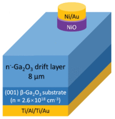
Figure 1: Schematic device structures of the vertical NiO/β-Ga₂O₃ heterojunction p-n diode fabricated on a bulk β-Ga₂O₃ substrate.[12]
This heterojunction diode exhibited an ultra-high breakdown voltage at 1059 V and an ultra-low reverse leakage current density of less than 1 μA/cm² before breakdown, demonstrating its extremely high application potential in power devices and precision rectifiers. Meanwhile, it also showed a relatively low Ron,sp at approximately 3.5 mΩ·cm², implying its ideal high-power handling capacity and providing a solution for system miniaturization and the enhancement of system reliability. And the capacitance values exhibited by this heterojunction diode at 100 kHz and 1 MHz were almost identical, which meaned it possessed excellent junction capacitance characteristics and showed high-frequency adaptability as well as broadband application capabilities. Figure 2 shows some electrical characteristics of the heterojunction diode.
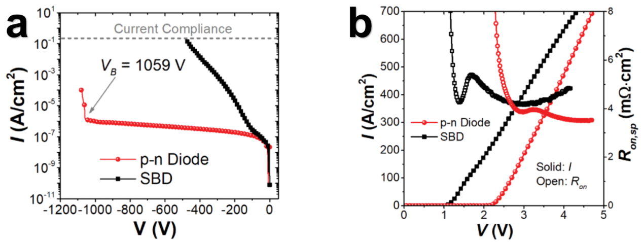
Figure 2: I-V curve of the breakdown characteristics of the heterojunction (a), the volt-ampere characteristics of the heterojunction (b).[12]
However, the report indicated that when the diode operated within 125 °C, the ideality factor was approximately in the range of 1.22 to 1.57, implying the exsistence of the interface recombination mechanism during the conduction process of the device. Regarding this, there might be negative impacts such as higher power consumption, thermal dissipation, and trouble on high-frequency switch. Thus, subsequent optimization research is in need. Since defects may exist at the NiO/β-Ga₂O₃ interface, it is necessary to further improve the interface quality, such as optimizing the heterojunction growth process or passivation treatment on the interface. There was study pointing out that annealing the HJD in air at 300 °C for one hour can effectively reduce the interface defects, revealing a promising prospect for high-performance p-NiO/n-Ga₂O₃ heterojunctions[13].
3.3. p-GaN/n-Ga2O3 heterojunction
The p-GaN/n-Ga₂O₃ heterojunction diode is widely utilized in the optoelectronic field due to its outstanding self-powered characteristics and sensitive ultraviolet response[5]. But its application in the direction of power devices still is worthy of attention. Power devices are more sensitive to interface effects compared with optoelectronic devices. Nevertheless, as GaN and Ga₂O₃ have different crystal structures and lattice parameter mismatches, the interface generated by directly bonding the two materials would lead to excessive defects. Therefore, when constructing power devices, it is necessary to conduct a transition layer. ZnO had been proved to be a choice for combine GaN and Ga₂O₃ as a transition layer. Jian et. al. has reported the construction of p-GaN/n-Ga₂O₃ heterojunction diode[14]. Firstly, the 5×5 mm² GaN substrate and the 10×10 mm² Ga₂O₃ substrate were ultrasonically cleaned in acetone, isopropyl alcohol and deionized water, and then soaked in buffered hydrofluoric acid (BHF) for 30 seconds. Subsequently, the samples were immediately placed into an atomic layer deposition (ALD) chamber to minimize any surface contamination. At 200 °C, using diethylzinc (DEZ) and water as precursors, a 10-nm-thick ZnO layer was deposited on the N-polar GaN and (-201) Ga₂O₃ samples by thermal ALD. Then, the GaN sample was flipped onto the Ga₂O₃ sample and transferred into an EVG 510 bonding chamber. In a vacuum, the samples were bonded at a pressure of 4 MPa and a temperature of 550 °C for 3 hours. Figure 3 illustrates the fabrication process of the heterojunction with this special structure.
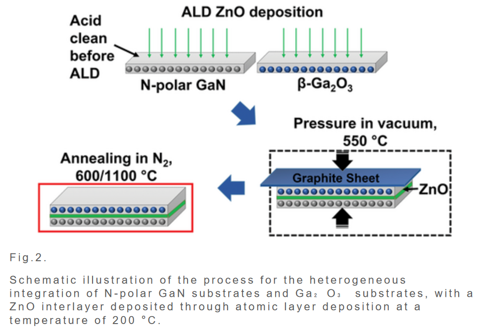
Figure 3: Schematic illustration of the process for the heterogeneous integration of N-polar GaN substrates and Ga2O3 substrates, with a ZnO interlayer deposited through atomic layer deposition at a temperature of 200 °C [14].
This method had successfully fabricated a heterojunction exhibiting excellent diode I-V characteristics and exhibited a relatively low Ron, which implies that there are fewer interface defects and the energy band bends normally. Moreover, the sample demonstrated a high bonding strength. Consequently, this heterojunction may possess a greater mechanical strength benefiting from the extremely high hardness of the both materials, ensuring its structural stability. However, the thermal stability of this device might not be that satisfactory. By comparing the operating curves at 300K from the original devices and devices after 650K treatment, obvious ohmic behavior in electrical characteristics of the heat-treated device was observed. The results showed the limitation of the high-temperature usage of the GaN/Ga2O3 device. On the other hand, the GaN/Ga2O3 device exhibited a relatively low rectification ratio, which implies that it may not meet the requirements in precision instruments. Additionally, some studies have pointed out that compared with the zero-bias condition, the photoresponse time of this heterojunction is longer under forward bias, which indicated that there are trap states at the interface with non-negligible impact. Subsequently, in terms of power devices, the GaN/Ga2O3 heterojunction may be not as outstanding as it is in the field of optoelectronic devices. Further research on improving the GaN/Ga2O3 interface may be the key to unlocking the full potential of the p-GaN/n-Ga2O3 heterojunction. Figure 4 shows some electrical characteristics of the heterojunction diode.
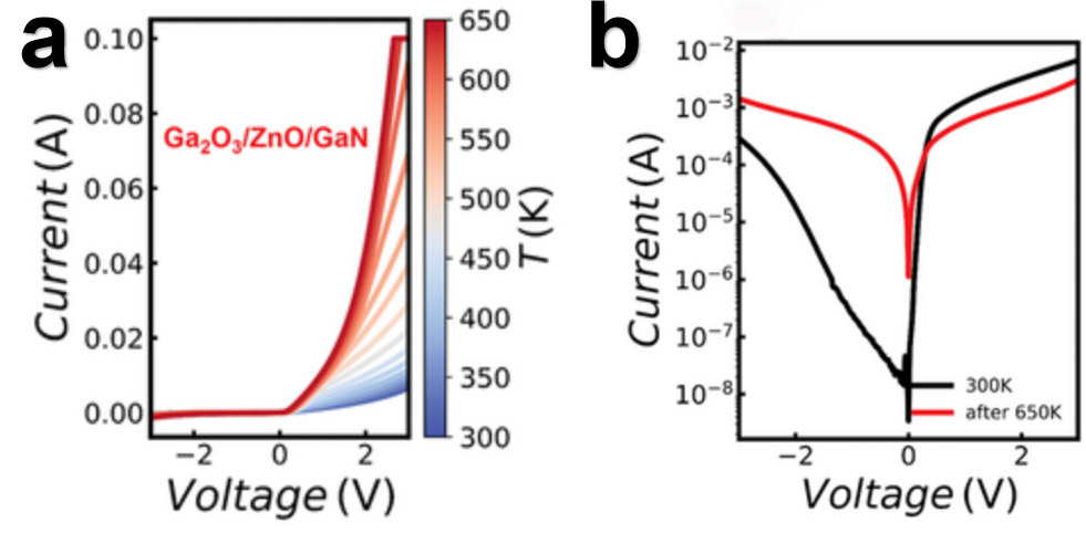
Figure 4: a) The volt-ampere characteristics of the heterojunction. b) I–V characteristics in semi-log scale taken at 300 K before and after temperature-dependent measurement.[14]
3.4. p-diamond/n-Ga2O3 heterojunction
Among numerous wide bandgap materials, single-crystalline p-type diamond possesses the highest electron and hole mobilities as well as the highest Baliga's figure of merit. Due to the differences in thermal expansion coefficients and lattice mismatches, the traditional method of directly growing one material on top of the other may not be applicable. Low-temperature growth methods might be the ideal approach[15]. For example, a low-temperature thermal dehydration direct bonding method was reported as follows: At 75 °C, the diamond substrate was OH-terminated using an H₂O₂/NH₄OH/H₂O (1:1:5) mixture for 10 minutes. Meanwhile, the surface of β-Ga₂O₃ was irradiated with oxygen plasma for 30 seconds at 200 W and 60 Pa using the reactive ion etching (RIE) technique. By this method, the root mean square (rms) roughness of the β-Ga₂O₃ and diamond surfaces was 0.33 nm and 0.12 nm respectively. Under atmospheric conditions, the surfaces of diamond and β-Ga₂O₃ were brought into contact with each other. After being stored with a desiccant for 72 hours, the samples were annealed at 250 °C for 24 hours to obtain a heterojunction with a more favorable interface. Figure 5 illustrates this production process.
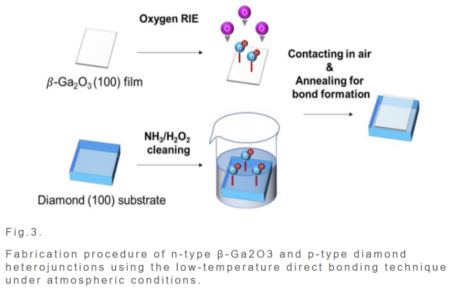
Figure 5: Fabrication procedure of n-type β-Ga₂O₃ and p-type diamond heterojunctions using the low-temperature direct bonding technique under atmospheric conditions.[15]
This heterojunction diode exhibited a high rectification ratio greater than 1x10⁸, demonstrating its broad prospects in power rectification. Moreover, thanks to the extremely high thermal conductivity of diamond, this product may possess better high-power adaptability in high heat dissipation needed situation. However, the C²-V relationship of this heterojunction deviated from linearity, which may be due to the inhomogeneity during the p-doping of diamond. This may lead to severe signal distortion in high-frequency applications. Meanwhile, the relatively small ideality factor indicateed that although there are no significant defects at the junction interface, it still shows a relatively high turn-on voltage (Von) of 4.5 V. This may be related to the energy band of the two materials. The high Von substantially increased the power consumption and caused heat dissipation issues. Though the high thermal conductivity of diamond might ease the defect, further research by menas of energy band engineering may be required in the future to enable the normal bending of the energy band and thus to enhance its performance.Figure 6 shows some electrical characteristics of the heterojunction diode.
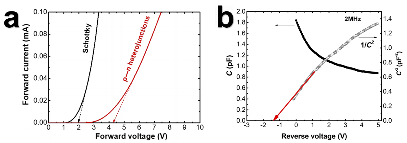
Figure 6: a) Forward volt-ampere characteristics of the heterojunction. b) capacitance-voltage characteristics of the p-n heterojunction [16].
4. Comparison & Suggestion
Based on the above, Table 1 compares the performances of different β-Ga₂O₃ devices.
Table 1: Comparison of different β-Ga₂O₃ devices.
Type | Advantages | Disadvantages |
Elements doped homojunction | -No interface effect -Higher theoretical performance | -Hard for effective doping -Hard to mass production |
NiO heterojunction | -High breakdown voltage -Low leakage current -Excellent high - frequency adaptability | -Interface defects impact |
GaN heterojunction | -High mechanical strength, -Less interface defects | -Narrow operating temperature range, -Complicated manufacturing process, -Low rectification ratio |
Diamond heterojunction | -Large rectification ratio, -Robust heat - dissipation capability | -Hard for uniform doping uniformly, -High Ron |
As can be seen from the comparison shown in Table 1, different implementation schemes of Ga₂O₃ power devices possess distinct characteristics and thus have different application scopes. From a long-term and scientific perspective, doping β-Ga₂O₃ to form a homojunction is surely the ultimate approach to exploit its excellent properties, as it eliminates the defects generated at the interface during the combination of two materials. From the perspective of current and industrial production, forming a heterojunction is an effective way to achieve a high-performance pn junction. Among them, in terms of power devices, the heterojunction with NiO as the p-type material exhibits the most outstanding electrical characteristics and is highly suitable for high-power and high-frequency application scenarios. The extremely low leakage current enables application of p-NiO/n-Ga₂O₃ in precision electronic equipment. However, the interface effect may cause waste heat during its operation, which means that it requires the cooperation with heat dissipation technology to operate at high power and thus may have a good application prospect in large power equipment equipped with special heat dissipation devices. The p-GaN/n-Ga₂O₃ heterojunction has already shown a leading edge in the field of optoelectronic. Its high bonding strength implies that it may be applicable to scenarios with strict requirements for mechanical strength such as the military and aerospace fields. However, its cumbersome production process may limit its further application in consumer-grade power devices. Benefiting from the strong heat dissipation ability and high rectification ratio, the p-diamond/n-Ga₂O₃ heterojunction may be suitable for miniaturized and portable information processing devices, such as smart phones. But its poor frequency characteristics due to the difficulty in uniform doping mean that it may not meet the requirements of wideband applications. The different characteristics of different schemes provide corresponding solutions for Ga₂O₃ in various scenarios, fully demonstrating its application potential, and also offering rich technical paths for researchers in the research and development of semiconductor devices.
5. Conclusion
In the field of power devices, the research on β-Ga₂O₃ heterojunctions is of great significance. Through the discussion of different implementation schemes of β-Ga₂O₃ power devices, each scheme has unique characteristics and application scenarios. The element-doped homojunction has the advantages of no interface effect, etc., but currently faces the difficulties in conducting effective p-type doping and inability to mass-produce. However, from a long-term and scientific perspective, it may still be the ultimate way to exploit the excellent properties of β-Ga₂O₃. The p-NiO/n-Ga₂O₃ heterojunction exhibits excellent performance as power devices with high breakdown voltage, low leakage current, and excellent high-frequency adaptability. However, the interface defects have an negative impact on its performance. Future efforts should focus on improving the interface quality to further enhance its performance, and it is expected to play an important role in large power equipment. The p-GaN/n-Ga₂O₃ heterojunction has obvious advantages in the optoelectronic field, but there are problems such as narrow operating temperature range, complex manufacturing process, and low rectification ratio in power device applications. Subsequent improvement of its interface characteristics will be the key to unlocking its potential in the power device field. The p-diamond/n- Ga₂O₃ heterojunction, with its high rectification ratio and strong heat dissipation ability, is suitable for miniaturized information processing devices. However, the difficulty in uniform doping of diamond leads to poor frequency characteristics, and future efforts need to be made to improve its performance through means such as energy band engineering. The research investigated diverse choices for Ga₂O₃ in various application scenarios, fully demonstrating the application potential and flexibility of the material, and also providing rich technical ideas for researchers in the research and development of semiconductor devices, which helps to promote the relevant industries to move towards a more refined and diversified direction.
References
[1]. Playford, H. Y., Hannon, A. C., Barney, E. R., & Walton, R. I. (2013). Structures of Uncharacterised Polymorphs of Gallium Oxide from Total Neutron Diffraction. Chemistry – A European Journal, 19(8), 2803-2813. https://doi.org/https://doi.org/10.1002/chem.201203359
[2]. Higashiwaki, M., Sasaki, K., Kuramata, A., Masui, T., & Yamakoshi, S. (2012). Gallium oxide (Ga2O3) metal-semiconductor field-effect transistors on single-crystal β-Ga2O3 (010) substrates. Applied Physics Letters, 100(1). https://doi.org/10.1063/1.3674287
[3]. Cai, X., Sabino, F. P., Janotti, A., & Wei, S.-H. (2021). Approach to achieving a p-type transparent conducting oxide: Doping of bismuth-alloyed Ga₂O₃ with a strongly correlated band edge state. Physical Review B, 103(11), 115205. https://doi.org/10.1103/PhysRevB.103.115205
[4]. Zhou, X., Liu, Q., Hao, W., Xu, G., & Long, S. (2022, 22-25 May 2022). Normally-off β-Ga2O3 Power Heterojunction Field-Effect-Transistor Realized by p-NiO and Recessed-Gate. 2022 IEEE 34th International Symposium on Power Semiconductor Devices and ICs (ISPSD),
[5]. Li, P., Shi, H., Chen, K., Guo, D., Cui, W., Zhi, Y., Wang, S., Wu, Z., Chen, Z., & Tang, W. (2017). Construction of GaN/Ga2O3 p–n junction for an extremely high responsivity self-powered UV photodetector [10.1039/C7TC03746E]. Journal of Materials Chemistry C, 5(40), 10562-10570. https://doi.org/10.1039/C7TC03746E
[6]. Ma, C., Wu, Z., Jiang, Z., Chen, Y., Ruan, W., Zhang, H., Zhu, H., Zhang, G., Kang, J., Zhang, T.-Y., Chu, J., & Fang, Z. (2022). Exploring the feasibility and conduction mechanisms of P-type nitrogen-doped β-Ga2O3 with high hole mobility. Journal of Materials Chemistry C, 10(17), 6673-6681. https://doi.org/10.1039/D1TC05324H
[7]. Ebrahimi-Darkhaneh, H., Shekarnoush, M., Arellano-Jimenez, J., Rodriguez, R., Colombo, L., Quevedo-Lopez, M., & Banerjee, S. K. (2022). High-quality Mg-doped p-type Ga2O3 crystalline thin film by pulsed laser. Journal of Materials Science: Materials in Electronics, 33(31), 24244-24259. https://doi.org/10.1007/s10854-022-09146-0
[8]. Katayama-Yoshida, H., & Yamamoto, T. (1997). Materials Design of the Codoping for the Fabrication of Low-Resistivity p-Type ZnSe and GaN by ab-initio Electronic Structure Calculation. physica status solidi (b), 202(2), 763-773. https://doi.org/https://doi.org/10.1002/1521-3951(199708)202:2<763::AID-PSSB763>3.0.CO;2-C
[9]. Zhang, L., Yan, J., Zhang, Y., Li, T., & Ding, X. (2012). A comparison of electronic structure and optical properties between N-doped β-Ga2O3 and N–Zn co-doped β-Ga2O3. Physica B: Condensed Matter, 407(8), 1227-1231. https://doi.org/https://doi.org/10.1016/j.physb.2012.01.107
[10]. Joshi, U. S., Matsumoto, Y., Itaka, K., Sumiya, M., & Koinuma, H. (2006). Combinatorial synthesis of Li-doped NiO thin films and their transparent conducting properties. Applied Surface Science, 252(7), 2524-2528. https://doi.org/https://doi.org/10.1016/j.apsusc.2005.03.239
[11]. Deng, Y., Yang, Z., Xu, T., Jiang, H., Ng, K. W., Liao, C., Su, D., Pei, Y., Chen, Z., Wang, G., & Lu, X. (2023). Band alignment and electrical properties of NiO/β-Ga2O3 heterojunctions with different β-Ga2O3 orientations. Applied Surface Science, 622, 156917. https://doi.org/https://doi.org/10.1016/j.apsusc.2023.156917
[12]. Lu, X., Zhou, X., Jiang, H., Ng, K. W., Chen, Z., Pei, Y., Lau, K. M., & Wang, G. (2020). 1-kV Sputtered p-NiO/n-Ga2O3 Heterojunction Diodes With an Ultra-Low Leakage Current Below 1μA/cm2. IEEE Electron Device Letters, 41(3), 449-452. https://doi.org/10.1109/LED.2020.2967418
[13]. Gong, H., Yu, X., Xu, Y., Zhou, J., Ren, F., Gu, S., Zhang, R., & Ye, J. (2021, 8-11 April 2021). Vertical Field-Plated NiO/Ga2O3 Heterojunction Power Diodes. 2021 5th IEEE Electron Devices Technology & Manufacturing Conference (EDTM),
[14]. Jian, Z., Sun, K., Kosanovic, S., Clymore, C. J., Mishra, U., & Ahmadi, E. (2023). Electrical and Structural Analysis of β-Ga2O3/GaN Wafer-Bonded Heterojunctions with a ZnO Interlayer. Advanced Electronic Materials, 9(8), 2300174. https://doi.org/https://doi.org/10.1002/aelm.202300174
[15]. Sittimart, P., Ohmagari, S., Matsumae, T., Umezawa, H., & Yoshitake, T. (2021). Diamond/β-Ga2O3 pn heterojunction diodes fabricated by low-temperature direct-bonding. AIP Advances, 11(10). https://doi.org/10.1063/5.0062531
Cite this article
Pang,Y. (2025). β-Ga2O3 Heterojunctions for Power Devices: A Review. Applied and Computational Engineering,117,220-229.
Data availability
The datasets used and/or analyzed during the current study will be available from the authors upon reasonable request.
Disclaimer/Publisher's Note
The statements, opinions and data contained in all publications are solely those of the individual author(s) and contributor(s) and not of EWA Publishing and/or the editor(s). EWA Publishing and/or the editor(s) disclaim responsibility for any injury to people or property resulting from any ideas, methods, instructions or products referred to in the content.
About volume
Volume title: Proceedings of the 3rd International Conference on Mechatronics and Smart Systems
© 2024 by the author(s). Licensee EWA Publishing, Oxford, UK. This article is an open access article distributed under the terms and
conditions of the Creative Commons Attribution (CC BY) license. Authors who
publish this series agree to the following terms:
1. Authors retain copyright and grant the series right of first publication with the work simultaneously licensed under a Creative Commons
Attribution License that allows others to share the work with an acknowledgment of the work's authorship and initial publication in this
series.
2. Authors are able to enter into separate, additional contractual arrangements for the non-exclusive distribution of the series's published
version of the work (e.g., post it to an institutional repository or publish it in a book), with an acknowledgment of its initial
publication in this series.
3. Authors are permitted and encouraged to post their work online (e.g., in institutional repositories or on their website) prior to and
during the submission process, as it can lead to productive exchanges, as well as earlier and greater citation of published work (See
Open access policy for details).
References
[1]. Playford, H. Y., Hannon, A. C., Barney, E. R., & Walton, R. I. (2013). Structures of Uncharacterised Polymorphs of Gallium Oxide from Total Neutron Diffraction. Chemistry – A European Journal, 19(8), 2803-2813. https://doi.org/https://doi.org/10.1002/chem.201203359
[2]. Higashiwaki, M., Sasaki, K., Kuramata, A., Masui, T., & Yamakoshi, S. (2012). Gallium oxide (Ga2O3) metal-semiconductor field-effect transistors on single-crystal β-Ga2O3 (010) substrates. Applied Physics Letters, 100(1). https://doi.org/10.1063/1.3674287
[3]. Cai, X., Sabino, F. P., Janotti, A., & Wei, S.-H. (2021). Approach to achieving a p-type transparent conducting oxide: Doping of bismuth-alloyed Ga₂O₃ with a strongly correlated band edge state. Physical Review B, 103(11), 115205. https://doi.org/10.1103/PhysRevB.103.115205
[4]. Zhou, X., Liu, Q., Hao, W., Xu, G., & Long, S. (2022, 22-25 May 2022). Normally-off β-Ga2O3 Power Heterojunction Field-Effect-Transistor Realized by p-NiO and Recessed-Gate. 2022 IEEE 34th International Symposium on Power Semiconductor Devices and ICs (ISPSD),
[5]. Li, P., Shi, H., Chen, K., Guo, D., Cui, W., Zhi, Y., Wang, S., Wu, Z., Chen, Z., & Tang, W. (2017). Construction of GaN/Ga2O3 p–n junction for an extremely high responsivity self-powered UV photodetector [10.1039/C7TC03746E]. Journal of Materials Chemistry C, 5(40), 10562-10570. https://doi.org/10.1039/C7TC03746E
[6]. Ma, C., Wu, Z., Jiang, Z., Chen, Y., Ruan, W., Zhang, H., Zhu, H., Zhang, G., Kang, J., Zhang, T.-Y., Chu, J., & Fang, Z. (2022). Exploring the feasibility and conduction mechanisms of P-type nitrogen-doped β-Ga2O3 with high hole mobility. Journal of Materials Chemistry C, 10(17), 6673-6681. https://doi.org/10.1039/D1TC05324H
[7]. Ebrahimi-Darkhaneh, H., Shekarnoush, M., Arellano-Jimenez, J., Rodriguez, R., Colombo, L., Quevedo-Lopez, M., & Banerjee, S. K. (2022). High-quality Mg-doped p-type Ga2O3 crystalline thin film by pulsed laser. Journal of Materials Science: Materials in Electronics, 33(31), 24244-24259. https://doi.org/10.1007/s10854-022-09146-0
[8]. Katayama-Yoshida, H., & Yamamoto, T. (1997). Materials Design of the Codoping for the Fabrication of Low-Resistivity p-Type ZnSe and GaN by ab-initio Electronic Structure Calculation. physica status solidi (b), 202(2), 763-773. https://doi.org/https://doi.org/10.1002/1521-3951(199708)202:2<763::AID-PSSB763>3.0.CO;2-C
[9]. Zhang, L., Yan, J., Zhang, Y., Li, T., & Ding, X. (2012). A comparison of electronic structure and optical properties between N-doped β-Ga2O3 and N–Zn co-doped β-Ga2O3. Physica B: Condensed Matter, 407(8), 1227-1231. https://doi.org/https://doi.org/10.1016/j.physb.2012.01.107
[10]. Joshi, U. S., Matsumoto, Y., Itaka, K., Sumiya, M., & Koinuma, H. (2006). Combinatorial synthesis of Li-doped NiO thin films and their transparent conducting properties. Applied Surface Science, 252(7), 2524-2528. https://doi.org/https://doi.org/10.1016/j.apsusc.2005.03.239
[11]. Deng, Y., Yang, Z., Xu, T., Jiang, H., Ng, K. W., Liao, C., Su, D., Pei, Y., Chen, Z., Wang, G., & Lu, X. (2023). Band alignment and electrical properties of NiO/β-Ga2O3 heterojunctions with different β-Ga2O3 orientations. Applied Surface Science, 622, 156917. https://doi.org/https://doi.org/10.1016/j.apsusc.2023.156917
[12]. Lu, X., Zhou, X., Jiang, H., Ng, K. W., Chen, Z., Pei, Y., Lau, K. M., & Wang, G. (2020). 1-kV Sputtered p-NiO/n-Ga2O3 Heterojunction Diodes With an Ultra-Low Leakage Current Below 1μA/cm2. IEEE Electron Device Letters, 41(3), 449-452. https://doi.org/10.1109/LED.2020.2967418
[13]. Gong, H., Yu, X., Xu, Y., Zhou, J., Ren, F., Gu, S., Zhang, R., & Ye, J. (2021, 8-11 April 2021). Vertical Field-Plated NiO/Ga2O3 Heterojunction Power Diodes. 2021 5th IEEE Electron Devices Technology & Manufacturing Conference (EDTM),
[14]. Jian, Z., Sun, K., Kosanovic, S., Clymore, C. J., Mishra, U., & Ahmadi, E. (2023). Electrical and Structural Analysis of β-Ga2O3/GaN Wafer-Bonded Heterojunctions with a ZnO Interlayer. Advanced Electronic Materials, 9(8), 2300174. https://doi.org/https://doi.org/10.1002/aelm.202300174
[15]. Sittimart, P., Ohmagari, S., Matsumae, T., Umezawa, H., & Yoshitake, T. (2021). Diamond/β-Ga2O3 pn heterojunction diodes fabricated by low-temperature direct-bonding. AIP Advances, 11(10). https://doi.org/10.1063/5.0062531