


1. Introduction
The pursuit of renewable energy sources has become a global imperative as the world grapples with the issues of the depletion of fossil fuels and deterioration of environmental problems. Among various renewable energy technologies, solar energy stands out due to its abundance and sustainability. The development of compound solar cells has gained significant traction in recent years, primarily due to their potential for high efficiency and cost-effectiveness. Many candidates have been studied for decades, but some intrinsic defects limit their applications. For example, though CdTe solar cells are known for their relatively high efficiency and commercial viability, the toxicity of cadmium and the scarcity of tellurium pose significant environmental and economic concerns, limiting their large-scale deployment [1]. Cu-In-Ga-Se (CIGS) solar cells offer excellent performance and flexibility in tuning the bandgap. Nevertheless, the high cost and limited availability of indium and gallium, along with the complexity of the fabrication process, remain major obstacles [2]. Perovskite solar cells have attracted interest because they are highly efficient and cost-effective, but issues related to long-term reliability and lead toxicity continue to challenge their practical application [3]. Antimony selenide (Sb2Se3) has emerged as a promising material for next-generation compound solar cells, owing to its excellent photovoltaic properties and abundant raw material availability [3].
The unique characteristics of Sb2Se3, including its suitable bandgap, high absorption coefficient, and benign environmental impact, make it attractive in solar cell research. In the last ten years, considerable advancements have been achieved in the development and optimization of solar cells based on Sb2Se3. Researchers have explored a variety of deposition techniques to fabricate high-quality Sb2Se3 thin films, aiming to achieve higher power conversion efficiencies (PCE) and better device stability [4]. Also, owing to its stability of the orthorhombic crystallographic phase, Sb2Se3 can withstand severe damp heat, and can endure prolonged exposure to moisture and light [1]. The unique quasi-1D structure endows Sb2Se3 with anisotropic optical and electrical properties, which make it worthy for research [3].
Despite these advantages, Sb2Se3 faces a critical challenge in attaining high power conversion efficiency (PCE). The current record for planar Sb2Se3 thin-film solar cells is a modest 8.64%, significantly lagging behind the efficiency of traditional silicon solar cells [5]. One of the main reasons of such efficiency is the grain size limitations by the current deposition techniques. The grain size measured in the recent researches are only about hundreds of nanometers, much smaller than the film thickness [1]. Additionally, a high concentration of deep defects in the bulk Sb2Se3 leads to a reduced open circuit voltage (Voc) and fill factor (FF) [3]. Several strategies are being pursued to enhance the efficiency of Sb2Se3 solar cells, including optimizing crystal vertical alignment growth by orientation controlling, and innovating deposition techniques.
In this article, preparation methods of Sb2Se3 thin film that had been explored in the past decades were compared. The main content of this review is organized into three sections. The first section is the case study of two predominant (physical/chemical) preparation schemes, among which 6 film preparation methods are selected to evaluate from there light efficiency, film forming efficiency, large-scale production possibility and future potential. The second section provides an in-depth analysis of these methods, highlighting their respective strengths and weaknesses. The final section introduces our proposed solutions of increasing the efficiency of Sb2Se3 solar cells, offering a roadmap for future enhancements in this promising field.
2. Design & Fabrication method
The fabrication of Sb2Se3 solar cells film could be roughly divided into two parts: physical & chemical methods, for physical methods, Thermal Evaporation, Vapor Transport Deposition (VDT), Electron-Beam Gun (EBG) deposition could be listed. For chemical methods, there are Spin Coating (SC), Chemical Bath Deposition (CBD), and Hydrothermal synthesis under development.
2.1. Physical method
Thermal Evaporation. Thermal evaporation works by heating a solid material until it reaches its evaporation temperature and vaporizes in vacuum. The vapor then condenses on a cooler substrate, forming a thin film. The advantages of thermal evaporation include simple equipment, easy operation, and applicability to a variety of materials.
Vapor Transport Deposition. Vapor Transport Deposition is a method used to deposit thin films and grow crystals by transporting material in the vapor phase from a source to a substrate. Vapor Transport Deposition is advantageous for its ability to deposit materials with high precision and control over film thickness and composition.
Electron-Beam Gun deposition. Electron-Beam Gun Deposition, also known as Electron-Beam Physical Vapor Deposition (EBPVD), is a highly precise thin-film deposition technique used to create high-quality coatings. EBG deposition is valued for its precision and ability to produce high-purity films.
2.2. Chemical method
Spin coating. Spin coating is a generally operated on a cleaned silicon substrate. At first, an appropriate amount of liquid coating material is dispensed onto its center. The substrate is attached to a spin coater, which is a machine that spins the substrate at high speeds. The initial low speed helps spread the liquid, and then the speed is ramped up to the desired level. As the substrate spins, centrifugal forces push the liquid outward, causing it to spread. The speed of spinning and the duration determine the thickness of the film.
Chemical Bath Deposition. The fundamental setup for CBD consists of a container holding the deposition solution and a substrate where the film will be deposited. The procedure can be conducted either in an open or a closed system, with the closed system being more commonly used to avoid contamination. A soluble salt of the target metal is dissolved in water to release metal cations. A source compound for the non-metallic component is also included, which breaks down in the presence of hydroxide ions to produce non-metal anions. These anions and cations subsequently react to form the intended compound. The CBD deposition is governed by chemical reactions, which can be adjusted to yield uniform, well-adhered films that are consistently reproducible.
Hydrothermal synthesis. Hydrothermal synthesis is a technique involves utilizing a sealed pressure vessel for material preparation, then dissolving and then recrystallizing the material for powder formation Compared to other powder preparation methods, hydrothermal synthesis yields powders with well-developed grains, small and uniformly distributed particle sizes, and reduced particle agglomeration. Additionally, it allows for the use of more cost-effective raw materials and facilitates the attainment of the desired stoichiometry and crystal morphology.
Hydrothermal method for preparing nanostructures: it can synthesize nanomaterials at low temperatures, avoiding damage to the material structure at high temperatures; it has strong controllability, allowing precise manipulation on the shape and size of the materials; it has wide applicability, capable of preparing various types of nanomaterials; the purity of the synthesized materials is high, the operation is simple, and the cost is low, making it an environmentally friendly synthesis method.
3. Analysis & challenge
3.1. Thermal Evaporation
The thermal evaporation method was used to fabricate Sb₂Se₃ thin films by heating a mixture of Sb₂S₃ and Sb₂Se₃ powders in a vacuum chamber at 3 × 10⁻⁵ Torr. The substrate was preheated to 425°C, and the deposition rate was maintained at 10–15 nm/min. This controlled process ensured uniform thin films with a thickness range of 290–320 nm. Post-deposition, these films were combined with FTO and CdS layers to form a heterojunction solar cell structure. Graphite and silver paints were applied to form electrodes on the cell, with an active area of approximately 0.5 cm². The photos and the cross-sectional view were shown in figure 1. The fabrication process is simple and cost-effective, relying on widely available raw materials and equipment [6].
The solar cells demonstrated an average PCE of 5.6%, with the highest efficiency reaching 5.9% as shown in figure 2. Additional performance metrics included a Voc of 0.453 V, a Jsc of 24.7 mA/cm², and a FF of 0.53. Although the efficiency is modest compared to other techniques, thermal evaporation is attractive due to its scalability and cost-effectiveness. With further optimization of source materials and deposition parameters, this method could achieve higher efficiencies and become more viable for industrial-scale production [6].
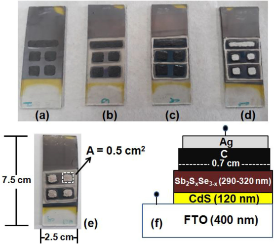
Figure 1: (a) Solar cell structure with hand-painted graphite electrodes of area; (b) solar cell delineated by etching-off boundary areas; (c) colloidal silver paint electrodes painted on the FTO-coating; (d) solar cells with colloidal graphite paint, thus finishing the cell structure; e) active cell area (A) of 0.5 cm2 and f) cross-sectional schematic of the solar cell [6].
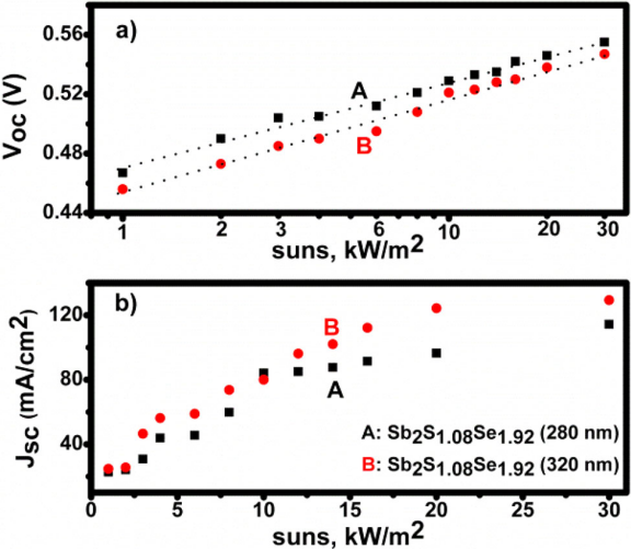
Figure 2: (a) Logarithmic increase of Voc of solar cells A and B with increase in intensity of illumination under the sun; (b) corresponding increase in Jsc [6].
3.2. Vapor Transport Deposition
VTD was employed to grow Sb2Se3 thin films with superior crystallinity and reduced defect density. The deposition process shown in Figure 3 was optimized to achieve a source temperature of 510°C, a substrate temperature of 390°C, and a chamber pressure of 3.2 Pa. These parameters enabled the growth of films with a predominant [221] crystallographic orientation, which is crucial for efficient charge transport and reduced recombination losses. The precise control over deposition parameters facilitated the fabrication of high-quality films, compatible with scalable and cost-effective production processes. VTD is similar to commercial CdTe photovoltaic fabrication processes makes it an appealing choice for industrial applications [7].
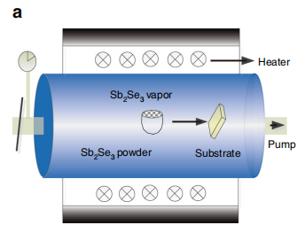
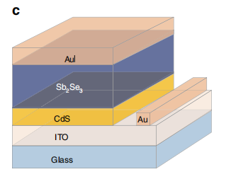
Figure 3: Fabrication of CdS/ Sb2Se3 solar cells. (a) Schematics of the VTD system. (b) Evolution of crystallinity with the optimization of deposition condition. (c) The device structure of the Sb2Se3 solar cells [7].
As shown in Figure 4, VTD-fabricated devices achieved a record PCE of 7.6%, surpassing previous efficiencies for Sb2Se3 thin-film solar cells. Performance metrics included a Voc of 0.42 V, a Jsc of 29.9 mA/cm², and an FF of 60.4%. The films exhibited lower recombination losses and improved carrier transport properties due to enhanced crystallinity and defect control. The results show that VDT is applicable for producing high-efficiency devices while maintaining scalability and cost-effectiveness. The technique’s compatibility with commercial manufacturing processes further solidifies its promise for future photovoltaic applications [7].
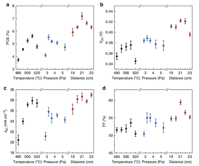
Figure 4: (a) Power conversion efficiency (PCE), (b) open-circuit voltage (Voc), (c) short-circuit current density (Jsc) and d fill factor (FF) of the CdS/ Sb2Se3 solar cells fabricated by VTD process [7].
3.3. Electron-Beam Gun Deposition
Electron-Beam Gun (EBG) deposition was used to fabricate Sb2Se3 thin films on Mo-coated glass substrates. The bulk Sb2Se3 material was synthesized using a mechano-chemical method and evaporated in a graphite crucible during deposition. The substrate temperature was maintained at 320°C to ensure uniform growth. After deposition, a reactive thermal annealing (ReTA) process was conducted at 350°C in a selenium-rich atmosphere. This post-deposition treatment improved the stoichiometry and crystalline quality of the films. The annealing process was performed under controlled conditions to ensure uniform grain growth and defect reduction, making the films more suitable for photovoltaic applications [8].
Table 1: Device characteristics of the Sb2Se3 solar cells fabricated using the films grown at the substrate temperature of 320 ℃ and annealed at various temperatures[8].
Annealing Temperature | Jsc(mA/cm2) | Voc(mV) | FF(%) | PCE(%) |
320°C | 21.9 | 317 | 51.4 | 4.2 |
350°C | 19.8 | 386 | 56.7 | 4.3 |
380°C | 18.5 | 294 | 47.3 | 2.6 |
As shown in Table 1, EBG-fabricated solar cells exhibited a PCE of approximately 4.34%, with significant improvements observed after annealing. The annealed films displayed enhanced stoichiometry and crystalline quality, which contributed to better photovoltaic performance. Although the PCE is lower compared to VTD-fabricated devices, the precise control over deposition and annealing conditions demonstrates EBG’s potential for further optimization. Future work could focus on refining annealing temperatures and environmental conditions to increase efficiency. This method is promising for achieving high-quality films in industrial applications [8].
3.4. Spin Coating
The preparation of uniform Sb2Se3 thin film can be achieved through the spin-coating technique via process in Figure 5. For instance, a typical Sb2Se3 synthesis method is described as follows: The Sb and Se powder (Te is not necessary) is added to a mixture of ethylenediamine (EA) and mercaptoethanol (ME) with a volume ratio of 4:1. After that, a stirring is processed about 4 hrs at 60℃ in order to obtain homogenous solution. Then the Sb-Se precursor solution is spun on fluorine-doped tin oxide (FTO), followed by a step of thermal decomposition [9].
Based on single-source precursor, the spin-coating method excels in the incorporation of additional elements into Sb2Se3 with high quality, thereby providing an outstanding platform for the exploration of defect characteristics and the optimization of efficiency. The Sb2Se3 thin films, doped with Te, have demonstrated a remarkable capacity to mitigate deep-level defects, such as hole traps The SEM images of the products is shown in Figure 6.
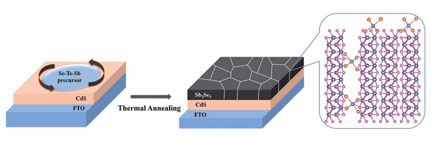
Figure 5: Schematic illustration of the Sb2Se3 film deposition and the atomic coordination in Sb2Se3 films [9].
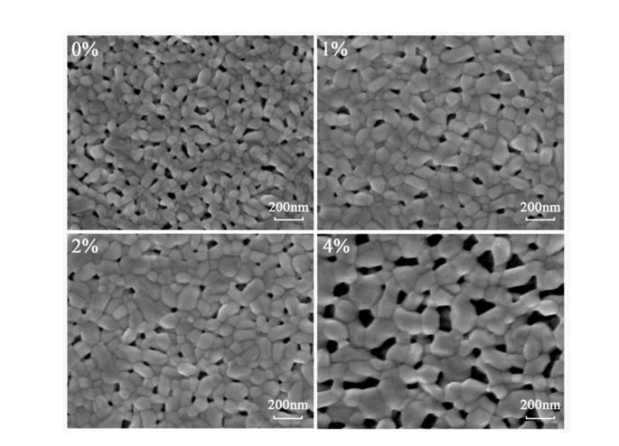
Figure 6: SEM images of the pristine Sb2Se3 film and Sb2Se3 with different Te doping concentrations [9].
However, although the spin-coating method is excellent in laboratory scale, its potential in mass production may be limited due to the need to deal with large-area substrates.
3.5. Chemical Bath Deposition
CBD has emerged as a successful technology capable of fabricating high-quality Sb2Se3 thin films that are well-suited for laboratory applications. A typical Sb2Se3 synthesis via CBD involves: introduction of SbCl3 into robust ligand such as sodium citrate solution in order to form soluble complexes with antimony, followed by the addition of ammonia and selenide precursor such as sodium selenosulfate with deionized water; The mixture is then subjected to a bath deposition process on a glass substrate at 50°C for 60 min [10].
The chemical reactions in CBD occur in solution under mild conditions, allowing for more accurate control over the reaction rate and the nucleation process. The reactants used in CBD are in ionic form instead of atomic, which contributes to the formation of a smoother and more uniform film morphology. The prepared thin film shows good coverage and consists of spindle-shape grains as shown in Figure 7. [10]. Compared to the vacuum method, which often necessitates the use of costly vacuum equipment, CBD presents itself as a cost-effective alternative for the large-scale fabrication of films.
However, almost all synthesis Sb2Se3 thin films are amorphous and require post-annealing, which introduce additional defects. Moreover, the careful selection of additives is crucial to prevent impurities in the final films. Furthermore, the disposal of residual products, which are classified as special waste, adds to the overall cost and raises environmental concerns.
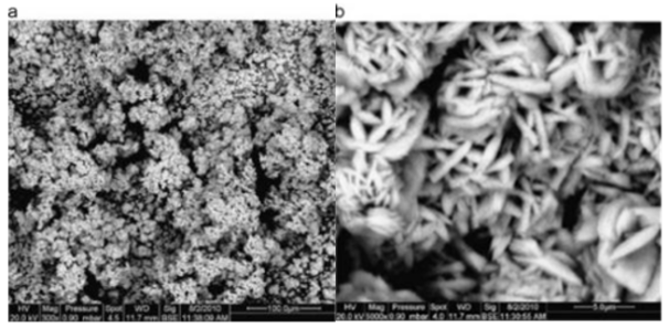
Figure 7: SEM images of Sb2Se3 thin film prepared by CBD at: (a) 300× and (b) 5000× magnifications [10].
3.6. Hydrothermal synthesis
Interface-enhanced Sb2Se3 solar cells comprising an ultrathin and uniform antimony selenide buffer layer via hydrothermal approach. [11], Zhou et. al. successfully prepared an ultra-thin and uniform Sb2Se3 buffer layer by hydrothermal method. The specific method is to adjust the molar ratio of Se to Na2SO3 in the selenium source to 1:6. Na2SeSO3 solution was prepared by hydrothermal reaction. Then, tartrate bismuthate and thiourea were dissolved in water, and Na2SeSO3 solution was added to form milky white solution. This solution and FTO/CdS substrate were placed at 100 °C for hydrothermal reaction for 60 minutes to form Sb2Se3 buffer layer as shown in Figure 8.
Sb2Se3 buffer layer prepared by hydrothermal method significantly improves the light efficiency and film-forming efficiency of GeSe solar cells. It is mentioned in the literature that the solar cell efficiency of Sb2Se3 buffer layer by hydrothermal method reaches 3.33 %. In addition, hydrothermal method is carried out at a lower temperature (135 °C), which means lower energy consumption and cost, which is beneficial to large-scale production.
There are also some challenges and limitations. Firstly, the reaction time of hydrothermal method is relatively long (60 minutes), which may limit the production efficiency, especially in large-scale production. Secondly, hydrothermal method requires precise control of reaction conditions, which may increase the complexity of the process. Therefore, although hydrothermal method performs well in laboratory scale, its feasibility in industrial scale application still needs further research and optimization.
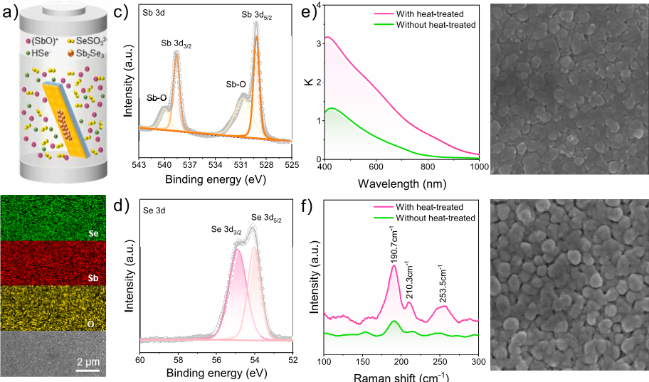
Figure 8: (a) Schematic of the Sb2Se3 buffer layer prepared by hydrothermal deposition. (b) SEM image and EDS elemental mapping of the Sb2Se3 buffer layer. XPS spectra for (c) Sd 3d and (d) Se 3d. (e) Extinction coefficient spectra and (f) Raman spectra of the Sb2Se3 buffer layer before and after heat treatment. SEM images of the Sb2Se3 buffer layer (g) before and (h) after heat treatment [11].
One-dimensional Sb2Se3 nanostructures, including nanowires and nanorods was also successfully synthesized by a template-free hydrothermal method. The synthesis process involves dissolving Sb(AcO)3 and Na2SeO3 in water, adding hydrazine hydrate, transferring to a high-pressure reaction kettle lined with polytetrafluoroethylene, and keeping it at 120°C for 24 hours. Sb2Se3 nanostructures were obtained after impurity removal (Figure 9) [12].
The prepared Sb2Se3 nanowires and nanorods showed higher initial hydrogen storage capacity than bismuth sulfide nanostructures in electrochemical measurement. Especially at room temperature, Sb2Se3 nanowires show a high capacity of 225mah/g. These results indicate that Sb2Se3 nanostructures have potential applications in hydrogen storage and high-energy batteries.
Although the research successfully obtained Sb2Se3 nanostructures, it still faces some challenges. For example, hydrothermal method usually requires specific reaction conditions and equipment, which may limit its feasibility in industrial scale application. In addition, the stability and long-term cycle performance of nanostructures are also important factors to be considered in practical applications. The researchers pointed out that the electrochemical hydrogen storage performance of Sb2Se3 nanostructures is sensitive to their size, which means that the precise control of the size in the synthesis process is the key to achieve the best performance. Therefore, future research needs to further optimize the synthesis conditions and explore the application of these nanostructures in practical energy storage devices.
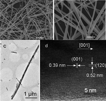
Figure 9: (a, b) Typical SEM images of as-prepared nanowires; (c) a part of an individual nanowire; and (d) corresponding HRTEM image of the individual nanowire [12].
4. Summary & suggestion
Table 2: comparison of various Sb2Se3 film preparing method.
method | Advantages | Disadvantages |
Thermal decomposition | -cost-effective -high-purity | -uneven for high T melt material -low efficient |
VTD | -effective in thin film -low process temperature | -high require for equipment |
EBG | -high precision and purity | -high require for equipment |
SC | -low cost -uniformity | -impurity |
CBD | -low cost -large scale -low temperature | -mostly amorphous -impurity |
Hydrothermal synthesis | -low temperature -cheap stuff -enable nanostructure | -time-consumption -environmental pollution -stability -size control |
The summary is concluded in Table 2., and advantages/disadvantages was proposed for each method. First, thermal evaporation is a cost-effective and straightforward thin-film deposition technique. It operates in a high vacuum, producing high-purity films with a wide range of material applicability, including metals and oxides. The process is quick, making it suitable for various applications requiring rapid deposition. On the other hand, thermal evaporation struggles with high melting point materials and may result in non-uniform film thickness over large substrates. Energy control is challenging compared to techniques like sputtering, potentially affecting film microstructure. Additionally, material utilization is often low, and environmental sensitivity can impact film quality.
VTD offers distinct advantages in thin film preparation, notably its ability to achieve large-area, uniform coatings suitable for metals, semiconductors, and organics. Operating at lower temperatures, it allows deposition on heat-sensitive substrates with precise control over film thickness and composition.
However, VTD demands high purity and flow control, often resulting in low material utilization and increased costs. While versatile, it requires complex optimization for high melting point or reactive materials. Despite its benefits in uniformity and scalability, the technique involves significant equipment and maintenance expenses.
EBG deposition is renowned for its high precision and purity in thin film deposition. It utilizes high energy to efficiently evaporate materials, resulting in uniform and pure films, which are ideal for applications in semiconductors and optical coatings. The technology is capable of handling high melting point materials and offers precise control over the film's thickness and composition, making it suitable for complex multilayer structures. Despite its advantages, EBG deposition comes with certain drawbacks. The equipment is costly and complex, requiring skilled operation and maintenance. The process must be conducted in a high vacuum environment, which increases operational costs and limits material choices. Additionally, the high energy of the electron beam can potentially damage certain substrates, restricting its use in some applications. These factors necessitate careful consideration when choosing EBG for specific projects.
SC allows for precise control over the thickness of the deposited film by changing the spin speed, which is crucial for optimizing the performance of solar cells. Moreover, it only dispense a thin layer of solution on the substrate, therefore consuming less solution and lower the cost. Since the process is conducted under non-vacuum conditions, impurities can be easily introduced into the film, which may affect the performance of the solar cell.
CBD of Sb2Se3 is generally operated below 100℃, which can reduce the cost of the process. Meanwhile, since it is simple to immerse substrate in the solution, this process can be applied in a large scale. However, the deposited thin films are mostly amorphous and need post- annealing. Also, the additives in the solution may introduce impurities.
Hydrothermal synthesis can be carried out at a lower temperature (135°C) and cheaper raw materials can be used, which means lower energy consumption and cost. However, the reaction time of hydrothermal synthesis method is relatively long (60 minutes), which may limit the production efficiency, and the treatment of residual products after synthesis is classified as special waste, which may cause environmental pollution.
Nano-structured Sb2Se3 shows higher performance than ordinary thin film, especially in photoelectric conversion efficiency and high initial hydrogen storage capacity. However, the stability and long-term cycle performance of nanostructures still need to be further improved. In addition, in order to achieve the best performance, the dimensions in the synthesis process need to be accurately controlled.
5. Conclusions
Sb2Se3 has proven to be a highly promising material for the next generation of thin-film solar cells, thanks to its abundance, non-toxic nature, and excellent photovoltaic properties. This review has explored various fabrication methods, including thermal evaporation, vapor transport deposition (VTD), electron-beam gun (EBG) deposition, spin coating (SC), chemical bath deposition (CBD), and hydrothermal synthesis. Each method comes with its own strengths: thermal evaporation is simple and cost-efficient, VTD enables the creation of high-quality films with precise crystal orientation, and EBG allows for highly accurate, multi-layered structures. On the other hand, chemical techniques like CBD and hydrothermal synthesis stand out for their low-temperature operations and scalability. However, issues such as defect formation, grain size limitations, and the extended reaction times of certain processes still need to be addressed. Despite these challenges, significant progress has been made. Achievements include reaching power conversion efficiencies of over 7.6% for VTD-fabricated Sb2Se3 cells and demonstrating improved light absorption and hydrogen storage with nanostructured devices. Yet, key obstacles remain, including high defect concentrations, suboptimal carrier lifetimes, and potential environmental concerns related to certain chemical methods. Looking ahead, improving crystal alignment and minimizing defect density through advanced deposition techniques will be crucial to further enhance device performance. The development of nanostructured Sb2Se3, particularly vertically aligned nanorod arrays, holds significant promise for better light absorption and carrier transport. Additionally, exploring novel doping strategies and new n-type materials could further optimize efficiency. Scaling up cost-effective and environmentally friendly manufacturing processes will also be critical to achieving broader adoption.
In conclusion, Sb2Se3-based solar cells offer a practical and sustainable path toward meeting global energy demands. Continued innovation in materials and manufacturing will ensure their future role in renewable energy solutions.
Authors Contribution
All the authors contributed equally, and their names were listed in alphabetical order.
References
[1]. Zhao, Q., Tang, R., Che, B., He, Y., Wu, T., & Peng, X. (2024). Grain‐Boundary Elimination via Liquid Medium Annealing toward High‐Efficiency Sb2Se3 Solar Cells. Advanced Materials. https://doi.org/10.1002/adma.202414082
[2]. Paul, R., Shukla, S., Lenka, T. R., Talukdar, F. A., & Nguyen, H. P. T. (2025). Design and performance analysis of novel perovskite/CZTSe hybrid solar cell for high efficiency. Solar Energy. https://doi.org/10.1016/j.solener.2024.113146
[3]. Chen, C., Li, K., & Tang, J. (2022). Ten Years of Sb2Se3 Thin Film Solar Cells. Solar RRL. https://doi.org/10.1002/solr.202200094
[4]. Duan, Z., Liang, X., Feng, Y., Ma, H., & Liang, B. (2022). Sb2Se3 Thin‐Film Solar Cells Exceeding 10% Power Conversion Efficiency Enabled by Injection Vapor Deposition Technology. Advanced Materials. https://doi.org/10.1002/adma.202202969
[5]. Tang, R., Chen, S., Zheng, Z.-H., Su, Z.-H., Luo, J.-T., Fan, P., Zhang, X.-H., Tang, J., & Liang, G.-X. (2022). Heterojunction Annealing Enabling Record Open-Circuit Voltage in Antimony Triselenide Solar Cells. Adv. Mater., 34, 2109078. https://doi.org/10.1002/adma.202109078
[6]. Ríos‐Ramirez, B., & Nair, P. K. (2018b). On the Stability of Operation of Antimony Sulfide Selenide Thin Film Solar Cells Under Solar Radiation. Physica Status Solidi (A), 215(24). https://doi.org/10.1002/pssa.201800479
[7]. Wen, X., Chen, C., Lu, S., Li, K., Kondrotas, R., Zhao, Y., Chen, W., Gao, L., Wang, C., Zhang, J., Niu, G., & Tang, J. (2018). Vapor transport deposition of antimony selenide thin film solar cells with 7.6% efficiency. Nature Communications, 9(1). https://doi.org/10.1038/s41467-018-04634-6
[8]. Tiwari, K. J., Neuschitzer, M., Espíndola-Rodriguez, M., Sánchez, Y., Jehl, Z., Vidal-Fuentes, P., Saucedo, E., & Malar, P. (2020). Efficient Sb2Se3/CdS planar heterojunction solar cells in substrate configuration with (hk0) oriented Sb2Se3 thin films. Solar Energy Materials and Solar Cells, 215, 110603. https://doi.org/10.1016/j.solmat.2020.110603
[9]. Ma, Y., Tang, B., Lian, W., Wu, C., Wang, X., Ju, H., Zhu, C., Fan, F., & Chen, T. (2020). Efficient defect passivation of Sb2Se3 film by tellurium doping for high performance solar cells. J. Mater. Chem. A, 8, 6510.https://doi.org/10.1039/D0TA00443J
[10]. Maghraoui-Meherzi, H., Ben Nasr, T., & Dachraoui, M. (2013). Synthesis, structure and optical properties of Sb2Se3. Materials Science in Semiconductor Processing, 16(1). https://doi.org/10.1016/j.mssp.2012.04.019
[11]. Zhou, J., Yang, S., Gao, L., Qu, Z., Cao, Y., Yu, X., Yu, X., Ni, J., & Zhang, J. (2024). Solar Energy Materials and Solar Cells. Advance online publication. Retrieved from https://doi.org/10.1016/j.solmat.2024.113260
[12]. Ma, J., Wang, Y., Wang, Y., Chen, Q., Lian, J., & Zheng, W. (2009). Controlled Synthesis of One-Dimensional Sb2Se3 Nanostructures and Their Electrochemical Properties. Journal of Physical Chemistry C, 113(31), 13588–13592. Advance online publication. Retrieved from https://doi.org/10.1021/jp902952k
Cite this article
Li,H.;Liu,J.;Wu,Z. (2025). Preparation Methods for Sb2Se3 Solar Films: Comparison and Evaluation. Applied and Computational Engineering,125,150-160.
Data availability
The datasets used and/or analyzed during the current study will be available from the authors upon reasonable request.
Disclaimer/Publisher's Note
The statements, opinions and data contained in all publications are solely those of the individual author(s) and contributor(s) and not of EWA Publishing and/or the editor(s). EWA Publishing and/or the editor(s) disclaim responsibility for any injury to people or property resulting from any ideas, methods, instructions or products referred to in the content.
About volume
Volume title: Proceedings of the 3rd International Conference on Mechatronics and Smart Systems
© 2024 by the author(s). Licensee EWA Publishing, Oxford, UK. This article is an open access article distributed under the terms and
conditions of the Creative Commons Attribution (CC BY) license. Authors who
publish this series agree to the following terms:
1. Authors retain copyright and grant the series right of first publication with the work simultaneously licensed under a Creative Commons
Attribution License that allows others to share the work with an acknowledgment of the work's authorship and initial publication in this
series.
2. Authors are able to enter into separate, additional contractual arrangements for the non-exclusive distribution of the series's published
version of the work (e.g., post it to an institutional repository or publish it in a book), with an acknowledgment of its initial
publication in this series.
3. Authors are permitted and encouraged to post their work online (e.g., in institutional repositories or on their website) prior to and
during the submission process, as it can lead to productive exchanges, as well as earlier and greater citation of published work (See
Open access policy for details).
References
[1]. Zhao, Q., Tang, R., Che, B., He, Y., Wu, T., & Peng, X. (2024). Grain‐Boundary Elimination via Liquid Medium Annealing toward High‐Efficiency Sb2Se3 Solar Cells. Advanced Materials. https://doi.org/10.1002/adma.202414082
[2]. Paul, R., Shukla, S., Lenka, T. R., Talukdar, F. A., & Nguyen, H. P. T. (2025). Design and performance analysis of novel perovskite/CZTSe hybrid solar cell for high efficiency. Solar Energy. https://doi.org/10.1016/j.solener.2024.113146
[3]. Chen, C., Li, K., & Tang, J. (2022). Ten Years of Sb2Se3 Thin Film Solar Cells. Solar RRL. https://doi.org/10.1002/solr.202200094
[4]. Duan, Z., Liang, X., Feng, Y., Ma, H., & Liang, B. (2022). Sb2Se3 Thin‐Film Solar Cells Exceeding 10% Power Conversion Efficiency Enabled by Injection Vapor Deposition Technology. Advanced Materials. https://doi.org/10.1002/adma.202202969
[5]. Tang, R., Chen, S., Zheng, Z.-H., Su, Z.-H., Luo, J.-T., Fan, P., Zhang, X.-H., Tang, J., & Liang, G.-X. (2022). Heterojunction Annealing Enabling Record Open-Circuit Voltage in Antimony Triselenide Solar Cells. Adv. Mater., 34, 2109078. https://doi.org/10.1002/adma.202109078
[6]. Ríos‐Ramirez, B., & Nair, P. K. (2018b). On the Stability of Operation of Antimony Sulfide Selenide Thin Film Solar Cells Under Solar Radiation. Physica Status Solidi (A), 215(24). https://doi.org/10.1002/pssa.201800479
[7]. Wen, X., Chen, C., Lu, S., Li, K., Kondrotas, R., Zhao, Y., Chen, W., Gao, L., Wang, C., Zhang, J., Niu, G., & Tang, J. (2018). Vapor transport deposition of antimony selenide thin film solar cells with 7.6% efficiency. Nature Communications, 9(1). https://doi.org/10.1038/s41467-018-04634-6
[8]. Tiwari, K. J., Neuschitzer, M., Espíndola-Rodriguez, M., Sánchez, Y., Jehl, Z., Vidal-Fuentes, P., Saucedo, E., & Malar, P. (2020). Efficient Sb2Se3/CdS planar heterojunction solar cells in substrate configuration with (hk0) oriented Sb2Se3 thin films. Solar Energy Materials and Solar Cells, 215, 110603. https://doi.org/10.1016/j.solmat.2020.110603
[9]. Ma, Y., Tang, B., Lian, W., Wu, C., Wang, X., Ju, H., Zhu, C., Fan, F., & Chen, T. (2020). Efficient defect passivation of Sb2Se3 film by tellurium doping for high performance solar cells. J. Mater. Chem. A, 8, 6510.https://doi.org/10.1039/D0TA00443J
[10]. Maghraoui-Meherzi, H., Ben Nasr, T., & Dachraoui, M. (2013). Synthesis, structure and optical properties of Sb2Se3. Materials Science in Semiconductor Processing, 16(1). https://doi.org/10.1016/j.mssp.2012.04.019
[11]. Zhou, J., Yang, S., Gao, L., Qu, Z., Cao, Y., Yu, X., Yu, X., Ni, J., & Zhang, J. (2024). Solar Energy Materials and Solar Cells. Advance online publication. Retrieved from https://doi.org/10.1016/j.solmat.2024.113260
[12]. Ma, J., Wang, Y., Wang, Y., Chen, Q., Lian, J., & Zheng, W. (2009). Controlled Synthesis of One-Dimensional Sb2Se3 Nanostructures and Their Electrochemical Properties. Journal of Physical Chemistry C, 113(31), 13588–13592. Advance online publication. Retrieved from https://doi.org/10.1021/jp902952k