


Review on the FPGA design optimization for ASIC
Xiaohaoyang Lei
School of Intelligent Engineering, Xi’an Jiaotong-liverpool University, SuZhou, JiangSu, 215123, China.
Xiaohaoyang.LEI20@student.xjtlu.edu.cn
Abstract. FPGA is a product of further development on programmable devices such as PAL and GAL. It is not only a chip, but a design pattern. With the rapid growth in FPGA performance and density, its complete top-down model can be applied to the development of similar ASICs while improving the technology itself. This paper shows that a summary analysis of previous articles can conclude that the application of FPGA design to ASICs can lead to optimization of many aspects. Architecture-level embedding and mapping transformation are the current mainstream application methods, both of which can bring strong economic and time benefits. Meanwhile, there are various issues that need special consideration in the application process which is related to the question of whether or not to map and convert. Finally, according to the analysis, we still need to solve two important issues which are the lack of automatic mapping tools and the lack of a unified function library in the future.
Keywords:FPGA, ASIC, VHDL, Hardware Description Language, Architecture Hierarchy Embedding.
1. Introduction
The FPGA device belongs to a kind of semi-custom circuit in an ASIC. It is a programmable logic array. Compared with the original device, it has more gate circuits. Compared with the traditional mode of chip design, FPGA chip and Design chips are not limited to research and development, but can be optimized by domain-specific products and designs, and optimized by specific chip models. Advanced CMOS process technologies (0.5–0.3 5 microns) and their architectures are changing the complexity and functionality of FPGA, with improved features being found for rapid prototyping of ASIC and improvements in power consumption and computation. In general design and use cases, ASIC and FPGA have advantages and disadvantages.The FPGA has extremely high reprogrammability, and the logic gate array can be modified anytime and anywhere. Using this feature can reduce the reconfiguration consumption of hardware. Another great advantage of FPGA is that, like ASIC, they can be designed and described using block diagrams or Verilog HDL. This greatly enhances the interoperability between them. But compared with ASIC, the ability of FPGA to perform arithmetic operations is not satisfactory [1], so it is a possible and feasible solution to use the design advantages of FPGA as the base plate to improve.
It is clear that there is no standard on how to apply FPGA design, but research and work basically revolve around architecture, description language, and front-end tools. At the architectural level, research more options to embed smaller FPGA units in ASIC systems to achieve improvement. This allows designers to set up algorithms in "reprogrammable" logic, and the embedded LiquidLogic Core (LL) architecture from LSI Logic, Milpitas, CA, provides the ability to modify data adjustment algorithms in real-time during immersive experiments [2].The co-design at the architectural level is similar to the semi-custom design scheme of ASIC. While completing the design requirements, it is flexible and can add or reduce functional units in time according to the requirements.
Thanks to the interoperability of VHDL, FPGA circuits may be mapped to other platforms, and a direct conversion can also be achieved. Most FPGA provide some pre-balanced, high-speed, low-skew routing lines. Therefore, these high-speed clock lines should be used more when designing ASIC in the same language in FPGA systems to improve prototype performance. Furthermore, a set of FPGA clock map buffers can be allowed to replace the ASIC clock tree in the prototype at the packaging stage [3].
This paper mainly introduces the research status of FPGA design system optimization of ASIC by means of review and qualitative analysis, and summarizes the relevant optimization methods. It is hoped that the optimization method can provide directional help for future research in the field of improvement directions.
2. Overview
2.1. ASIC
ASIC is divided into full-custom and semi-custom. Full custom design requires the designer to complete the design of all circuits, so it requires a lot of manpower and material resources. Although the flexibility is good, the development efficiency is low. If the design is ideal, a full custom can run faster than semi-custom ASIC chips. Semi-custom uses the standard logic cells in the library (Standard Cell), and can select SSI (gate circuit), MSI (such as adder, comparator), data path (such as ALU, memory, bus from the standard logic cell library during design), memory, and even system-level modules (such as multipliers, microcontrollers) and IP cores. Since these logic units have been laid out, and the design is more reliable, the designer can more easily complete the system design. Modern ASIC often contain an entire 32-bit processor, storage units like ROM, RAM, EEPROM, Flash, and other modules. Such ASIC are often referred to as SoC (systems on a chip).
2.2. FPGA
FPGA is the development branch of ASIC. Generally, the architecture system is modeled through block diagrams and VHDL, and EDA software is used to model, and simulate, and produce functional modules, which can be used after configuration to package templates. The biggest difference from ASIC is that it does not require users to participate in the arrangement of circuits and logic gates in the system. In addition, algorithms and circuit data can be adjusted in real time to achieve real-time modification and avoid resource waste. The semi-customized modular circuit is the biggest feature of FPGA. In experiments, this feature is used to improve the limitations of ASIC and to build the required architecture and design environment during mapping. Designers can no longer focus on the circuit diagram but must consider the placement of more modules to achieve greater area utilization.
3. Optimized path
3.1. Embedding at the architectural level
|
Figure 1. FPGA architecture for ASIC-FPGA co-design. |
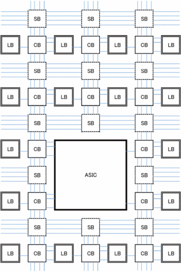
3.1.1. Hybrid architecture. The ASIC-FPGA co-design architecture is shown in Figure 1, which consists of the logic block LB in Figure 2.The switch block of Figure 3 , the connection block of Figure 4, and the ASIC block that realizes the main functions are constituted. LB is an FPGA composed of RTL design methods. Because of the use of RTL, the SB and CB of traditional FPGAs are developed using transistor switches, and their structure is different from Figure 3 and Figure 4 [5].
|
Figure 2. Structure of the lb. |
|
Figure 3. Structure of the sb. |
|
Figure 4. Structure of the cb. |
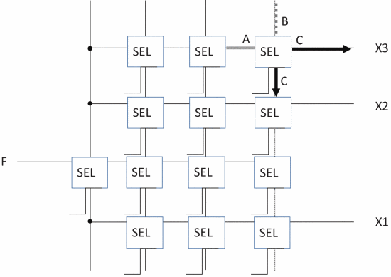
CB increases the connection between ASIC and FPGA. This makes the architecture easier to quickly replace circuits composed of LB with ASIC. Adding a CB expands the connection, and from an area perspective, reducing the CB allows the LB to go directly to the ASIC.
3.1.2. LL kernel architecture. The LL (Liquid Logic) kernel architecture has the same design idea but is reflected in the architecture. LL cores are provided by LSI according to customer specifications. The LL architecture consists of a GDS2 hard macro containing a multiscale array (MSA) and a soft gate-level core. One to sixteen hex blocks and an I/O wrapper make up the MSA (providing the ATPG scan function and the ASIC buffered acceptance of PLC signals). The soft core acts as a programming interface, and the programmable interface is driven by serial EEPROM and/or AMBA AHB bus interfaces.
|
Figure 5. MSA Architecture. |
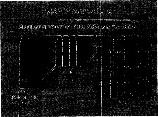
Figure 5 shows the internal structure of MSA. It can be seen that it is composed of multiple large arrays and the smallest unit of the array is a hexadecimal block, and the array size is distinguished according to the smallest unit in the area. The hex block contains 4 ALU that are configurable at the RTL level. Each ALU consists of 4 functional units and a controller, and adjacent ALU can be synthesized into larger units such as Carry-Look-Ahead logic for high-speed arithmetic operations and logic connection circuits for complex logic and control applications.
3.1.3. Development status.
|
Figure 6. Simulink-based ASIC design and verification environment. |
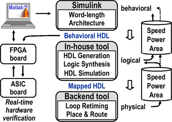
According to the introduction and analysis above, the technical utilization of the architecture relies heavily on computer-aided tools. Most existing aids convert hardware description languages such as Verilog and VHDL RTL code to gate-level code, such as ASIC CAD. While some theoretical work has been done in creating "reconfigurable" processing and advancing the use of discrete FPGA devices and enabling algorithm acceleration based on this, it is still early days for commercial tools and practical applications. But there are already companies promoting commercialization. FPGA vendors and EDA companies are teaming up to promote a standard set of megafunctions, or library of parameterized modules, or LPM, that can be directly recognized and translated by auxiliary tools [6]. If this goal can be achieved, then the code to design the FPGA prototype and the ASIC will be exactly the same. This means that the time required to convert between the two technologies will be 0, but the conversion between the two is still dependent on the architecture chosen by the designer.
The benefits of FPGA design at the architectural level are rapidly breaking the boundaries between programmable and fixed-function markets. There is a great deal of work and research surrounding the translation of abstract theory and laboratory findings into practical commercial use, such as design logic and C-like design languages [7][8][9]. There are also many architectural solutions similar to those described above [10][11]. In general, this attempt is still in the laboratory stage, and CAD does not have the matching function to perfect the idea.
3.2. Mapping transformation
|
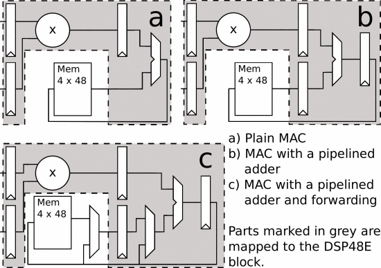
Figure 7. Hybrid ASIC/FPGA Flow. |
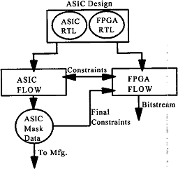
In recent years, there have been more and more schemes to use FPGA systems to make ASIC prototypes to complete ASIC verification. Due to the rapid growth of ASIC tape-out cost and design cost, the current typical 90nm SOC design tape-out cost is estimated to be about 1 M. This reflects the importance of using FPGA systems to avoid repeated iterations [12].
Mapping means converting ASIC primitives to FPGA logic cells during the design process in order to reverse the conversion, so the main means is the similar component interoperability transformation. The mapping process requires attention to the issues given below.
The utilization of each partition should be fully considered when designing a prototype with an FPGA system. Although there are many auxiliary tools that can automatically give the partition plan, the automatically given partition sometimes does not meet the specific needs of the prototype. Therefore, a graphical input tool should be used to manage architectural-level zoning planning. Take the FPGA as a module in the design process, and adjust the module according to the needs to meet the designers' requirements for verification and modification.
As mentioned above, the mapping process of the MAC module can be used as an example. A straightforward but inefficient mapping scheme is given in Figure 7a due to the inability to interact with the accumulation registers in the DSP48E. Another improved scheme is shown in 7b, where the adders of the pipelined MAC module have been well mapped into the DSP48E. But another problem arises that the same register cannot receive all the pipelines. Then Figure 7c gives the final solution and the way we would like to see the mapping. It avoids the functional problems caused by direct mapping while relatively improving the performance of the MAC and the DSP48E.
|
Figure 8. MAC units mapped to DSP48E blocks. |
Gated clocks should be avoided in the design of FPGA template systems. Clock gates are used in ASIC to power down the clock tree when needed to save power and extend the life of portable device power supplies. However, gated clocks can slow down operations in FPGA because most FPGA require higher-speed, low-skew clock inputs.
The time and economic costs are increasing, and the more efficient and effective conversion of FPGA systems into ASIC is recognized by more and more people. coding, SDC support, specific and identical function libraries, and other issues that need to be considered when designing. Using existing technology to apply a more convenient design method to ASIC is an economical way to expand and supplement. There have been many advances in software algorithms in recent years, but these hardware and software systems have no templates and are used ad hoc. Considering the dependencies, we still need to focus on developing a set of software aids that can automatically map transformations.
4. Conclusion
The cost of design tape-out is increasing as global supply chains are blocked. The addition of an FPGA system greatly simplifies the design process of an ASIC. Embedding FPGA units at the architectural level can improve design flexibility, allowing designers more freedom to modify and adjust the modules after simulation instead of restarting iterations. Meanwhile, the addition of small cells increases area utilization, providing improvements in economics. The embedded FPGA can also make up for the data gap and increase the channel to improve the operation speed. Thanks to the interoperable front-end platform and hardware description language, FPGA and ASIC can be converted into each other under a special design environment such as a special architecture. When two otherwise distinct technologies can be seamlessly translated into each other, it provides huge time advantages and cost savings.
Overall, we need an automated mapping system that goes beyond existing tools to revolutionize the industry. The new system requires strong interoperability and a library of functions that can describe both circuits at the same time.
References
[1]. Balboni, A., Valenti, L. (1996). ASIC design and FPGA design: A unified design methodology applied to different technologies. In: Hartenstein, R.W., Glesner, M. (eds) Field-Programmable Logic Smart Applications, New Paradigms and Compilers. FPL 1996. Lecture Notes in Computer Science, vol 1142. Springer, Berlin, Heidelberg. https://doi.org/10.1007/3-540-61730-2_38
[2]. R. Madurawe (2010), "3D FPGA & 3D ASIC worlds first unified 3D IC design platform," 2010 IEEE Hot Chips 22 Symposium (HCS), 2010, pp. 1-16, doi: 10.1109/HOTCHIPS.2010.7480079.
[3]. O. Melnikova, I. Hahanova and K. Mostovaya, "Using multi-FPGA systems for ASIC prototyping," 2009 10th International Conference - The Experience of Designing and Application of CAD Systems in Microelectronics, 2009, pp. 237-239.
[4]. T. Sato, S. Chivapreecha, P. Moungnoul and K. Higuchi (2016), "An FPGA Architecture for ASIC-FPGA Co-design to Streamline Processing of IDSs," 2016 International Conference on Collaboration Technologies and Systems (CTS), 2016, pp. 412-417, doi: 10.1109/CTS.2016.0079.
[5]. T. Sato, S. Chivapreecha, P. Moungnoul and K. Higuchi, "RCA on FPGAs Designed by the RTL Design Methodology and Wave-Pipelined Operation", Proc. of ECTI-CON 21016, pp. 1251.1-1251.6, 2016.
[6]. Buist, R. H. (1999). FPGA/ASIC design software. Ecn, 43(3), 115. Retrieved from https://www.proquest.com/trade-journals/fpga-asic-design-software/docview/222217476/se-2?accountid=153081
[7]. Ahi Alex Ye, Nagaraj Shenoy and Prithviraj Banerjee, "A C Compiler for a Processor with a Reconfigurable Functional Unit", Proceedings of the 37th ACM/IEEE conference on Design automation conference, 2000. Retrieved from https://doi.org/10.1145/329166.329187
[8]. Meenakshi Kaul, Ranga Vemuri, Sriram Govindarajan and Iyad Ouaiss, "An Automated Temporal Partitioning and Loop Fission approach for FPGA based reconfigurable synthesis of DSP applications", Proceedings of the 36th ACM/IEEE conference on Design automation conference, pp. 616-622, 1999. Retrieved from https://doi.org/10.1145/337292.337581
[9]. Brad L. Hutchings and Brent E. Nelson, "Using General-Purpose Programming Languages for FPGA Design", Proceedings of the 37th ACM/IEEE conference on Design automation conference, pp. 561-566, 2000. Retrieved from https://doi.org/10.1145/309847.310010
[10]. Masakazu Yarnashina and Masato Motomura, "Reeonfigurable Computing: Its Concept and a Practical Embodiment using Newly Developed Dynamically Reconfigurable Logic (DRL) LSI", Proceedings on the 2000 conference on Asia and South Pacific design automation, pp. 329-332, 2000. Retrieved from https://doi.org/10.1145/368434.368659
[11]. Norben Imlig, Ryusuke Konishi, Tsunemichi Shiozawa, Kiyoshi Oguri, Kouichi Nagami, Hideyuki Ito, et al., "Communicating Logic: An Alternative Embedded Stream Processing Paradig", Proceedings of the ASP-DAC 2000, pp. 317-322, 2000. Retrieved from https://doi.org/10.1145/368434.368666
[12]. M. Santarini, "ASIC prototyping: make versus buy", EDN, Dec. 2005. Retrieved from https://www.researchgate.net/publication/292859931_ASIC_prototyping_Make_versus_buy
Cite this article
Lei,X. (2023). Review on the FPGA design optimization for ASIC. Applied and Computational Engineering,4,524-531.
Data availability
The datasets used and/or analyzed during the current study will be available from the authors upon reasonable request.
Disclaimer/Publisher's Note
The statements, opinions and data contained in all publications are solely those of the individual author(s) and contributor(s) and not of EWA Publishing and/or the editor(s). EWA Publishing and/or the editor(s) disclaim responsibility for any injury to people or property resulting from any ideas, methods, instructions or products referred to in the content.
About volume
Volume title: Proceedings of the 3rd International Conference on Signal Processing and Machine Learning
© 2024 by the author(s). Licensee EWA Publishing, Oxford, UK. This article is an open access article distributed under the terms and
conditions of the Creative Commons Attribution (CC BY) license. Authors who
publish this series agree to the following terms:
1. Authors retain copyright and grant the series right of first publication with the work simultaneously licensed under a Creative Commons
Attribution License that allows others to share the work with an acknowledgment of the work's authorship and initial publication in this
series.
2. Authors are able to enter into separate, additional contractual arrangements for the non-exclusive distribution of the series's published
version of the work (e.g., post it to an institutional repository or publish it in a book), with an acknowledgment of its initial
publication in this series.
3. Authors are permitted and encouraged to post their work online (e.g., in institutional repositories or on their website) prior to and
during the submission process, as it can lead to productive exchanges, as well as earlier and greater citation of published work (See
Open access policy for details).
References
[1]. Balboni, A., Valenti, L. (1996). ASIC design and FPGA design: A unified design methodology applied to different technologies. In: Hartenstein, R.W., Glesner, M. (eds) Field-Programmable Logic Smart Applications, New Paradigms and Compilers. FPL 1996. Lecture Notes in Computer Science, vol 1142. Springer, Berlin, Heidelberg. https://doi.org/10.1007/3-540-61730-2_38
[2]. R. Madurawe (2010), "3D FPGA & 3D ASIC worlds first unified 3D IC design platform," 2010 IEEE Hot Chips 22 Symposium (HCS), 2010, pp. 1-16, doi: 10.1109/HOTCHIPS.2010.7480079.
[3]. O. Melnikova, I. Hahanova and K. Mostovaya, "Using multi-FPGA systems for ASIC prototyping," 2009 10th International Conference - The Experience of Designing and Application of CAD Systems in Microelectronics, 2009, pp. 237-239.
[4]. T. Sato, S. Chivapreecha, P. Moungnoul and K. Higuchi (2016), "An FPGA Architecture for ASIC-FPGA Co-design to Streamline Processing of IDSs," 2016 International Conference on Collaboration Technologies and Systems (CTS), 2016, pp. 412-417, doi: 10.1109/CTS.2016.0079.
[5]. T. Sato, S. Chivapreecha, P. Moungnoul and K. Higuchi, "RCA on FPGAs Designed by the RTL Design Methodology and Wave-Pipelined Operation", Proc. of ECTI-CON 21016, pp. 1251.1-1251.6, 2016.
[6]. Buist, R. H. (1999). FPGA/ASIC design software. Ecn, 43(3), 115. Retrieved from https://www.proquest.com/trade-journals/fpga-asic-design-software/docview/222217476/se-2?accountid=153081
[7]. Ahi Alex Ye, Nagaraj Shenoy and Prithviraj Banerjee, "A C Compiler for a Processor with a Reconfigurable Functional Unit", Proceedings of the 37th ACM/IEEE conference on Design automation conference, 2000. Retrieved from https://doi.org/10.1145/329166.329187
[8]. Meenakshi Kaul, Ranga Vemuri, Sriram Govindarajan and Iyad Ouaiss, "An Automated Temporal Partitioning and Loop Fission approach for FPGA based reconfigurable synthesis of DSP applications", Proceedings of the 36th ACM/IEEE conference on Design automation conference, pp. 616-622, 1999. Retrieved from https://doi.org/10.1145/337292.337581
[9]. Brad L. Hutchings and Brent E. Nelson, "Using General-Purpose Programming Languages for FPGA Design", Proceedings of the 37th ACM/IEEE conference on Design automation conference, pp. 561-566, 2000. Retrieved from https://doi.org/10.1145/309847.310010
[10]. Masakazu Yarnashina and Masato Motomura, "Reeonfigurable Computing: Its Concept and a Practical Embodiment using Newly Developed Dynamically Reconfigurable Logic (DRL) LSI", Proceedings on the 2000 conference on Asia and South Pacific design automation, pp. 329-332, 2000. Retrieved from https://doi.org/10.1145/368434.368659
[11]. Norben Imlig, Ryusuke Konishi, Tsunemichi Shiozawa, Kiyoshi Oguri, Kouichi Nagami, Hideyuki Ito, et al., "Communicating Logic: An Alternative Embedded Stream Processing Paradig", Proceedings of the ASP-DAC 2000, pp. 317-322, 2000. Retrieved from https://doi.org/10.1145/368434.368666
[12]. M. Santarini, "ASIC prototyping: make versus buy", EDN, Dec. 2005. Retrieved from https://www.researchgate.net/publication/292859931_ASIC_prototyping_Make_versus_buy