


1. Introduction
With the rapid advancement of technology in the electronics industry, there is an increasing demand for lightweight, cost-effective, highly flexible optoelectronic devices that are compatible with large surface areas. These next-generation devices can be affixed to soft surfaces, including human skin, thereby enabling a wide range of wearable and portable functionalities. Perovskite materials have emerged as promising candidates for next-generation optoelectronic applications due to their exceptional photoelectric properties. These include long carrier diffusion lengths, low Urbach energies, high absorption coefficients, tunable band gaps, and small exciton binding energies. Photodetectors play a crucial role in numerous applications; perovskite materials-characterized by their high optical absorption coefficients and excellent carrier mobilities—facilitate the efficient conversion of optical signals into electrical signals. In comparison to traditional silicon (Si) materials, perovskites exhibit superior light absorption characteristics. Furthermore, by modifying their composition (such as varying cations or halogens), it is possible to adjust the band gap of perovskite materials. This tunability allows optimization across different spectral bands to meet diverse light detection requirements encompassing ultraviolet light, visible light, and near-infrared radiation.
At present, the development trend of photodetectors is oriented towards higher frequency response and flexible applications. On one hand, perovskite photodetectors are well-suited to meet these response requirements due to their high photoelectric conversion efficiency, low manufacturing costs, and adjustable band gap. Additionally, the tunability of their crystal structure (such as the ABX3 configuration) enables optimization of the spectral response range, resulting in rapid response speeds that make them widely applicable in optical communications, sensors, and imaging technologies. On the other hand, while perovskite materials exhibit good flexibility and plasticity when fabricated on a flexible substrate, issues related to reliability and fatigue continue to hinder the widespread adoption of this technology for flexible applications due to inherent brittleness. Therefore, there is an urgent need for further research and exploration aimed at addressing the challenges faced by flexible devices.
In recent years, high-performance photodetectors have attracted much attention due to their important applications in imaging, spectroscopy, fiber optic communications, remote control, and chemical/biological sensing. Nano-structured perovskite is an ideal material for detection because of its long carrier lifetime, high carrier mobility, easy synthesis and miniaturization. These devices exhibit high optical responsiveness, large external quantum efficiency (EQE), significant gain, high detectability, and fast response times. For example, Song et al. first reported the preparation of atomically thin two-dimensional CsPbBr3 nanosheets and demonstrated their superior performance when used in flexible photodetectors after solution treatment. Ultraviolet-visible absorption spectra of CsPbBr3 nanosheets show good absorption capacity with a direct band gap of about 2.32 electron volts. The flexible photodetector has a high switching ratio (>103), indicating that it has excellent optical switching characteristics, while exhibiting high responsiveness (0.25A W-1) and a peak EQE value of 53%, indicating that CsPbBr3 nanosheets have great potential in high-sensitivity detectors. However, due to the poor charge transport performance of perovskite materials themselves, resulting in insufficient responsiveness, it is necessary to combine perovskite with high mobility materials to improve their responsiveness. In the field of nano-perovskite photodetectors, researchers are ushering in revolutionary application development prospects that enable them to significantly regulate the size, shape and composition of perovskite nanomaterials to achieve unprecedented performance improvements. These improvements not only provide better stability, but also enhanced optical response, sensitivity, and spectral tunability. However, a number of key challenges, including environmental stability, manufacturing scalability, and toxicity issues, still need to be addressed before widespread commercial use.
This paper aims to comprehensively analyze the properties and applications of nanoscale perovskites, which is a key challenge in developing this promising new functional material. In this paper, various synthesis methods of nano-scale perovskites are first examined, ranging from traditional methods such as hydrothermal methods to more advanced techniques such as vapor deposition. These methods will be described in detail and the properties of nano-scale perovskites synthesized in this way will be demonstrated. Therefore, this paper will conduct comparative evaluation and analysis of these nano-scale perovskites to highlight their advantages and limitations, and finally make a complete summary of the advantages and disadvantages of various nano-scale perovskites.
2. Design & fabrication
Nanostructures represent a significant structural form in materials science, characterized by their unique advantages and potential applications across various fields. First and foremost, one of the primary benefits of nanostructures lies in their distinctive physical and chemical properties. Due to the size-dependent effects inherent in nanomaterials, such as quantum size effects, surface effects, and local phenomena-nanostructured materials often display markedly different characteristics compared with their macroscopic counterparts. Furthermore, these nanomaterials exhibit exceptional magnetic, optical, and electrical properties, which contribute to their promising application prospects in optoelectronic devices, sensors, and catalysts. Secondly, nanostructures are also recognized for their outstanding mechanical properties. At the nanoscale level, the mechanical behavior of materials is intricately linked to their crystal structure and grain boundary dynamics. Thanks to attributes such as high surface area and improved lattice structures, nanomaterials frequently demonstrate superior mechanical performance—including high strength, elevated hardness, and remarkable toughness. In this paper, an analysis of various types of nanostructures including perovskite quantum dots, nanorods, nanoribbons, and nanosheets.
Quantum dots (QDs) are composed of a finite number of atoms, all three dimensions on the order of nanometers. Quantum dots are generally spherical or quasi-spherical and are nanoparticles with a stable diameter of 2 ~ 20 nil2 made of semiconductor materials (usually composed of elements IIB ~ VI B or IIIB ~ VB). Quantum dots are collections of atoms and molecules on the nanoscale, which can be composed of either one semiconductor material, such as group II.VI elements (such as CdS, CdSe, CdTe, ZnSe, etc.) or Group III.V elements (such as InP, InAs, etc.), or two or more semiconductor materials.
Nanorods are one-dimensional nanomaterials, but compared with nanoribbons and nanowire, nanorods are shorter in the length direction, generally up to several hundred nanometers, the ratio of length to diameter is about 3-5, and the cross-section shape is circular or polygonal.
The nanoribbons have a rectangular interface, the thickness is in the order of nanometers, the width can reach hundreds of nanometers, the width is relatively large, and it is a very thin elongated structure.
Nanosheet refers to the sheet structure with nanometer thickness, usually refers to the thickness of the nanometer scale and the length and width of the sheet structure is much larger than the thickness; Compared with the flat ribbon structure of the nanoribbons, there is a larger thickness.
3. Analysis & challenge
3.1. Quantum dots
In general, there are two well-established methods for the preparation of perovskite quantum dots: thermal injection and ligand-assisted reprecipitation. The thermal injection process is conducted at elevated reaction temperatures within an inert atmosphere. Typically, perovskite quantum dots are synthesized by rapidly injecting cesium oleate into a solution containing lead halide (PbX2), oleic acid (OA), and oleamine (OAm) at high temperatures [1, 2]. In this process, OA chelates with lead atoms on the surface, while OAm interacts with halide atoms present on the surface. A recent study by Zou et al. successfully prepared CsPbI3 quantum dots using thermal injection. The morphological characteristics revealed through scanning electron microscopy (SEM), atomic force microscopy (AFM), and transmission electron microscopy (TEM) indicate that CsPbI3 produced via this method exhibits a film with virtually no pinholes and a remarkably smooth surface [3]. This quality can be attributed to the uniform size and orderly arrangement of the quantum dots as illustrated in Figure 1a-c. Ligand-assisted reprecipitation (LARP), also referred to as suprasaturated recrystallization (SR), is performed at room temperature (RT) under atmospheric pressure [4]. With this method, quantum dots can be synthesized within minutes and scaled up to gram-scale production. Typically, inorganic salts, organic acids, and amines are dissolved in a highly polar solvent such as DMF (dimethylformamide), after which a precise volume of this precursor solution is introduced into a non-polar solvent like toluene. The significant solubility difference of inorganic salts between DMF and toluene facilitates rapid recrystallization (Figure 1d). Furthermore, LARP (Liquid-Assisted Reprecipitation) technology can be optimized for the preparation of colloidal quantum dots. Dai et al. explored the influence of various ligands on colloidal quantum dot formation [5]. They substituted oleic acid (OA) with 3-phenyl-2-propenylamine (PPA) and discovered that MAPbBr3 quantum dots with the desired crystal structure could be controllably formed using conjugated PPA ligands. As illustrated in Figures 1e and f, quantum dot films incorporating conjugated polyacrylic acid (PAA) ligands demonstrate enhanced electrical conductivity due to the dispersion of molecular orbitals. This research offers an effective strategy for enhancing both the conductivity and colloidal stability of quantum dots, which are crucial for diverse optoelectronic applications.
Perovskite quantum dots (QDs) are of significant interest due to their unique properties and potential applications. These microscopic crystals are synthesized through intricate processes that regulate their formation and growth rates, resulting in uniform quantum dots with sizes ranging from 3 to over 13 nanometers. Their absorption spectra can reveal up to four exciton levels, the characteristics of size and shape determine their overall properties[6]. These quantum dots exhibit variable electrical and optical properties, making them suitable for a wide array of applications including solar cells, light-emitting diodes (LEDs), catalysis, sensing, imaging, and lasers [7]. Furthermore, their synthesis occurs at room temperature, allowing for precise control over the size and composition of the spherical quantum dots produced. The emission colors of these quantum dots vary depending on their size, facilitating efficient light emission. Additionally, by adjusting the halide ratio and doping at the B position within the structure, it is possible to finely tune the emission wavelength [7,8].
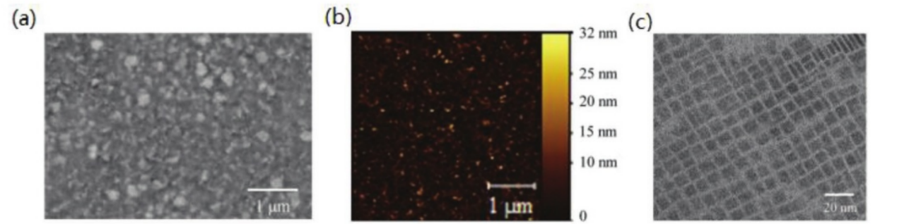
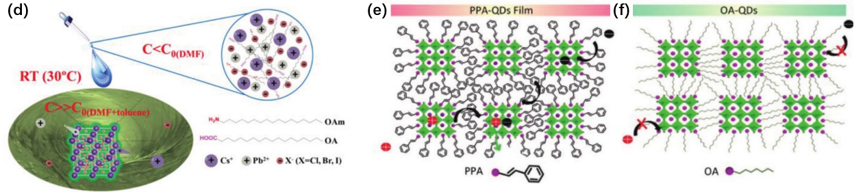
Figure 1: a) Top view SEM image of the CsPbI3 QD thin fflm coated on the DPP-DTT layer. There is no obvious pinhole in the perovskite QD fflm. b) AFM surface roughness image of the CsPbI3 QD fflm in a 4 × 4 µm2 region, the root-mean-square roughness is extracted to be 3.6 nm. c) TEM image of the synthesized CsPbI3 QDs. Reproduced with permission. d) The SR can be finished within 10 s through transferring the Cs+, Pb2+, and X- ions from the soluble to insoluble solvents at RT without any protecting atmosphere and heating. C: ion concentration in different solvents. C0: saturated solubilities in DMF, toluene, or mixed solvents (DMF+ toluene). e,f) Illustration of carrier transport in different QDs films (PPA-QDs and OA-QDs).[2].
However, quantum dots also have their disadvantages: First, their synthesis conditions are very demanding, requiring nucleation under high temperature, no oxygen, no water conditions. Although it is already possible to synthesize quantum dots at room temperature or in water, it still requires an oxygen-free environment. In addition, quantum dots are not water-soluble, tend to aggregate and have toxic side effects on organisms, and are not easy to surface modification.
3.2. Nanorod
In general, the preparation method for nanorods primarily involves hydrothermal technique. For instance, a typical synthesis method for CsPbBr3 perovskite nanorods is illustrated in Figure 2(a) [9]. In this procedure, 10 mL of In (OAm)3 solution and 6 mL of CsPbBr3 stock solution are combined in a 50 mL three-neck flask and mixed under a nitrogen atmosphere for 10 minutes. Subsequently, 0.14 mL of TDP ligand is injected into the mixture, which is then heated to 50 °C at a rate of 10 °C/min. Once the solution becomes colorless, the temperature is further increased to 100 °C. The resulting mixture is then cooled using an ice water bath to yield a crude solution of CsPbBr3 nanorods. The crude solution containing CsPbBr3 nanorods is subsequently added to triply distilled ethyl acetate and centrifuged at a speed of 7000 r/min for 3 minutes. After discarding the supernatant, the precipitate is dissolved in ethane. This process is repeated several times; ultimately, purified droplets from this solution are deposited onto silicon wafers to create test samples.
The CsPbBr3 perovskite nanorods exhibit not only remarkable optical properties but also high stability in amplified spontaneous emission (ASE). The UV-VIS absorption spectra and photoluminescence (PL) spectra of the CsPbBr3 perovskite nanorod sample at room temperature are presented in Figure 2(b). The exciton absorption peak is observed at 504 nm, while the PL peak occurs at 518 nm. Notably, the PL peak experiences a redshift of 14 nm compared to the exciton absorption peak. This small Stokes shift can be attributed to minimal energy loss resulting from non-radiative recombination.
As illustrated in Figure 2(c), a laser with a wavelength of 355 nm and a pulse width of 1 ns was employed to continuously excite the sample under ambient temperature and humidity conditions (T = 23 °C, RH = 40%). The ASE intensity exhibited minimal variation over a period of 300 minutes, demonstrating remarkable stability. To evaluate the stability of the sample under extreme aging conditions, we assessed the luminescence stability of CsPbBr3 perovskite nanorods at elevated temperature and high humidity (relative humidity = 85%, temperature = 85 °C). The results are presented in Figure 2(d). The sample was placed in an aging chamber where both temperature and humidity were maintained constantly. Photoluminescence (PL) strength was measured every hour, with results compared to those obtained from CsPbBr3 nanocrystal samples synthesized using OA and OAm ligands. After continuous aging for 180 minutes, the PL strength of CsPbBr3 nanocrystalline samples had nearly diminished completely; conversely, CsPbBr3 perovskite nanorods retained approximately 60% of their initial strength even after enduring for up to 300 minutes. This finding indicates that CsPbBr3 perovskite nanorods not only exhibit superior ASE stability but also demonstrate enhanced resilience compared to CsPbBr3 perovskite nanocrystalline samples when subjected to high humidity and elevated temperatures.
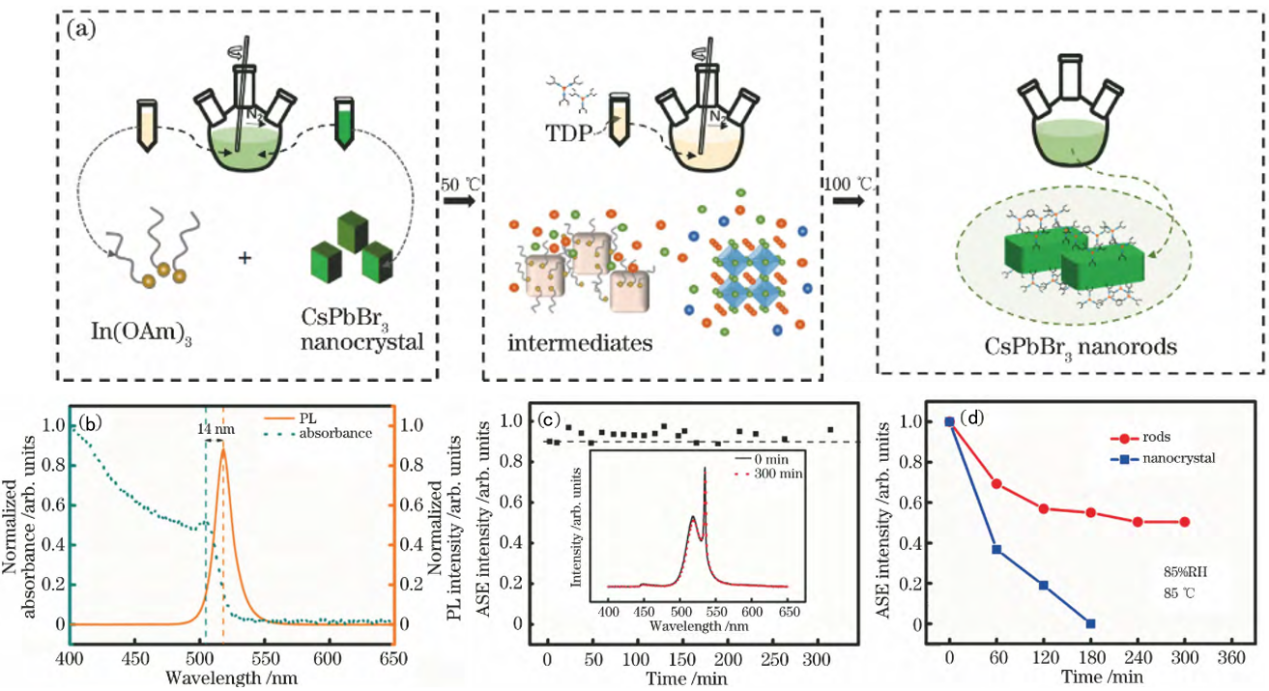
Figure 2: (a)Sample preparation flowchart of CsPbBr3 perovskite nanorods. (b)Absorption spectra and PL spectra of CsPbBr3 nanorods. (c) ASE stability of the nanorods material; (d) comparison between PL intensity stability of the CsPbBr3 perovskite nanorods and nanocrystal after aging experiment (under 85% RH at 85 °C )[10].
Perovskite nanorods have higher crystal quality and better luminescence characteristics, which reduce the atomic suspended surface bonds and surface defects on the crystal surface, but their production process is complicated and slow, and there is a high demand for materials.
3.3. Nanoribbon
The synthesis of two-dimensional CsPbBr3 perovskites was conducted as detailed in the experimental section (Figure 3(a)). In contrast to the commonly employed supersaturated recrystallization method, this experiment utilizes octane as the antisolvent instead of toluene [11]. In this approach, cesium and lead precursors are dispersed in octane and N,n-dimethylformamide (DMF), respectively. Unlike toluene, octane is immiscible with DMF, allowing for the separation of cesium and leading precursors into distinct phases. The addition of oleic acid (OA) as a surfactant facilitates the formation of a microemulsion within the reaction system [12]. This design significantly diminishes the likelihood of contact between cesium and lead precursors, thereby reducing the supersaturation level within the reaction environment. Consequently, during the initial phase of the reaction, only a limited number of nuclei are generated while most reactants are consumed during growth, resulting in products with larger dimensions. The morphology of these products was characterized by using transmission electron microscopy (TEM). As illustrated in Figures 3b-e at various magnifications, TEM images reveal that the product exhibits a zonal shape with transverse sizes reaching micron levels. Extending the reaction time further increases these transverse dimensions. When toluene is substituted for octane while maintaining other experimental parameters constant, there is a notable reduction in product size (Fig. 3f). This phenomenon occurs because when miscible toluene is combined with DMF, there is an abrupt increase in system supersaturation leading to an abundance of nuclei formation. With a fixed total amount of reactants but an increased number of nuclei present, average growth per nucleus decreases substantially. As a result, reactants become depleted more rapidly and yield predominantly smaller-sized products.
The scanning electron microscopy (SEM) analysis of the sample provided a comprehensive overview of its morphology, highlighting the ultra-thin thickness and flexibility of the two-dimensional CsPbBr3 nanoribbons (Fig. 3g, h). In nanostructures synthesized via colloidal methods, the organic ligands present on their surfaces play a pivotal role in ensuring stability and facilitating functionalization. Fourier transform infrared spectroscopy (FTIR) was employed to ascertain the surface chemical composition of the two-dimensional CsPbBr3 nanoribbons. As illustrated in Figure 3i, prominent peaks at 1570 cm⁻¹ are attributed to N−H shear vibrations, while peaks at 810 cm⁻¹ and 1010 cm⁻¹ correspond to swaying and stretching vibrations of the amino group, respectively, indicating the presence of oleylamine (Ola). A characteristic strong and broad peak around 3100 cm⁻¹ is associated with tensile vibrations of protonated amino groups, suggesting that Ola exists in its protonated form. This observation aligns with previous reports regarding surface ligands on CsPbBr3 nanocrystals; where protonated Ola not only serves as a capping ligand but also functions as a univalent ion embedded within the outer lattice, effectively substituting for cesium ions. It is noteworthy that although oleic acid (OA) was utilized during the initial stages of synthesis, no distinctive vibrational peak indicative of carboxylic acid was detected. This finding implies that following protonation, Ola transforms into a strongly binding ligand which significantly inhibits OA coordination with the nanoribbons—thereby establishing itself as the predominant ligand on their surface.
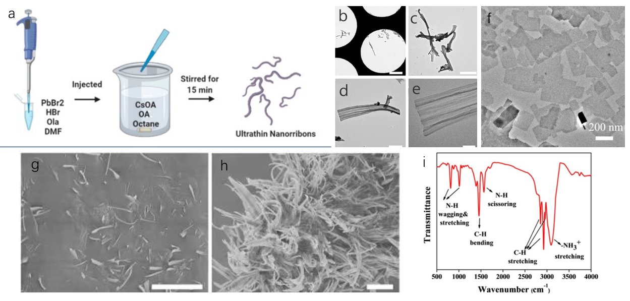
Figure 3: (a) Schematic Illustration of the Synthesis of Ultrathin CsPbBr3 Nanoribbons.(b-e)TEM images of CsPbBr3 nanoribbons at different magnifications. The scale bars are 20 μm (panel b), 5 μm (panel c), 2 μm (panel d), and 500 nm (panel e).(f) TEM image of the product using toluene as the anti-solvent.(g-h) SEM images at different magnification of CsPbBr3 nanoribbons obtained after 15 min reaction.(i) Fourier transform infrared spectrum of two-dimensional CsPbBr3 [11].
There are two disadvantages of two-dimensional CsPbBr3 perovskite nanoribbons[11]. One is that the thickness is thinner in the direction parallel to the electron beam, and the diffraction signal is relatively weak. In addition, the expansion of the perovskite lattice due to the two-dimensional structure causes the X-ray diffraction (XRD) peak to shift slightly to the lower Angle compared to the standard PDF (54-0752).
3.4. Nanosheet
Wang et al. reported the colloidal synthesis of CsPb2Br5 nanosheets (NSs) utilizing a straightforward precipitation method, wherein inorganic cations Cs+ were employed to replace the organic methylammonium (MA) [13]. They discovered that a relatively small quantity of the surfactant cetylammonium bromide (HA), characterized by its short carbon chain, can effectively initiate the formation of CsPb2Br5 NSs. During the synthesis process, a DMF solution containing PbBr2 and cetylammonium bromide is introduced into toluene to create a mixture; subsequently, a suspension of CsBr in DMF is added to this pre-prepared toluene mixture under vigorous agitation. The authors investigated various reaction precursors to elucidate how ions influence the precipitation of CsPb2Br5 (where X = Cl-, Br-, or I-) nanosheets. Figure 4 illustrates the morphology of perovskite nanosheets with differing compositions. Figures 4(a) and (b) depict a typical two-dimensional NS structure, while Figures 4c and d reveal an irregular arrangement of particles or plates, indicating that both CsPb2Br5-x Clx and CsPb2Br5-xIx NSs were successfully synthesized using this approach.
The advantages of nanoribbons include simple and scalable processes suitable for general-purpose applications with customizable properties [14], as well as high sensitivity, enhanced responsiveness, and thin uniform sheets adaptable to various perovskite compositions [15].
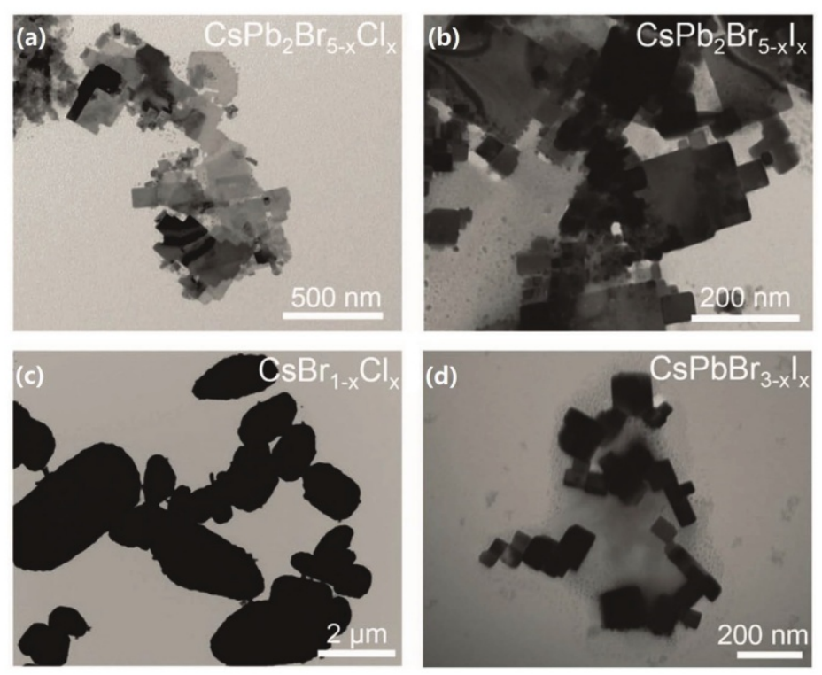
Figure 4: a–d) TEM images showing the representative nanostructures of CsPb2Br5-xClx, CsPb2Br5-xIx, CsBr1-xClx, and CsPbBr3-xIx, respectively. Reproduced with permission.
Nanosheets are susceptible to contamination, face high manufacturing costs, exhibit low yields, and pose safety concerns. Challenges remain in the preparation technology; physical methods of preparation necessitate the use of expensive equipment and gases, leading to significant energy consumption and consequently elevated production costs. The chemical preparation method involves a variety of chemicals that impose stringent safety requirements on laboratory environments, thereby increasing operational complexity and risk. Given that the preparation process is typically intricate and entails numerous precise experimental operations and control techniques, the size, shape, and distribution of nanoparticles significantly influence their properties. Therefore, it is essential to maintain meticulous control over the preparation conditions.
4. Summary & Suggestion
Table 1: Comparison of different nanostructure of perovskite photodetectors.
Type | Advantages | Disadvantages |
Quantum dot | High luminosity, size and shape control, good crystal quality, high sensitivity and responsiveness stability and reproducibility, high quantum yield narrow size distribution | Complex equipment setup, mass production variability, shape and size inconsistencies, solvent residues |
Nanorod | Higher crystal quality and better luminous characteristics, extremely high gain coefficient and low ASE threshold, better luminous stability | The production process is complex and slow, and the requirements for materials are high |
Nanosheet | High crystallinity, uniform thickness, customized performance, simple and low-cost atmospheric environment manufacturing process, enhanced light detection stability and durability | Vulnerable to contamination, high manufacturing costs, low yield and safety issues |
Nanoribbon | The material has stable properties, large surface area, small number of crystal nuclei, promoting the consumption of reactants for growth, and good fluorescence properties | The service life is short, the adhesion is weakened after long-term use, and needs to be replaced |
The Summary of the 4 types of perovskites nano-materials were compared in Table 1.
The perovskite quantum dots synthesized through hot injection technology exhibit several advantages, including high luminosity and excellent crystal quality that can be controlled by size and shape. The resulting devices demonstrate high sensitivity, responsiveness, stability, and reproducibility, along with distinctive features such as a high quantum yield and narrow size distribution. However, this method also presents challenges related to complexity in equipment setup and variability in mass production. In contrast, the synthesis of perovskite quantum dots via ligand-assisted precipitation offers benefits such as simplicity and scalability. This approach utilizes universal solvents and enables the fabrication of devices with a broad spectral response while being cost-effective. Additionally, it allows for flexible combinations in production at low costs. Nevertheless, challenges remain concerning inconsistencies in shape and size as well as potential solvent residues.
Through the characterization of material morphology and optical properties, it has been determined that perovskite nanorods exhibit superior crystal quality and enhanced luminescence characteristics. The gain coefficient of CsPbBr3 nanorods was measured using the variable fringe length (VSL) method. Amplified spontaneous emission (ASE) phenomena were observed at room temperature. The results indicated that samples of CsPbBr3 nanorods possess a remarkably high gain coefficient and a low ASE threshold, demonstrating their significant potential as laser gain materials. The TDP branching ligands provide effective surface passivation, which reduces suspended atomic bonds and surface defects on the crystal surface. Additionally, their substantial steric hindrance contributes to preventing the degradation of perovskite materials in high humidity environments. In comparison to CsPbBr3 perovskite nanocrystalline samples, perovskite nanorods exhibit greater stability under conditions of elevated humidity and temperature. This enhanced stability can be attributed to two primary factors: 1) The slow growth rate of the nanorods allows sufficient time for atomic rearrangement, thereby reducing the density of defect states within the nanorods. This reduction minimizes non-radiative recombination caused by defects while also decreasing electron capture and scattering centers; 2) The presence of TDP ligands on the surfaces of the nanorods imparts a branched-chain structure with stronger steric hindrance compared to traditional ligands such as oleic acid (OA) and octylamine (OAm). Consequently, this structural advantage enables CsPbBr3 nanorods to maintain higher stability in environments characterized by elevated temperatures and humidity. Given these numerous advantages, it is evident that the synthesis process for perovskite nanorods is highly refined; however, this complexity results in a production process that is both intricate and time-consuming while imposing stringent requirements on raw materials.
In experiments, high-resolution scanning was performed on the edges of the substrate covered with nanoribbons. The scanning results showed that the edge was indeed laid flat on the substrate and was 3.5 nm thick in the vertical direction, inferring that the actual thickness of the nanoribbon was 3.5 nm. After 30 hours under environmental conditions (25°C and about 30% relative humidity), the PL peak of the nanoribbons remained unchanged, and the maximum of the original PL strength was halved, indicating that their chemical stability was better than that of small-sized nanoplates of the same thickness. Under the action of strong ultraviolet light, their fluorescence emission peak is redshifted due to photoaggregation and growth, which is comparable to other nanostructures with similar thickness. Compared to the standard PDF (54-0752), the X-ray diffraction (XRD) peaks are slightly shifted towards the lower Angle, which is attributed to the expansion of the perovskite lattice due to the two-dimensional structure.
The nanosheets produced through solution tank stripping exhibit high sensitivity and enhanced responsiveness. Their unique characteristics, including thinness and uniformity, allow them to adapt effectively to various perovskite compositions. Perovskite nanosheets possess excellent optical quality, with a small lateral size ranging from 5 to 10 µm and a thickness of less than 80 nm. This significantly reduces the diffusion distance of ions within the material, thereby improving the magnification performance of electrodes and facilitating rapid charge and discharge processes. Due to their extremely thin structure, these nanosheets offer a much larger surface area compared to conventional materials, making them highly effective in applications such as molecular release, adsorption, catalysis, among others. However, solvothermal nanosheets face challenges related to unstable solvent residues. Additionally, they are prone to contamination issues along with high manufacturing costs and low yields that raise safety concerns. There remain significant challenges in preparation technology; physical methods often necessitate expensive equipment and gases while consuming substantial energy resources—resulting in elevated production costs. Conversely, chemical preparation methods involve numerous chemicals that impose stringent laboratory safety requirements which further complicate operations and increase associated risks.
5. Conclusion
This paper investigates the properties, advantages, and disadvantages of perovskite under various nanostructures. It concludes that the synthesis difficulty ranks from most challenging to least challenging as follows: nanorods, nanofilms, nanoribbons, and quantum dots. In terms of flexibility, the order from highest to lowest is as follows: nanosheets, nanoribbons, quantum dots, and nanorods. Due to their two-dimensional structure, nanosheets exhibit excellent ductility and bending capabilities. Nanoribbons typically possess a narrow width coupled with a high aspect ratio, enabling them to endure bending and deformation to some extent. Conversely, quantum dots have a zero-dimensional structure (i.e., point-like), which may render them relatively less flexible compared to nanosheets or nanoribbons; thus they are more difficult to bend or stretch. Nanorods generally feature a one-dimensional structure (i.e., rod-like) and can withstand some degree of stretching or compression along their length; however, they are comparatively weaker in terms of bending or torsion. Regarding optical properties, different nanostructures present unique advantages: both quantum dots and nanoribbons demonstrate superior fluorescence characteristics alongside high fluorescence quantum yields. The nanorods exhibit superior luminescence stability and are less influenced by the longitudinal optical phonon-electron interaction, leading to a reduced unnecessary broadening of the photoluminescence (PL) beam width. The nanoribbons demonstrate enhanced water stability, maintaining their original monoclinic phase structure even after immersion in water. Furthermore, nanorods possess a higher gain coefficient and lower amplified spontaneous emission (ASE) threshold, which expands their range of potential applications. By employing immiscible octane as an antisolvent during supersaturation recrystallization, perovskite nanoribbons can significantly decrease the number of crystal nuclei. This process facilitates the consumption of reactants for growth and encourages the formation of larger-sized products. Partial curling and folding observed in these structures indicate the ultra-thin thickness of CsPbBr3 perovskite nanoribbons, resulting in blurred lattice edges in high-resolution transmission electron microscopy (HRTEM) images. Due to their two-dimensional nature, CsPbBr3 perovskite is thin along the direction parallel to the electron beam; consequently, its diffraction signal is relatively weak. In comparison with nanosheets, these materials offer improved thermal and chemical stability that allows them to maintain structural integrity and properties under extreme environmental conditions.
References
[1]. Li, C., Li, J., Li, Z., Zhang, H., Dang, Y., Kong & F. (2021). High-Performance Photodetectors Based on Nanostructured Perovskites. Nanomaterials. Nanomaterials 2021, 11(4), 1038; DOI:10.3390/nano11041038
[2]. Gu, H., Chen, S., & Zheng, Q. (2020). Emerging Perovskite Materials with Different Nanostructures for Photodetectors. Advanced Optical Materials. Advanced Optical Materials 2020, 9(5), 2001637; DOI:10.1002/adm.202001
[3]. Zou, C., Xi, Y., Huang, C., Keeler, E. G., Feng, T., Zhu, S., Pozzo, L. D., Lin, L. Y., A Highly Sensitive UV–vis–NIR All-Inorganic Perovskite Quantum Dot Phototransistor Based on a Layered Heterojunction. Advanced Optical Materials, 6(14),1800324.h DOI:10.1002/adom.201800324
[4]. Li, X., Wu, Y., Zhang, S., Cai, B., Gu, Y., Song, J., Zeng, H., CsPbX3 Quantum Dots for Lighting and Displays: Room-Temperature Synthesis, Photoluminescence Superiorities, Underlying Origins and White Light-Emitting Diodes. Advanced Functional Materials,26(15), 24352445. DOI:10.1002/adfm.201600109
[5]. Dai, J., Xi, J., Li, L., Zhao, J., Shi, Y., Zhang, W., Ran, C., Jiao, B., Hou, X., Duan, X., Wu, Z., Angew. Chemical., Charge Transport between Coupling Colloidal Perovskite Quantum Dots Assisted by Functional Conjugated Ligands. Angewandte Chemie International Edition,57(20),57545758; DOI:10.1002/anie.201801780
[6]. Akkerman, Q.A., Nguyen, T.P., Boehme, S.C., Montanarella, F., Dirin, D.N., Wechsler, P., Beiglbock, F., Raino, G., Erni, R., Katan, C., Even, J.,& Kovalenko, M.V., Controlling the nucleation and growth kinetics of lead halide perovskite quantum dots. Science 377, 1406–1412 (2022). DOI:10. 1126/ science. abq36 16
[7]. Zou, J., Li, M., Zhang, X., Zheng, W., Perovskite quantum dots: synthesis, applications, prospects, and challenges. Journal of Apply Physic (2022). DOI:10. 1063/5. 01264 96
[8]. Akman, E., Ozturk, T., Xiang, W., Sadegh, F., Prochowicz, D., Tavakoli, M.M., Yadav, P., Yilmaz, M., & Akin, S., The efect of B-site doping in all-inorganic C sPbIxBr3–x absorbers on the performance and stability of perovskite photovoltaics. Energy Environment Science 16, 372–403 (2023). DOI:10.1039/ d2ee01070d
[9]. Das, A., Dutta, S., Dutta, A., Guria, A., & Narayan, P. Chemically Tailoring the Dopant Emission inManganese-Doped CsPbCl3 Perovskite Nanocrystals[J]. Angewandte Chemie International Edition, 2017, 56(30): 8746-8750.
[10]. Shi, Y., Li, R., Yu, J., Wang, S., Yang, X., & Chen, R. Synthesis and Stability of CsPbBr3 Perovskite Nanorods with High Optical Gain[J]. Chinese Journal of Lasers, 2020, 47(7): :289-296
[11]. Gao, H., Feng, W., Liu, H , Liu, S , Wang, Z , Yao, D , Liu, Y , Teng, D , Yang, B ,& Zhang, H. Cesium–Lead Bromide Perovskite Nanoribbons with Two-Unit-Cell Thickness and Large Lateral Dimension for Deep-Blue Light Emission. ACS Applied Nano Materials, 2020, 3(5):4826-4836. DOI:10.1021/acsanm.0c00873.
[12]. Yang, H., Zhang, Y., Pan, J., Yin, J., Bakr, O. M.,& Mohammed, O. F., Room-Temperature Engineering of All-Inorganic Perovskite Nanocrsytals with Different Dimensionalities. Chemistry of Materials, 2017, 29 (21), 8978−8982. DOI:10.1021/acs.chemmater.7b04161
[13]. Wang, K. H., Wu, L., Li, L., Yao, H. B., Qian, H. S., & Yu, S. H., Large-Scale Synthesis of Highly Luminescent Perovskite-Related CsPb2Br5 Nanoplatelets and Their Fast Anion Exchange, Angewandte Chemie, 2016,128(29): 8468-8472. DOI:10.1002/ange.201602787
[14]. Li, C., Huang, W., Gao, L., Wang, H., Hu, L., Chen, T., & Zhang, H. Recent advances in solution-processed photodetectors based on inorganic and hybrid photo-active materials. Nanoscale 2020 12, 2201–2227. DOI:10.1039/ c9nr07799e
[15]. Li, X., Aftab, S., Mukhtar, M., Kabir, F., Khan, M. F., Hegazy, H. H., & Akman, E. Exploring Nanoscale Perovskite Materials for Next-Generation Photodetectors: A Comprehensive Review and Future Directions. Nano-Micro Letter 17, 28 (2025). DOI:10.1007/s40820-024-01501-6
Cite this article
Wu,R. (2025). Next Generation Perovskite Photodetectors: Nano-trend and Their Application. Applied and Computational Engineering,135,184-194.
Data availability
The datasets used and/or analyzed during the current study will be available from the authors upon reasonable request.
Disclaimer/Publisher's Note
The statements, opinions and data contained in all publications are solely those of the individual author(s) and contributor(s) and not of EWA Publishing and/or the editor(s). EWA Publishing and/or the editor(s) disclaim responsibility for any injury to people or property resulting from any ideas, methods, instructions or products referred to in the content.
About volume
Volume title: Proceedings of the 3rd International Conference on Mechatronics and Smart Systems
© 2024 by the author(s). Licensee EWA Publishing, Oxford, UK. This article is an open access article distributed under the terms and
conditions of the Creative Commons Attribution (CC BY) license. Authors who
publish this series agree to the following terms:
1. Authors retain copyright and grant the series right of first publication with the work simultaneously licensed under a Creative Commons
Attribution License that allows others to share the work with an acknowledgment of the work's authorship and initial publication in this
series.
2. Authors are able to enter into separate, additional contractual arrangements for the non-exclusive distribution of the series's published
version of the work (e.g., post it to an institutional repository or publish it in a book), with an acknowledgment of its initial
publication in this series.
3. Authors are permitted and encouraged to post their work online (e.g., in institutional repositories or on their website) prior to and
during the submission process, as it can lead to productive exchanges, as well as earlier and greater citation of published work (See
Open access policy for details).
References
[1]. Li, C., Li, J., Li, Z., Zhang, H., Dang, Y., Kong & F. (2021). High-Performance Photodetectors Based on Nanostructured Perovskites. Nanomaterials. Nanomaterials 2021, 11(4), 1038; DOI:10.3390/nano11041038
[2]. Gu, H., Chen, S., & Zheng, Q. (2020). Emerging Perovskite Materials with Different Nanostructures for Photodetectors. Advanced Optical Materials. Advanced Optical Materials 2020, 9(5), 2001637; DOI:10.1002/adm.202001
[3]. Zou, C., Xi, Y., Huang, C., Keeler, E. G., Feng, T., Zhu, S., Pozzo, L. D., Lin, L. Y., A Highly Sensitive UV–vis–NIR All-Inorganic Perovskite Quantum Dot Phototransistor Based on a Layered Heterojunction. Advanced Optical Materials, 6(14),1800324.h DOI:10.1002/adom.201800324
[4]. Li, X., Wu, Y., Zhang, S., Cai, B., Gu, Y., Song, J., Zeng, H., CsPbX3 Quantum Dots for Lighting and Displays: Room-Temperature Synthesis, Photoluminescence Superiorities, Underlying Origins and White Light-Emitting Diodes. Advanced Functional Materials,26(15), 24352445. DOI:10.1002/adfm.201600109
[5]. Dai, J., Xi, J., Li, L., Zhao, J., Shi, Y., Zhang, W., Ran, C., Jiao, B., Hou, X., Duan, X., Wu, Z., Angew. Chemical., Charge Transport between Coupling Colloidal Perovskite Quantum Dots Assisted by Functional Conjugated Ligands. Angewandte Chemie International Edition,57(20),57545758; DOI:10.1002/anie.201801780
[6]. Akkerman, Q.A., Nguyen, T.P., Boehme, S.C., Montanarella, F., Dirin, D.N., Wechsler, P., Beiglbock, F., Raino, G., Erni, R., Katan, C., Even, J.,& Kovalenko, M.V., Controlling the nucleation and growth kinetics of lead halide perovskite quantum dots. Science 377, 1406–1412 (2022). DOI:10. 1126/ science. abq36 16
[7]. Zou, J., Li, M., Zhang, X., Zheng, W., Perovskite quantum dots: synthesis, applications, prospects, and challenges. Journal of Apply Physic (2022). DOI:10. 1063/5. 01264 96
[8]. Akman, E., Ozturk, T., Xiang, W., Sadegh, F., Prochowicz, D., Tavakoli, M.M., Yadav, P., Yilmaz, M., & Akin, S., The efect of B-site doping in all-inorganic C sPbIxBr3–x absorbers on the performance and stability of perovskite photovoltaics. Energy Environment Science 16, 372–403 (2023). DOI:10.1039/ d2ee01070d
[9]. Das, A., Dutta, S., Dutta, A., Guria, A., & Narayan, P. Chemically Tailoring the Dopant Emission inManganese-Doped CsPbCl3 Perovskite Nanocrystals[J]. Angewandte Chemie International Edition, 2017, 56(30): 8746-8750.
[10]. Shi, Y., Li, R., Yu, J., Wang, S., Yang, X., & Chen, R. Synthesis and Stability of CsPbBr3 Perovskite Nanorods with High Optical Gain[J]. Chinese Journal of Lasers, 2020, 47(7): :289-296
[11]. Gao, H., Feng, W., Liu, H , Liu, S , Wang, Z , Yao, D , Liu, Y , Teng, D , Yang, B ,& Zhang, H. Cesium–Lead Bromide Perovskite Nanoribbons with Two-Unit-Cell Thickness and Large Lateral Dimension for Deep-Blue Light Emission. ACS Applied Nano Materials, 2020, 3(5):4826-4836. DOI:10.1021/acsanm.0c00873.
[12]. Yang, H., Zhang, Y., Pan, J., Yin, J., Bakr, O. M.,& Mohammed, O. F., Room-Temperature Engineering of All-Inorganic Perovskite Nanocrsytals with Different Dimensionalities. Chemistry of Materials, 2017, 29 (21), 8978−8982. DOI:10.1021/acs.chemmater.7b04161
[13]. Wang, K. H., Wu, L., Li, L., Yao, H. B., Qian, H. S., & Yu, S. H., Large-Scale Synthesis of Highly Luminescent Perovskite-Related CsPb2Br5 Nanoplatelets and Their Fast Anion Exchange, Angewandte Chemie, 2016,128(29): 8468-8472. DOI:10.1002/ange.201602787
[14]. Li, C., Huang, W., Gao, L., Wang, H., Hu, L., Chen, T., & Zhang, H. Recent advances in solution-processed photodetectors based on inorganic and hybrid photo-active materials. Nanoscale 2020 12, 2201–2227. DOI:10.1039/ c9nr07799e
[15]. Li, X., Aftab, S., Mukhtar, M., Kabir, F., Khan, M. F., Hegazy, H. H., & Akman, E. Exploring Nanoscale Perovskite Materials for Next-Generation Photodetectors: A Comprehensive Review and Future Directions. Nano-Micro Letter 17, 28 (2025). DOI:10.1007/s40820-024-01501-6