


1. Introduction
Field Effect Transistors (FETs) have been a cornerstone of modern semiconductor technology since their introduction in the 1960s. They have profoundly changed the trajectory of the electronics industry, becoming the foundation for the miniaturization, high performance, and low power consumption of integrated circuits. FETs enable efficient amplification and switching control of electrical signals by modulating the carrier transport in the channel using gate voltage. Their importance extends beyond traditional computing, influencing fields such as communications, energy, healthcare, and artificial intelligence. As shown in Figure 1, the structure of FETs has evolved from the early planar Metal-Oxide Semiconductor Field-Effect Transistor (MOSFET) to the modern three-dimensional Fin Field-Effect Transistor (FinFET) and Gate All Around Field Effect Transistors (GAAFET) [1]. This continuous evolution drives the continuation of Moore’s Law, reducing transistor size from the micron scale to the nanometer scale, and enhancing integration by millions of times. However, as device sizes approach physical limits (such as nodes below 5nm), traditional processes face significant challenges, including short-channel effects, increased leakage current, reduced mobility, and hot carrier injection [2] . These issues not only limit further improvements in device performance but also impose higher demands on the reliability and energy efficiency of circuits. In response to these challenges, new semiconductor processes, such as Atomic Layer Deposition (ALD), Metal-Organic Chemical Vapor Deposition (MOCVD), and Pulsed Laser Deposition (PLD), have emerged. These technologies significantly optimize FET characteristics by enabling atomic-level precision in material growth and interface engineering, which is crucial not only for advancing semiconductor technology but also for providing guidance for the design and manufacture of devices in the post-Moore era, laying the technical foundation for next-generation computing architectures.
This review focuses on the impact of three novel semiconductor fabrication processes—Atomic Layer Deposition, Metal-Organic Chemical Vapor Deposition, and Pulsed Laser Deposition—on the performance characteristics of Field Effect Transistors. The advantages and limitations of each technology are analyzed, and future challenges and research directions are discussed.
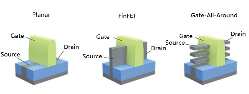
Figure 1: Structural Comparison of MOSFET, FinFET, and GAAFET
2. Atomic Layer Deposition
2.1. Technology Introduction
Atomic Layer Deposition (ALD) is a process developed for large-area thin film deposition with good uniformity, achieved through its fundamental self-limiting characteristics. As shown in Figure 2, a typical ALD surface chemical adsorption process for depositing Al₂O₃ films using Trimethylaluminum (Al(CH₃)₃, TMA) and water (H₂O) as precursors is as follows [3,4]:
(1) Pulse 1: The initial substrate surface is rich in -OH groups, which first react with the TMA vapor pulse. The -CH₃ groups in the TMA molecules exchange with the -OH groups on the surface, releasing CH₄ as a byproduct.
(2) Purge 1: Any remaining excess TMA and byproducts are removed by purging with an inert gas.
(3) Pulse 2: Next, H₂O vapor is introduced, which reacts with the adsorbed TMA surface species, replacing the -CH₃ groups with -OH groups on the substrate surface.
(4) Purge 2: Finally, any unreacted excess H₂O and byproducts are purged, and new -OH groups are formed on the surface.
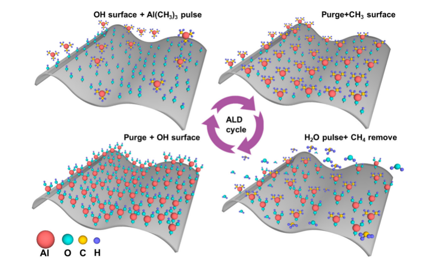
Figure 2: Schematic Diagram of the Basic Principles of ALD (using Trimethylaluminum (TMA) as the metal precursor and H₂O as the reactant).
ALD technology features self-limiting behavior [4], strong conformality, and high precision. Its growth rate is influenced by temperature effects and varies with reaction temperature, substrate surface reaction sites, reaction mechanisms, precursor polymerization, and thermal decomposition, with each ALD process having an “ALD process window” [5]. Currently, ALD technology faces two main challenges: thermal budget limitations and interface defect control. Conventional precursors exhibit poor reactivity at low temperatures, making it difficult to balance film quality and growth rate. During the deposition process, atomic-level impurities such as C and Cl can remain, introducing interface defects that severely affect the electrical performance of FET devices.
2.2. Impact on FET Device Characteristics
2.2.1. Optimization of Gate Dielectric Properties
As microelectronic devices continue to miniaturize, the ongoing reduction in size places stringent demands on the gate dielectric layer. Traditional silicon dioxide or silicon oxynitride gate dielectrics, when device sizes enter the submicron range, must have a thickness less than 1 nm to maintain constant gate capacitance and effective control over the channel. However, reducing thickness leads to severe issues, as direct tunneling current increases exponentially, which not only weakens the gate’s control over the channel but also significantly raises the power consumption of the device, severely hindering the advancement of microelectronics technology. High-k gate dielectrics, such as Al₂O₃ and HfO₂, fabricated using ALD technology, can increase the physical thickness of the gate dielectric layer due to their higher dielectric constants, effectively suppressing direct tunneling current and significantly reducing power consumption.
As an example, for an HfAlOx/Al₂O₃ bilayer high-k gate dielectric deposited using ALD technology: as shown in Figure 3, a diamond field-effect transistor (FET) with an HfAlOx/Al₂O₃ bilayer dielectric exhibits a gate leakage current density (|IGS|) of only 7.95×10⁻⁷ A/cm² at VGS = -6V, which is much lower than that of diamond FETs using traditional gate dielectrics such as MoO₃, LiF/Al₂O₃, Ta₂O₅/Al₂O₃, and ZrO₂/Al₂O₃ (with |IGS| values of 3.33×10⁻⁴ A/cm², 1×10⁻⁶ A/cm², 7.6×10⁻⁴ A/cm², and 4.8×10⁻⁵ A/cm², respectively). This reduction in leakage current leads to lower power consumption [6].
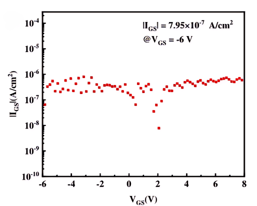
Figure 3: Gate Leakage Current Density (|IGS|) for a Diamond Field-Effect Transistor with an HfAlOx/Al₂O₃ Bilayer Dielectric.
2.2.2. Interface Optimization
At the interfaces of FET devices made from different materials, there are issues such as atomic interdiffusion, changes in interface chemical composition, and the formation of low-k interface layers. By introducing a specific passivation layer deposited using ALD technology at the material interfaces of transistors, interface defects can be reduced, interface state density lowered, charge trapping can be minimized, and carrier scattering reduced, thus maintaining interface stability and improving transistor performance.
For example, in the case of MOSFET candidate materials—Sm₂O₃/InP gate stacks: in this system, the leakage current density of the Sm₂O₃/Al₂O₃/InP stacked gate dielectric structure is lower than that of other samples. As shown in Figure 4(a), at room temperature, the leakage current density is 2.87×10⁻⁶ A/cm² at 1V. In Figure 4(b), at low temperatures (77-227K), the leakage current density of the Sm₂O₃/Al₂O₃/InP gate stack is nearly three orders of magnitude lower than at room temperature, with a value of 4.64×10⁻⁹ A/cm² at 77K [7].
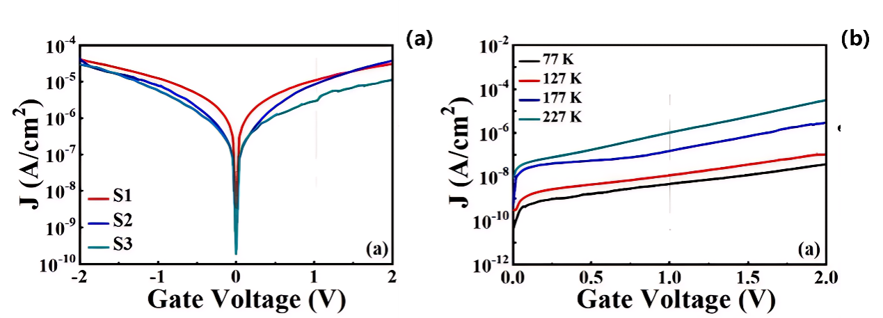
Figure 4: (a) J-V characteristics measured at room temperature; (b) J-V characteristics measured at low temperature.
Next, for WS₂ field-effect transistors (FETs), as shown in Figure 5(a), after introducing an Al₂O₃ passivation layer deposited by ALD, the carrier mobility significantly improves from an average of 9.4 cm² V⁻¹ s⁻¹ to 38 cm² V⁻¹ s⁻¹, and the range of mobility variation becomes smaller, with reduced impurity influence. As shown in Figure 5(b), in the WS₂ FET, the Al₂O₃ passivation layer protects the device from oxidation, maintaining stable electrical performance over 57 days. According to Figure 5(c), the WS₂ FET without Al₂O₃ passivation, after 19 days, shows a significant decrease in mobility from 6.5 cm² V⁻¹ s⁻¹ to 1.0 cm² V⁻¹ s⁻¹, indicating that the Al₂O₃ passivation layer significantly improves the environmental stability of the device [8].
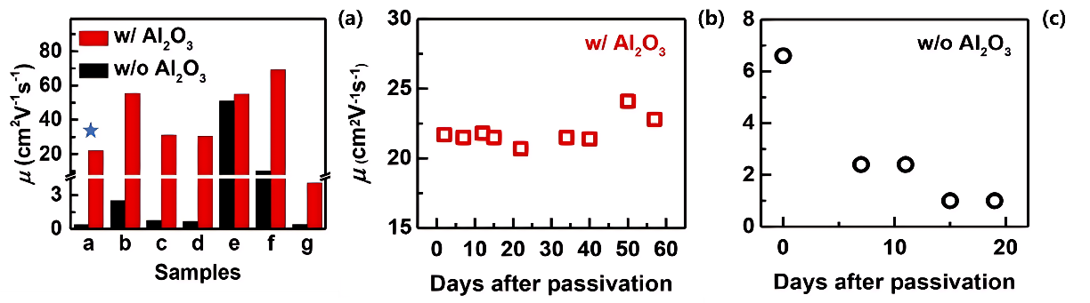
Figure 5: (a) Summary of mobility enhancement for seven WS₂ FETs labeled from a to g; (b) Relationship between extracted electron mobility of WS₂ transistors and time after Al₂O₃ passivation; (c) Extracted mobility of WS₂ transistor without passivation layer after 19 days.
3. Metal-Organic Chemical Vapor Deposition
3.1. Technology Introduction
Metal-Organic Chemical Vapor Deposition (MOCVD) is one of the key technologies for the preparation of semiconductor compound materials. This technique utilizes metal-organic compounds as source materials to gradually form thin films with specific structures and properties. Due to its ability to precisely control the film growth process, it plays an irreplaceable role in the preparation of high-quality, high-performance semiconductor compound materials, and is widely used in semiconductor and optoelectronic fields. As shown in Figure 6, the MOCVD process can be divided into the following steps [9]:
(1) Precursor Selection and Input: Suitable metal-organic precursors and reactive gases are selected. The precursor is usually a metal-organic compound containing the metal elements in the target film material, while the reactive gases are typically hydrogen, nitrogen, or other inert gases used as carrier gases.
(2) Gas Transport and Mixing: The precursor and reactive gases are mixed at the inlet of the reaction chamber, usually under controlled flow rates and pressures, ensuring uniform mixing of the gases, which are then introduced into the reaction chamber in the correct proportions.
(3) Deposition Reaction: The mixed gases flow onto a heated substrate, where the precursor decomposes and undergoes a chemical reaction on the substrate surface, generating the required solid material and depositing it onto the substrate.
(4) Exhaust of Byproducts and Unreacted Precursors: Any unreacted precursors and byproducts are carried away by the gas flow and expelled from the reaction chamber to avoid environmental contamination and ensure safety.
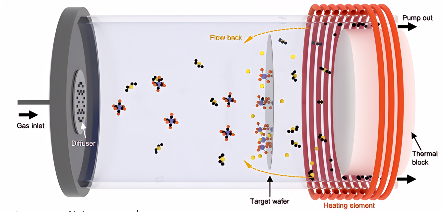
Figure 6: Schematic Diagram of the Basic Principles of MOCVD
MOCVD technology features broad material adaptability, high control precision, high material crystallization quality, strong scalability, and relatively high growth efficiency [10]. However, it also faces challenges such as difficulty in meeting purity requirements for raw materials, poor stability, unclear reaction mechanisms, and insufficient design of the reaction chamber structure. Its most significant drawback is the lack of real-time in situ monitoring technology for the growth process [10].
3.2. Impact on FET Device Characteristics
3.2.1. Reduction of Contact Resistance
MOCVD technology can reduce the contact resistance of FET devices by selecting special materials (such as two-dimensional materials or semi-metal materials), precisely controlling growth parameters (growth temperature, gas flow, and pressure, etc.), and designing special structures (heterostructures, multilayer structures). This not only improves carrier mobility, increases operating frequency and response speed, but also reduces power consumption, lowers heat generation, enhances energy efficiency, and improves the stability and reliability of the devices, reducing faults and lowering production costs. This significantly promotes the development of FET device applications across multiple fields.
For example, in the MOCVD-grown Al₀.₇Ga₀.₃N/Al₀.₅Ga₀.₅N heterojunction field-effect transistor, Figure 7(a) shows the I-V characteristics of two terminals with a contact spacing of 2.6 µm, indicating that the contact layer design of the fully grown MOFET exhibits good ohmic behavior. Figure 7(b) compares the reported contact resistivity (ρ) function for the AlGaN channel, previously discussed in AlGaN channel research [11]. The low contact resistance is due to the lack of Al composition mismatch during the MOCVD growth process, as both the contact layer and heterostructure are completed in a single growth process, with optimized plasma treatment and metallization processes, better controlling the Al composition.
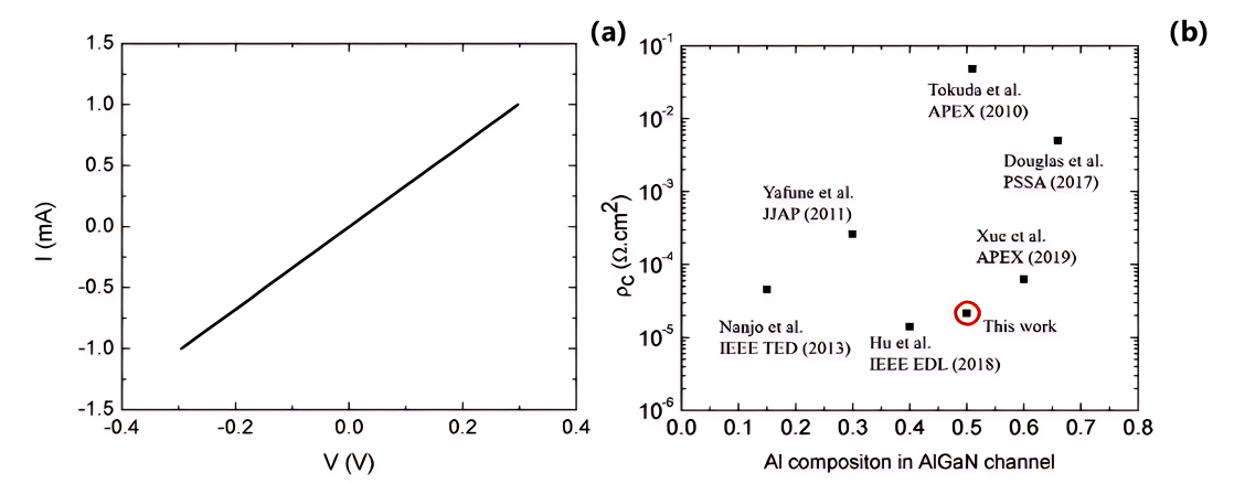
Figure 7: (a) I-V characteristics of two terminals with a contact spacing of 2.6 µm; (b) Comparison of reported specific contact resistivity (ρ) for the AlGaN channel.
Moreover, studies have shown that Si-doped (010) β-Ga₂O₃ grown using MOCVD technology, along with its epitaxial material, has achieved record-high electron mobility. At room temperature, the thin film with a doping concentration of 2.5×10⁻¹⁶ cm³ exhibits a carrier mobility of 184 cm²/Vs. At 45K low temperature, with a doping concentration of 2.75×10⁻¹⁶ cm³, the carrier mobility increases to 4984 cm²/Vs [12]. If used to fabricate FET devices, this material is expected to reduce contact resistance.
3.2.2. Enhancement of Breakdown Voltage
MOCVD technology can optimize FET device structures, improve electric field distribution, reduce the electric field strength in high-field regions, and prevent premature breakdown. Furthermore, the flexibility of MOCVD allows for the growth of multilayer structures, optimizing electric field distribution, such as in superjunction FET structures. It can also grow graded material layers, mitigating heterojunction interface stress and overall enhancing the breakdown voltage of FET devices.
For example, in the case of MOCVD-grown n-type GaN epitaxial layers on miscut sapphire substrates, the graded and doped AlGaN back barrier induces the formation of a two-dimensional electron gas (2DEG) channel, which confines electrons in the 2DEG channel and reduces electron injection into the buffer, thereby isolating the buffer region from the channel and reducing dispersion effects caused by buffer traps. At the same time, the top AlGaN layer helps reduce gate leakage, enabling a higher breakdown voltage. As shown in Figure 8, the device’s breakdown voltage exceeds 2000V, and compared to the nominal LGD=18 µm device (VBR = 1900V), the device with the epitaxial layer structure and LGD=28 µm exhibits an even higher breakdown voltage [13].
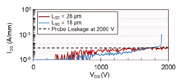
Figure 8: Drain current (leakage) as a function of drain voltage in the off state (VGS = -9V).
4. Pulsed Laser Deposition
4.1. Technology Introduction
Pulsed Laser Deposition (PLD) is a type of physical vapor deposition (PVD) method. It uses the energy of pulsed lasers to bombard a target material, causing it to vaporize and form a plasma. This plasma then deposits onto a substrate and self-assembles into a thin film. As shown in Figure 9, when preparing thin films using pulsed laser deposition, PLD technology can be divided into three stages [14,15]:
(1) Laser-Target Interaction: High-energy pulsed lasers are focused on the target material. Due to the short duration of the pulses and the concentrated energy, the target material absorbs heat rapidly. The surface temperature rises sharply, causing the material to overcome bonding forces, evaporate, melt, and ionize, forming a high-temperature, high-density plasma cloud containing various particles. The properties of the target material and the characteristics of the laser affect this process.
(2) Plasma Expansion: In the plasma, particles collide and ionize, maintaining high temperature and pressure. Due to the pressure difference between the inside and outside, the plasma expands along the direction of the laser incident normal, causing a decrease in temperature and density. If there is background gas, particles will collide with it, altering their motion and energy.
(3) Film Growth: The plasma particles are deposited onto the substrate, initially adsorbing randomly. After reaching a certain amount, the particles aggregate to form nuclei. The state and temperature of the substrate affect the formation of these nuclei. The nuclei adsorb particles, grow, and connect, ultimately forming a continuous thin film.
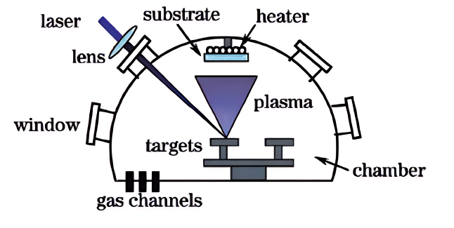
Figure 9: Schematic of the Basic Principles of PDL.
PLD technology has several advantages in preparing high-quality thin films, including strong deposition compositional integrity, controllable structure and morphology, a wide range of materials that can be prepared, and high deposition efficiency (up to 10 µm/min) [16]. However, it also faces issues such as poor thickness uniformity, roughening of the target surface, and significant compositional loss variations.
4.2. Impact on FET Device Characteristics
4.2.1. Improvement of Switching Ratio
In FET devices, PLD technology can improve the switching ratio by optimizing the structure of semiconductor materials and the distribution of impurities. The switching ratio significantly influences the performance of FET devices: under a high switching ratio, in the “on” state, the FET behaves like a good conductor, efficiently transmitting current to meet the circuit’s signal and power requirements. In the “off” state, it is almost an insulator, greatly reducing leakage current and static power consumption. With respect to frequency response, a high switching ratio enables the device to quickly switch between the “on” and “off” states, reducing high-frequency signal distortion and improving high-frequency performance.
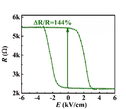
Figure 10: The variation of resistance with electric field for In₂O₃ films deposited at 2 Pa and 600°C by PLD.
As shown in Figure 10, when a series of In₂O₃ semiconductor thin films are grown on ferroelectric single-crystal substrates using PLD technology to form ferroelectric field-effect transistor devices, the highest switching ratio (DR/R) of the PLD-deposited In₂O₃ thin film reaches 144% at 2 Pa and 600°C [17], which is larger than the switching ratios of previously reported structures such as La₂/₃Ba₁/₃MnO₃/PMN–PT [18], ZnO/PMN-PT [19], and TiO₂-d/PMN–PT [20].
Furthermore, studies have shown that BP thin films grown using PLD technology exhibit excellent electrical properties in terms of field-effect mobility (μFE) and current switching ratio. As shown in Figure 11, at a thickness of 5 nm, the field-effect transistor based on this thin film exhibits relatively good overall electrical performance. The carrier mobility is high, reaching 213 and 617 cm²/V·s at 295 K and 250 K, respectively [21].
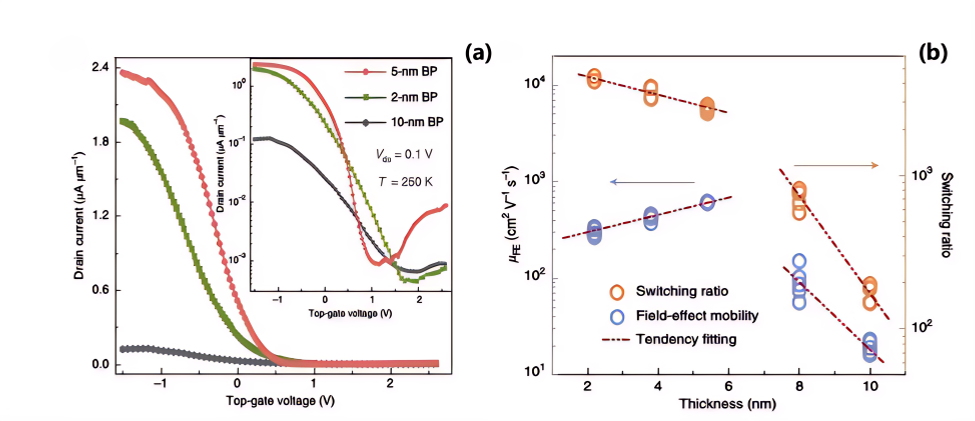
Figure 11: (a) Transfer characteristics of field-effect transistors based on 2 nm, 5 nm, and 10 nm BP ultra-thin films at 250K under linear scaling. (b) Variation of field-effect mobility (μFE) and switching ratio with BP film thickness based on repeated experiments.
4.2.2. Enhanced Photosensitivity
PLD technology allows for the control of laser pulse parameters such as the number of pulses, energy density, and frequency. An increase in pulse number and energy density results in thicker films, where more material participates in light absorption, generating more photogenerated carriers and thus enhancing photosensitivity. Rapid changes in photocurrent allow for the quick detection and response to light signals, making it suitable for high-speed optoelectronic devices such as optical communication systems and optical switches, improving the performance and application value of field-effect transistors in optoelectronic devices.
Taking MoS₂ thin films deposited by PLD as an example, the back-gate field-effect transistors made from these films have great application potential in photodetectors due to their unique bandgap. The transfer characteristic curves under illumination and in the dark are compared in Figure 12(a), showing that under illumination, the Ids transfer characteristic curve of the sample is higher than that under dark conditions. As shown in Figure 12(b), with the increase in illumination light power, the current increases significantly. When the source-drain voltage (Vds) is -1V and -2V, a linear relationship between light intensity and current can be observed (see Figure 12b insert). These results indicate that MoS₂ generates photogenerated carriers under light, and MoS₂ back-gate field-effect transistors exhibit good photosensitive performance [22].
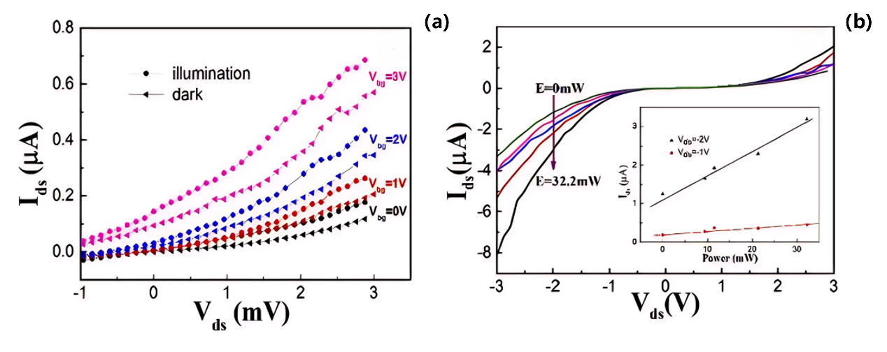
Figure 12: (a) I-V characteristics of MoS₂ FETs under dark and illuminated conditions at different back-gate voltages. (b) I-V characteristics of MoS₂ FETs under different light power levels (from 0 mW to 32.2 mW) at Vg = 0V.
5. Conclusion and Outlook
This paper discusses new preparation processes for field-effect transistors (FETs): Atomic Layer Deposition (ALD), Metal-Organic Chemical Vapor Deposition (MOCVD), and Pulsed Laser Deposition (PLD). ALD can optimize gate dielectric properties and reduce interface defects; MOCVD can reduce contact resistance and improve breakdown voltage; PLD can enhance switching ratio and photosensitivity. All three technologies significantly optimize FET device characteristics. However, each of these processes faces technical challenges: ALD’s thermal budget limitations lead to insufficient reaction activity of conventional precursors at low temperatures, and the deposition process tends to leave impurities that form interface defects; MOCVD suffers from poor raw material purity and stability, unclear reaction mechanisms, and a lack of real-time in situ monitoring of the growth process; PLD encounters issues such as poor film thickness uniformity, target surface roughening, and large compositional loss variations. Future efforts could focus on optimizing process conditions, combining multiple processes for synergistic treatment, and further exploring the potential of these new technologies to drive continuous innovation and development of FET devices in the semiconductor field, meeting the growing demand for high performance.
References
[1]. Duan, H. (2024). From MOSFET to FinFET to GAAFET: The evolution, challenges, and future prospects. Applied and Computational Engineering, 50(1), 113-120. https://doi.org/10.54254/2755-2721/50/20241285
[2]. Zhang, S. (2020). Review of modern field effect transistor technologies for scaling. Journal of Physics: Conference Series, 1617(1), 012054. https://doi.org/10.1088/1742-6596/1617/1/012054
[3]. Sheng, J., Lee, J. H., Choi, W. H., et al. (2018). Review article: Atomic layer deposition for oxide semiconductor thin film transistors: Advances in research and development. Journal of Vacuum Science & Technology A: Vacuum, Surfaces, and Films, 36(6), 060801. https://doi.org/10.1116/1.5047237
[4]. Johnson, R. W., Hultqvist, A., & Bent, S. F. (2014). A brief review of atomic layer deposition: From fundamentals to applications. Materials Today, 17(5), 236-246. https://doi.org/10.1016/j.mattod.2014.04.026
[5]. Lu, J., Elam, J. W., & Stair, P. C. (2016). Atomic layer deposition—Sequential self-limiting surface reactions for advanced catalyst “bottom-up” synthesis. Surface Science Reports, 71(2), 410-472. https://doi.org/10.1016/j.surfrep.2016.03.003
[6]. Zhang, M., Lin, F., Wang, W., et al. (2022). HfAlOx/Al2O3 bilayer dielectrics for a field effect transistor on a hydrogen-terminated diamond. Materials, 15(2), 446. https://doi.org/10.3390/ma15020446
[7]. Lu, J., He, G., Yan, J., et al. (2021). Interface optimization and transport modulation of Sm2O3/InP metal oxide semiconductor capacitors with atomic layer deposition-derived laminated interlayer. Nanomaterials, 11(12), 3443. https://doi.org/10.3390/nano11123443
[8]. You, Y. G., Shin, D. H., Ryu, J. H., et al. (2021). Atomic layer deposited Al2O3 passivation layer for few-layer WS2 field effect transistors. Nanotechnology, 32(50), 505702. https://doi.org/10.1088/1361-6528/ac2390
[9]. Zhu, J., Park, J. H., & Vitale, S. A. (2023). Low-thermal-budget synthesis of monolayer molybdenum disulfide for silicon back-end-of-line integration on 200 mm platform. Nature Nanotechnology, 18(5), 456-+. https://doi.org/10.1038/s41565-023-01375-6
[10]. Tadjer, M. J., Alema, F., Osinsky, A., et al. (2024). Characterization of Ga2O3 homoepitaxial films and MOSFETs grown by MOCVD at high growth rates. Vacuum, 61(4), 102-104. https://doi.org/10.13385/j.cnki.vacuum.2024.04.19
[11]. Zhang, Y. C. (2020). Lecture 22: Chemical vapor deposition (CVD) technology. Solid-State Electronics, 164, 107696. https://doi.org/10.1016/j.sse.2019.107696
[12]. Xue, H., Hwang, S., Razzak, T., et al. (2019). All MOCVD grown Al0.7Ga0.3N/Al0.5Ga0.5N HFET: An approach to make ohmic contacts to Al-rich AlGaN channel transistors. Applied Physics Letters, 114(25), 250601. https://doi.org/10.1063/1.5109678
[13]. Feng, Z., Anhar Uddin Bhuiyan, A. F. M., Karim, M. R., et al. (2020). MOCVD homoepitaxy of Si-doped (010) β-Ga2O3 thin films with superior transport properties. Semiconductor Science and Technology, 35(12), 124004. https://doi.org/10.1088/1361-6641/abbfeb
[14]. Koksaldi, O. S., Romanczyk, B., Haller, J., et al. (2023). High-electron-mobility transistors with metal-organic chemical vapor deposition-regrown contacts for high voltage applications. Chemical Society Reviews, 52(7), 2294-2321. https://doi.org/10.1039/D2CS00938B
[15]. Deng, Z., Jia, Q., Feng, B., et al. (2021). Research progress on fabrication and applications of high-performance films by pulsed laser deposition. Chinese Journal of Lasers, 48(8), 0802010. https://doi.org/10.3788/CJL202148.0802010
[16]. Feng, B., Shen, D., Wang, W., et al. (2019). Cooperative bilayer of lattice-disordered nanoparticles as room-temperature sinterable nanoarchitecture for device integrations. ACS Applied Materials & Interfaces, 11(18), 16972-16980. https://doi.org/10.1021/acsami.9b00307
[17]. Xu, M., Guo, L., Yan, J. M., et al. (2021). Optimization of the pulsed laser deposition process of In2O3 thin films for ferroelectric field effect device applications. Journal of Materials Science: Materials in Electronics, 32(2), 1659-1667. https://doi.org/10.1007/s10854-020-04935-x
[18]. Zhao, W., Huang, W., Liu, C., et al. (2021). Electric-field-controlled nonvolatile magnetization rotation and magnetoresistance effect in Co/Cu/Ni spin valves on piezoelectric substrates. ACS Applied Materials & Interfaces, 11(18), 16972-16980. https://doi.org/10.1021/acsami.8b03761
[19]. Malashevich, A., Marshall, M. S. J., Visani, C., et al. (2018). Controlling mobility in perovskite oxides by ferroelectric modulation of atomic-scale interface structure. Nano Letters, 18(1), 573-578. https://doi.org/10.1021/acs.nanolett.7b04715
[20]. Yan, J. M., Xu, Z. X., Chen, T. W., et al. (2021). Nonvolatile and reversible ferroelectric control of electronic properties of Bi2Te3 topological insulator thin films grown on Pb(Mg1/3Nb2/3)O3-PbTiO3 single crystals. ACS Applied Materials & Interfaces, 11(18), 16972-16980. https://doi.org/10.1021/acsami.8b20406
[21]. Wu, Z., Lyu, Y., Zhang, Y., et al. (2021). Large-scale growth of few-layer two-dimensional black phosphorus. Nature Materials, 20(9), 1203-1209. https://doi.org/10.1038/s41563-021-01001-7
[22]. Xi, J., Huang, X., Hu, M., et al. (2020). Dependence of laser parameters on structural properties of pulsed laser-deposited MoS2 thin films applicable for field effect transistors. Journal of Materials Science: Materials in Electronics, 31(23), 21118-21127. https://doi.org/10.1007/s10854-020-04624-9
Cite this article
Ding,H. (2025). The Impact of Novel Semiconductor Manufacturing Processes on Field Effect Transistor Characteristics. Applied and Computational Engineering,142,64-73.
Data availability
The datasets used and/or analyzed during the current study will be available from the authors upon reasonable request.
Disclaimer/Publisher's Note
The statements, opinions and data contained in all publications are solely those of the individual author(s) and contributor(s) and not of EWA Publishing and/or the editor(s). EWA Publishing and/or the editor(s) disclaim responsibility for any injury to people or property resulting from any ideas, methods, instructions or products referred to in the content.
About volume
Volume title: Proceedings of MSS 2025 Symposium: Automation and Smart Technologies in Petroleum Engineering
© 2024 by the author(s). Licensee EWA Publishing, Oxford, UK. This article is an open access article distributed under the terms and
conditions of the Creative Commons Attribution (CC BY) license. Authors who
publish this series agree to the following terms:
1. Authors retain copyright and grant the series right of first publication with the work simultaneously licensed under a Creative Commons
Attribution License that allows others to share the work with an acknowledgment of the work's authorship and initial publication in this
series.
2. Authors are able to enter into separate, additional contractual arrangements for the non-exclusive distribution of the series's published
version of the work (e.g., post it to an institutional repository or publish it in a book), with an acknowledgment of its initial
publication in this series.
3. Authors are permitted and encouraged to post their work online (e.g., in institutional repositories or on their website) prior to and
during the submission process, as it can lead to productive exchanges, as well as earlier and greater citation of published work (See
Open access policy for details).
References
[1]. Duan, H. (2024). From MOSFET to FinFET to GAAFET: The evolution, challenges, and future prospects. Applied and Computational Engineering, 50(1), 113-120. https://doi.org/10.54254/2755-2721/50/20241285
[2]. Zhang, S. (2020). Review of modern field effect transistor technologies for scaling. Journal of Physics: Conference Series, 1617(1), 012054. https://doi.org/10.1088/1742-6596/1617/1/012054
[3]. Sheng, J., Lee, J. H., Choi, W. H., et al. (2018). Review article: Atomic layer deposition for oxide semiconductor thin film transistors: Advances in research and development. Journal of Vacuum Science & Technology A: Vacuum, Surfaces, and Films, 36(6), 060801. https://doi.org/10.1116/1.5047237
[4]. Johnson, R. W., Hultqvist, A., & Bent, S. F. (2014). A brief review of atomic layer deposition: From fundamentals to applications. Materials Today, 17(5), 236-246. https://doi.org/10.1016/j.mattod.2014.04.026
[5]. Lu, J., Elam, J. W., & Stair, P. C. (2016). Atomic layer deposition—Sequential self-limiting surface reactions for advanced catalyst “bottom-up” synthesis. Surface Science Reports, 71(2), 410-472. https://doi.org/10.1016/j.surfrep.2016.03.003
[6]. Zhang, M., Lin, F., Wang, W., et al. (2022). HfAlOx/Al2O3 bilayer dielectrics for a field effect transistor on a hydrogen-terminated diamond. Materials, 15(2), 446. https://doi.org/10.3390/ma15020446
[7]. Lu, J., He, G., Yan, J., et al. (2021). Interface optimization and transport modulation of Sm2O3/InP metal oxide semiconductor capacitors with atomic layer deposition-derived laminated interlayer. Nanomaterials, 11(12), 3443. https://doi.org/10.3390/nano11123443
[8]. You, Y. G., Shin, D. H., Ryu, J. H., et al. (2021). Atomic layer deposited Al2O3 passivation layer for few-layer WS2 field effect transistors. Nanotechnology, 32(50), 505702. https://doi.org/10.1088/1361-6528/ac2390
[9]. Zhu, J., Park, J. H., & Vitale, S. A. (2023). Low-thermal-budget synthesis of monolayer molybdenum disulfide for silicon back-end-of-line integration on 200 mm platform. Nature Nanotechnology, 18(5), 456-+. https://doi.org/10.1038/s41565-023-01375-6
[10]. Tadjer, M. J., Alema, F., Osinsky, A., et al. (2024). Characterization of Ga2O3 homoepitaxial films and MOSFETs grown by MOCVD at high growth rates. Vacuum, 61(4), 102-104. https://doi.org/10.13385/j.cnki.vacuum.2024.04.19
[11]. Zhang, Y. C. (2020). Lecture 22: Chemical vapor deposition (CVD) technology. Solid-State Electronics, 164, 107696. https://doi.org/10.1016/j.sse.2019.107696
[12]. Xue, H., Hwang, S., Razzak, T., et al. (2019). All MOCVD grown Al0.7Ga0.3N/Al0.5Ga0.5N HFET: An approach to make ohmic contacts to Al-rich AlGaN channel transistors. Applied Physics Letters, 114(25), 250601. https://doi.org/10.1063/1.5109678
[13]. Feng, Z., Anhar Uddin Bhuiyan, A. F. M., Karim, M. R., et al. (2020). MOCVD homoepitaxy of Si-doped (010) β-Ga2O3 thin films with superior transport properties. Semiconductor Science and Technology, 35(12), 124004. https://doi.org/10.1088/1361-6641/abbfeb
[14]. Koksaldi, O. S., Romanczyk, B., Haller, J., et al. (2023). High-electron-mobility transistors with metal-organic chemical vapor deposition-regrown contacts for high voltage applications. Chemical Society Reviews, 52(7), 2294-2321. https://doi.org/10.1039/D2CS00938B
[15]. Deng, Z., Jia, Q., Feng, B., et al. (2021). Research progress on fabrication and applications of high-performance films by pulsed laser deposition. Chinese Journal of Lasers, 48(8), 0802010. https://doi.org/10.3788/CJL202148.0802010
[16]. Feng, B., Shen, D., Wang, W., et al. (2019). Cooperative bilayer of lattice-disordered nanoparticles as room-temperature sinterable nanoarchitecture for device integrations. ACS Applied Materials & Interfaces, 11(18), 16972-16980. https://doi.org/10.1021/acsami.9b00307
[17]. Xu, M., Guo, L., Yan, J. M., et al. (2021). Optimization of the pulsed laser deposition process of In2O3 thin films for ferroelectric field effect device applications. Journal of Materials Science: Materials in Electronics, 32(2), 1659-1667. https://doi.org/10.1007/s10854-020-04935-x
[18]. Zhao, W., Huang, W., Liu, C., et al. (2021). Electric-field-controlled nonvolatile magnetization rotation and magnetoresistance effect in Co/Cu/Ni spin valves on piezoelectric substrates. ACS Applied Materials & Interfaces, 11(18), 16972-16980. https://doi.org/10.1021/acsami.8b03761
[19]. Malashevich, A., Marshall, M. S. J., Visani, C., et al. (2018). Controlling mobility in perovskite oxides by ferroelectric modulation of atomic-scale interface structure. Nano Letters, 18(1), 573-578. https://doi.org/10.1021/acs.nanolett.7b04715
[20]. Yan, J. M., Xu, Z. X., Chen, T. W., et al. (2021). Nonvolatile and reversible ferroelectric control of electronic properties of Bi2Te3 topological insulator thin films grown on Pb(Mg1/3Nb2/3)O3-PbTiO3 single crystals. ACS Applied Materials & Interfaces, 11(18), 16972-16980. https://doi.org/10.1021/acsami.8b20406
[21]. Wu, Z., Lyu, Y., Zhang, Y., et al. (2021). Large-scale growth of few-layer two-dimensional black phosphorus. Nature Materials, 20(9), 1203-1209. https://doi.org/10.1038/s41563-021-01001-7
[22]. Xi, J., Huang, X., Hu, M., et al. (2020). Dependence of laser parameters on structural properties of pulsed laser-deposited MoS2 thin films applicable for field effect transistors. Journal of Materials Science: Materials in Electronics, 31(23), 21118-21127. https://doi.org/10.1007/s10854-020-04624-9