


1. Introduction
In the design of analog integrated circuits, the folded cascode operational amplifier has become one of the core modules for low-voltage, high-precision applications due to its high gain, wide output swing, and excellent power supply voltage adaptability. As CMOS technology advances to the nanometer scale, the power supply voltage continues to decrease, and issues such as limited output swing and increased noise sensitivity of traditional common-source cascode structures have become more pronounced, posing greater challenges for the design of high-gain operational amplifiers.
This paper focuses on the optimization design of folded cascode operational amplifiers. By introducing dynamic biasing techniques and noise suppression strategies, the design improves both DC gain and bandwidth while meeting the demands for low power consumption and high linearity. In recent years, scholars have conducted several innovative studies on folded cascode structures: Xiao Ben et al. [1] used adaptive compensation technology based on the 28 nm CMOS process to achieve a gain of 78 dB and a bandwidth of 5.2 MHz, with a power consumption of only 1.8 mW; Wang Jiaqi et al. [2] incorporated chopping stabilization technology into the folded cascode structure, increasing the common-mode rejection ratio (CMRR) to 110 dB; Li Xin et al. [3] improved current matching at the folding node to achieve a gain of 65 dB and a slew rate of 3.5 V/μs under a 0.8 V supply, significantly expanding the low-voltage application scenarios. However, existing solutions still have limitations in the collaborative optimization of gain and bandwidth, as well as process robustness. This paper optimizes the folded cascode input stage and employs Miller compensation to enhance both DC gain and CMRR while addressing the need for low power consumption and stability.
2. Circuit design
The input stage of the operational amplifier proposed in this paper is shown in Figure 1. To improve the suppression of common-mode noise, differential inputs are necessary. At the same time, to ensure that the input stage introduces minimal noise, PMOS transistors were chosen as the input transistors, with PM5 serving as the load current source to provide bias current. The current of PM7 and PM8 flows through NM0 and NM1, entering the common-source cascode load transistors PM0, PM1, PM11, and PM12, where it is converted to a voltage output to the next stage of the circuit.
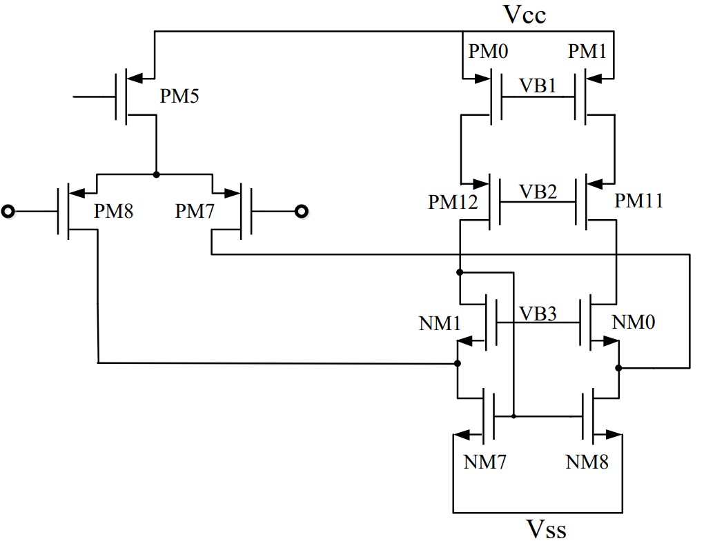
Figure 1: Input stage of the operational amplifier
The complete operational amplifier circuit proposed in this paper is shown in Figure 2. PM2, PM3, NM2, NM3, and resistors form the current biasing circuit, generating a bias current of 40 μA, which is then copied to other branches through PM4 and NM4. PM7 and PM8 form the differential input transistors, with PM5 acting as the tail current source, setting the tail current to 80 μA, providing 40 μA of working current to each of the input transistors. The current mirror formed by PM0 and PM1 also copies the 40 μA current, and with the current flowing through the input transistors, the working current of NM7 and NM8 is 80 μA.
PM6 and NM5 form the voltage biasing circuit, providing bias for NM1 and NM6. PM9 and NM0 provide bias for PM11 and PM12. Therefore, NM5 and PM9 are connected in a diode configuration. Considering the power consumption limitations, the width-to-length ratio of PM6 and NM0 is set small, and they only copy small currents to form the bias circuit. The bias for NM7 and NM8 is provided by the drain voltage of NM1, which reduces the number of bias circuits and, therefore, reduces power consumption.
The second-stage amplifier consists of a common-source amplifier formed by PM10 and NM9. Considering the output driving capability of the amplifier, the current for the second-stage amplifier is designed to be 400 μA. This is because the second-stage amplifier needs to provide a large gain and a fast transition rate. Therefore, a larger current is copied, and NM9 needs to provide a larger gain, so its width-to-length ratio is also larger. To account for small size effects and the impact of PVT (Process-Voltage-Temperature) variations on circuit performance, the channel length of the transistors in this stage cannot be too small. After considering all factors, the channel length is set to 1 μm.
Figure 2: Complete operational amplifier circuit proposed in this paper
3. Simulation results
The simulations in this paper were carried out using the Spectre simulator in Cadence software. With a 1.8V supply voltage, DC gain, phase margin, common-mode rejection ratio (CMRR), power supply rejection ratio (PSRR), and slew rate were simulated at five process corners: TT, SS, FF, SNFP, and FNSP, under temperatures of -40°C, 25°C, and 125°C. The simulation results indicate that the circuit exhibits good robustness under the TT, SS, FF, SF, and FS process corners when the temperature ranges from -45°C to 125°C.
The simulation data for DC gain and phase margin are shown in Figures 3 and 4. During the temperature variation from -40°C to 125°C, the open-loop DC gain at different process corners is greater than 84dB, and the phase margin is approximately 70°.
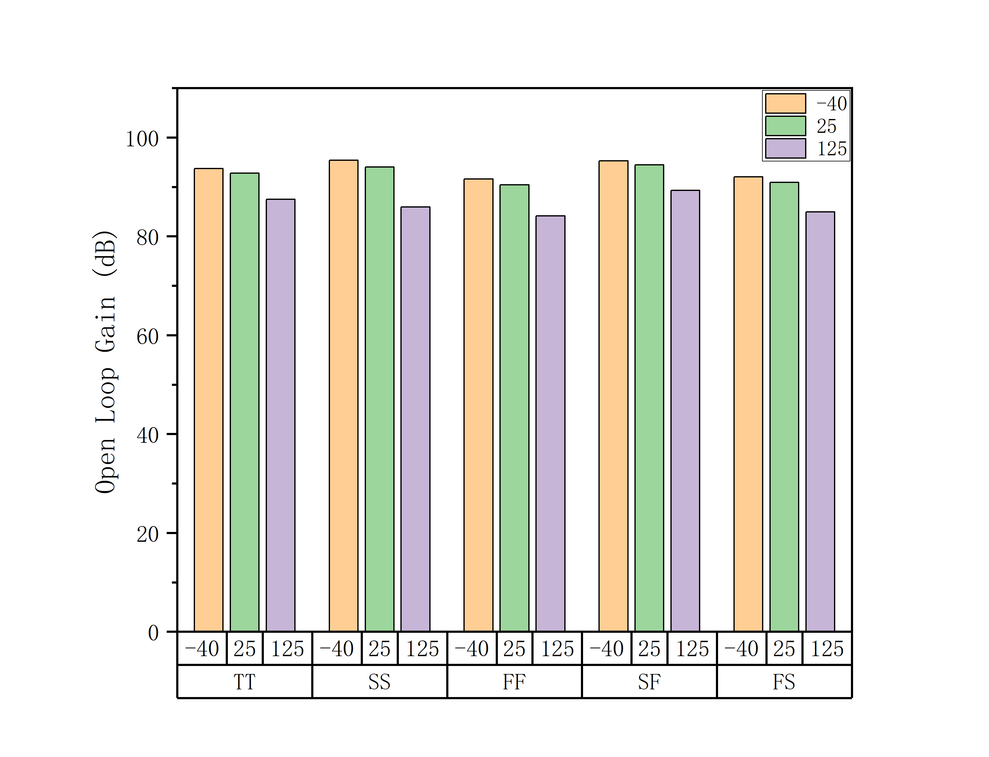
Figure 3: DC gain simulation data
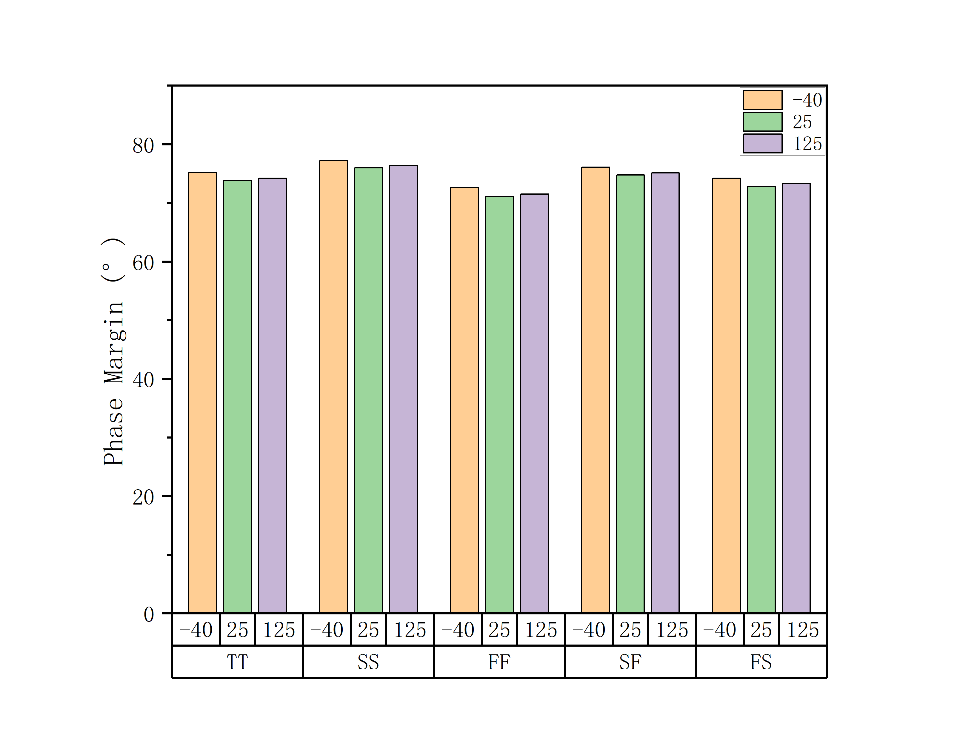
Figure 4: Phase margin simulation data
The simulation data for the common-mode rejection ratio (CMRR) is shown in Figure 5. Under the varying temperature range from -40°C to 125°C, the CMRR at different process corners is greater than 130dB.
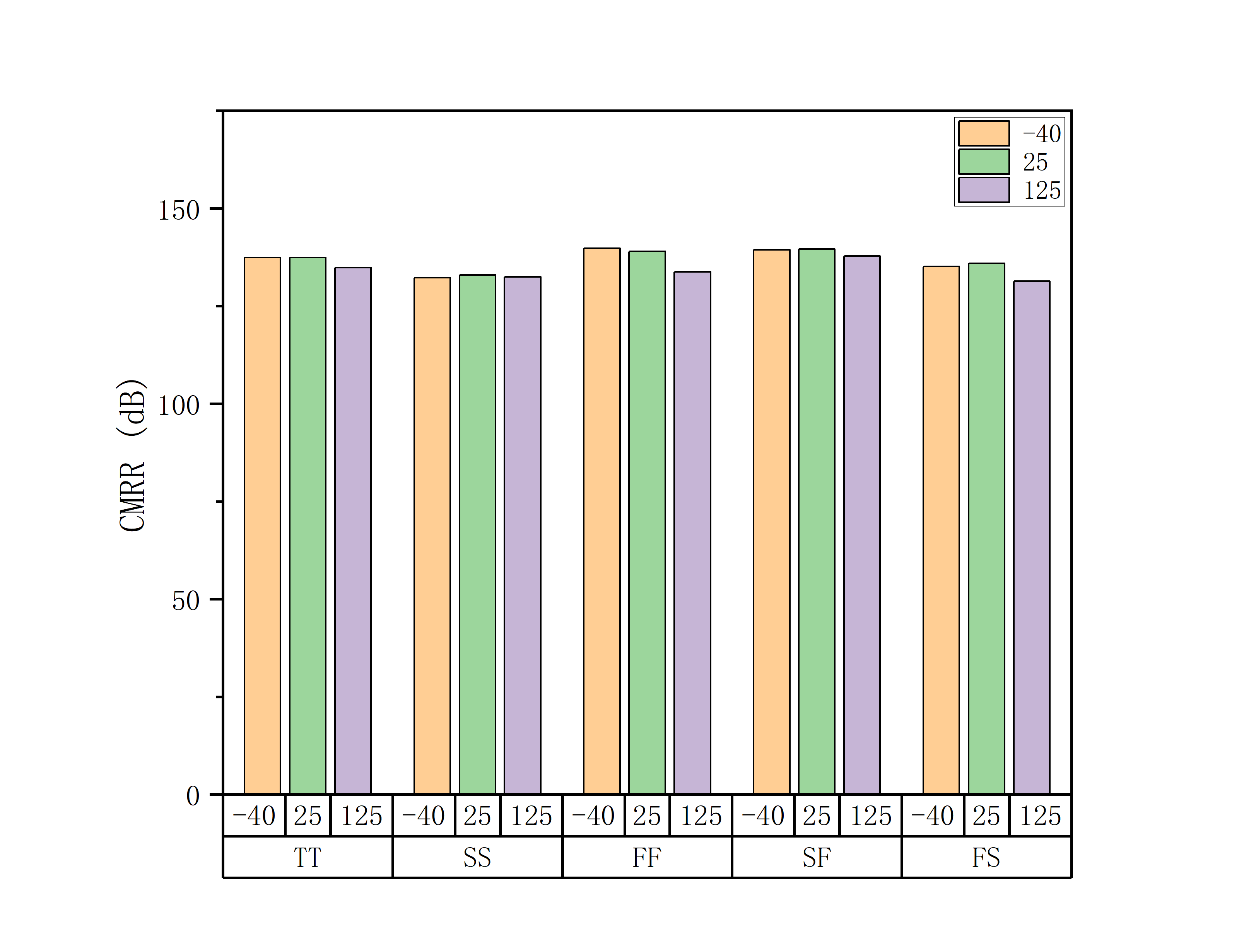
Figure 5: Common-mode rejection ratio simulation data
The simulation data for the power supply rejection ratio (PSRR) is shown in Figure 6. During the temperature variation from -40°C to 125°C at different process corners, the negative power supply rejection ratio is greater than 114dB.
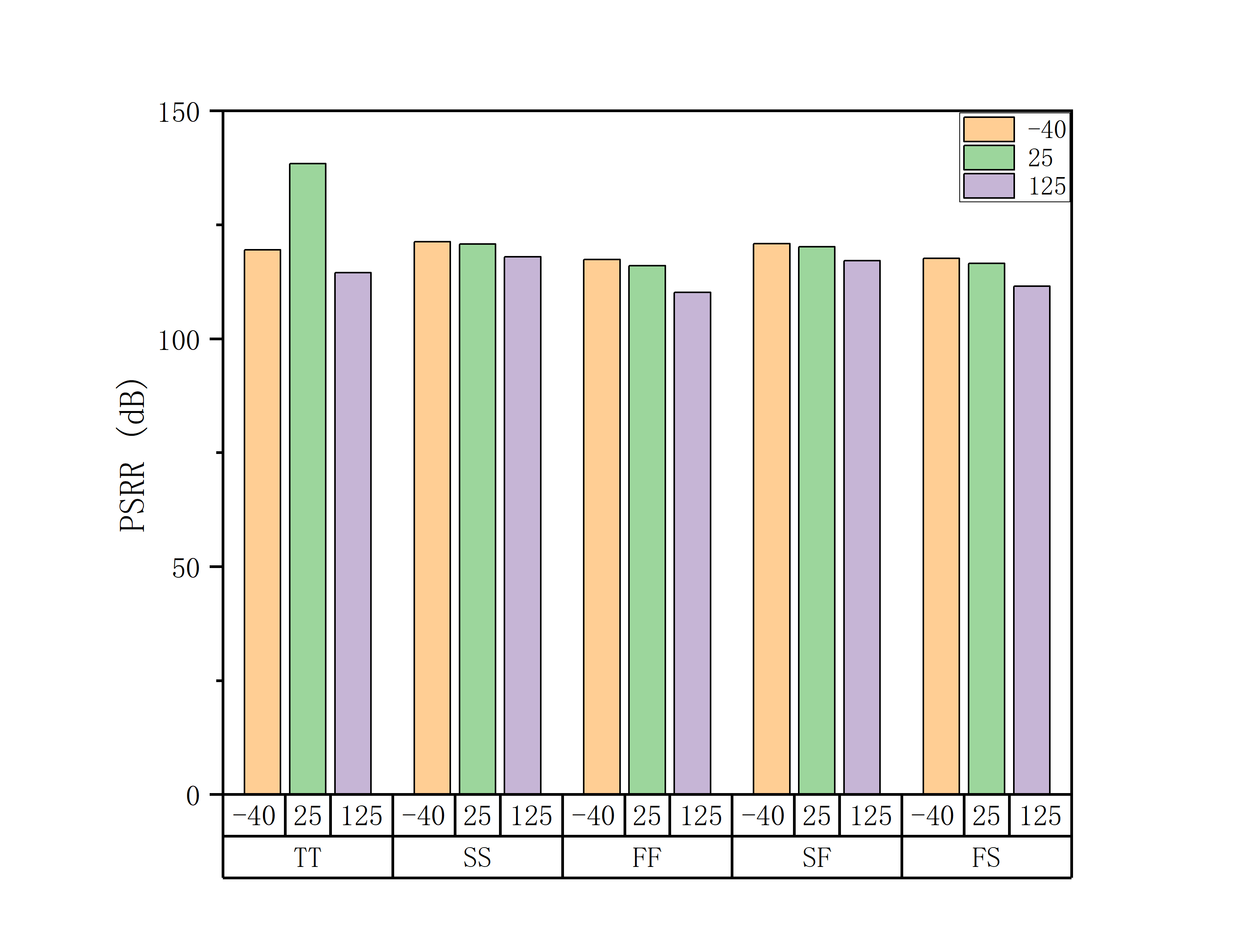
Figure 6: Negative power supply rejection ratio simulation data
The simulation data for the slew rate is shown in Figure 7. During the temperature variation from -40°C to 125°C at different process corners, the slew rate varies within the range of [54 V/μs, 74 V/μs].
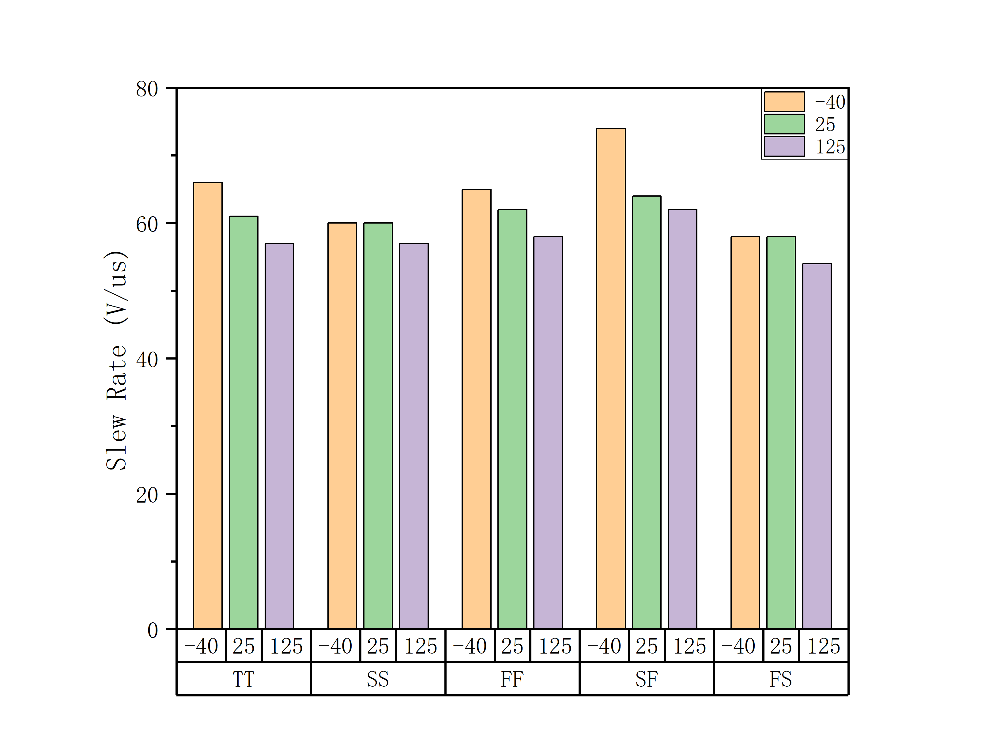
Figure 7: Slew rate simulation data
The comparison between this work and recent works in other papers is shown in Table 1. Literature [5] reports an operational amplifier designed using an advanced process that has significant advantages in power consumption, but it is also constrained by process limitations, failing to achieve better performance in terms of DC gain and slew rate.
Table 1: Comparison between this work and other papers
Index | This article | Document [4] | Document [5] |
Process | TSMC 180nm | 180nm | 28nm |
Supply voltage | 1.8V | 1.8V | 1.8V |
Load capacitor | 2pF | 2pF | 1pF |
Zero-frequency gain | >84dB | 117.36dB | 96dB |
Phase margin | 70° | 70° | 63° |
CMRR | >130dB | 109.41dB | NA |
PSRR | >114dB | NA | 86.7dB |
Slew rate | >54V/us | 40.21V/us | 33V/us |
Power dissipation | 1.5mW@tt25℃ | 1.37mW | 0.142mW |
From the above data, it can be seen that compared to existing operational amplifiers both domestically and internationally, the gain is intermediate, meeting medium precision requirements. The phase margin of 70° strikes a balance between stability and response speed, outperforming traditional two-stage amplifiers. The common-mode rejection ratio (CMRR) is significantly better than the reference specifications, reflecting the effectiveness of the common-mode feedback path design and optimization of the tail current source matching. The design in this paper performs excellently in terms of CMRR and power supply rejection ratio (PSRR), making it suitable for signal conditioning circuits in high-noise environments. Compared to similar domestic and international studies, its advantages lie in the suppression ratios and robustness, although there is considerable room for improvement in gain and power consumption.
4. Conclusion
This paper designs a two-stage fold-cascode operational amplifier. The first stage uses a folded common-source common-gate amplification structure, while the second stage employs a common-source amplifier structure. The design utilizes methods such as Miller compensation to ensure the frequency characteristics of the two-stage amplifier meet stability requirements. The operational amplifier circuit was simulated and verified under different process corners and temperatures. The simulation results show that its open-loop DC gain is greater than 84dB, the phase margin is approximately 70°, the common-mode rejection ratio is greater than 130dB, the negative power supply rejection ratio is greater than 114dB, and the static power consumption at room temperature is below 1.5mW, demonstrating good robustness. The first-stage folded common-source common-gate structure increases the output impedance by stacking transistors, contributing the main gain and providing the amplifier with a high open-loop amplification capability. Additionally, it exhibits excellent suppression of negative power supply noise and strong rejection of common-mode interference (such as power supply noise and environmental disturbances). Therefore, this structure is suitable for multi-supply systems or noise-sensitive environments, making it ideal for high-precision closed-loop applications.
References
[1]. Xiao, B., & Yin, W. (2009). Design of CMOS low-noise amplifier using Cadence. Modern Electronics Technique, 10.
[2]. Wang, J. Q., Lv, G. C., & Guo, Y. S. (2023). An accurate design method for folded cascode operational amplifier. Electronic Science and Technology, 3.
[3]. Li, X., Yang, G. K., & Wang, Y. F. (2013). A low-power high-gain composite cascode amplifier. Microelectronics, 4.
[4]. Deng, H. T., Cai, J. K., Xu, Y. F., & et al. (2024). Design of a high-performance CMOS two-stage operational amplifier. China Integrated Circuit, 7.
[5]. Guo, G. F. (2024). Design of a high-performance CMOS operational amplifier. China Integrated Circuit, 11.
Cite this article
Yao,P. (2025). A High-Performance CMOS Operational Amplifier Design. Applied and Computational Engineering,147,197-202.
Data availability
The datasets used and/or analyzed during the current study will be available from the authors upon reasonable request.
Disclaimer/Publisher's Note
The statements, opinions and data contained in all publications are solely those of the individual author(s) and contributor(s) and not of EWA Publishing and/or the editor(s). EWA Publishing and/or the editor(s) disclaim responsibility for any injury to people or property resulting from any ideas, methods, instructions or products referred to in the content.
About volume
Volume title: Proceedings of the 3rd International Conference on Mechatronics and Smart Systems
© 2024 by the author(s). Licensee EWA Publishing, Oxford, UK. This article is an open access article distributed under the terms and
conditions of the Creative Commons Attribution (CC BY) license. Authors who
publish this series agree to the following terms:
1. Authors retain copyright and grant the series right of first publication with the work simultaneously licensed under a Creative Commons
Attribution License that allows others to share the work with an acknowledgment of the work's authorship and initial publication in this
series.
2. Authors are able to enter into separate, additional contractual arrangements for the non-exclusive distribution of the series's published
version of the work (e.g., post it to an institutional repository or publish it in a book), with an acknowledgment of its initial
publication in this series.
3. Authors are permitted and encouraged to post their work online (e.g., in institutional repositories or on their website) prior to and
during the submission process, as it can lead to productive exchanges, as well as earlier and greater citation of published work (See
Open access policy for details).
References
[1]. Xiao, B., & Yin, W. (2009). Design of CMOS low-noise amplifier using Cadence. Modern Electronics Technique, 10.
[2]. Wang, J. Q., Lv, G. C., & Guo, Y. S. (2023). An accurate design method for folded cascode operational amplifier. Electronic Science and Technology, 3.
[3]. Li, X., Yang, G. K., & Wang, Y. F. (2013). A low-power high-gain composite cascode amplifier. Microelectronics, 4.
[4]. Deng, H. T., Cai, J. K., Xu, Y. F., & et al. (2024). Design of a high-performance CMOS two-stage operational amplifier. China Integrated Circuit, 7.
[5]. Guo, G. F. (2024). Design of a high-performance CMOS operational amplifier. China Integrated Circuit, 11.