


1. Introduction
Silicon carbide (SiC), as a third-generation semiconductor material, has shown tremendous potential in modern electronic devices due to its high mobility and wide bandgap properties. SiC materials can significantly enhance the switching speed and frequency response of transistors, and their wide bandgap structure endows them with excellent stability under high voltage and extreme conditions, making them particularly suitable for high-temperature, high-voltage, and high-frequency applications.
In the field of new energy vehicles, SiC MOSFETs (Metal-Oxide-Semiconductor Field-Effect Transistors) are gradually becoming a key technology. Previous studies by Baliga et al. demonstrated that SiC MOSFETs offer higher breakdown voltage and lower on-resistance compared to silicon MOSFETs in high-voltage applications, significantly improving power conversion efficiency. Additionally, research by Kimoto and Fujihira showed that SiC MOSFETs maintain stable performance even under high-temperature conditions, making them highly effective in electric vehicle inverters and power management systems. However, these studies also revealed challenges in the manufacturing process of SiC MOSFETs, such as doping control, interface engineering, and thermal management issues.
To address these challenges, this study focuses on the following areas: first, a systematic evaluation of the high mobility and wide bandgap characteristics of SiC materials and their impact on the performance of MOSFETs used in new energy vehicles; second, an in-depth analysis of the technical challenges encountered in MOSFET manufacturing, with an exploration of novel doping techniques, surface treatment methods, and other innovative approaches; and finally, showcasing the advantages and effectiveness of SiC MOSFETs in new energy vehicles through real-world application cases and experimental data.
This paper reviews the application of SiC materials in MOSFETs for new energy vehicles, providing a comparative analysis of previous research and exploring technological innovations. It further reveals the significant potential and future development directions of SiC MOSFETs in enhancing the performance of new energy vehicles. These research findings offer important references for the development of more efficient and reliable new energy vehicles.
2. Material properties and advantages
2.1. High mobility
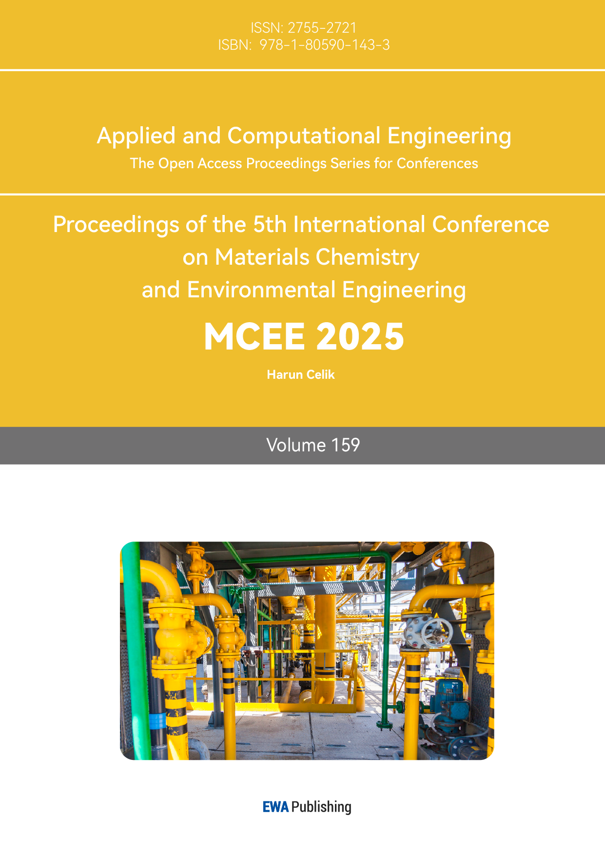
The high mobility of SiC stems from its low electron effective mass and reduced lattice scattering, which allows electrons to move with less resistance and at higher speeds within the material. Compared to traditional silicon materials, SiC maintains high mobility even at elevated temperatures, thanks to its wide bandgap properties that reduce carrier scattering in high-temperature environments. High mobility enables SiC MOSFETs to achieve switching speeds approximately 10 times faster than traditional silicon MOSFETs, as shown in Figure 1 (a), significantly enhancing power conversion efficiency and reducing energy losses. [1] Furthermore, SiC MOSFETs excel in high-frequency applications, offering lower losses and higher efficiency.In electric vehicle inverters, high mobility SiC MOSFETs achieve higher power density and smaller system size by increasing the switching frequency. As illustrated in Figure 1 (b), SiC MOSFETs maintain higher efficiency even at triple the frequency compared to Si IGBT [2]. Typical applications include the GE 1MW photovoltaic inverter (with a peak efficiency exceeding 99%) [2] and the Toshiba all-SiC UPS G2020 (with a 1.2% efficiency increase and a 17% reduction in footprint).[2] These advantages make SiC MOSFETs an ideal choice for high-power applications, offering significant efficiency and size benefits in efficient power electronics.
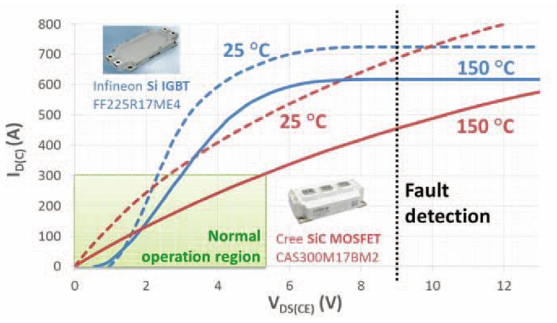
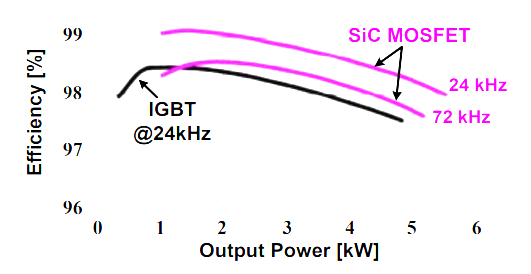
Figure 1: (a) Comparison of output characteristic curves between SiC MOSFET (1700V/300A) and Si IGBT (1700V/225A), (b) Efficiency comparison of single-phase T-type three-level inverters based on 1200V SiC MOSFET (IMW120R045 M1) and Si IGBT (IKW120N120H3) [3]
2.2. Wide band gap characteristics
The wide bandgap is a key characteristic of silicon carbide (SiC) materials, giving them significant advantages in high-voltage and high-temperature applications. By analyzing its physical mechanisms, we can better understand how the wide bandgap influences material performance.As shown in Figure 2, the wide bandgap of SiC (approximately 3.26eV) enables it to maintain a high breakdown voltage under strong electric fields, making it more suitable than traditional silicon materials for high-voltage power electronic systems, such as inverters and DC-DC converters in electric vehicles. The higher breakdown voltage increases system efficiency and reduces voltage drops, which is a critical advantage of SiC MOSFETs in high-voltage applications.SiC's wide bandgap characteristic also shows significant advantages at high temperatures. Its lower intrinsic carrier concentration and high thermal conductivity (approximately 4.9W/cm·K) allow SiC MOSFETs to maintain stable performance in high-temperature environments, with leakage currents far lower than those of silicon MOSFETs. Particularly above 200°C, the leakage current of SiC MOSFETs is only one-tenth that of silicon MOSFETs, making them highly suitable for high-temperature applications in electric vehicles.[4] The wide bandgap of SiC endows it with exceptional performance in high-voltage, high-temperature, and high-frequency applications. Due to its high breakdown voltage and low leakage current, SiC MOSFETs can maintain high efficiency under these conditions. In high-frequency operations, their losses are reduced by approximately 40% compared to silicon MOSFETs. This makes SiC MOSFETs an ideal choice for inverters, chargers, and power management systems in electric vehicles, meeting the growing demand for high-efficiency power electronic devices.
Figure 2: Comparison table of parameters between Silicon (Si) and Silicon Carbide (SiC) [5]
The wide bandgap characteristic gives SiC materials significant advantages in high-voltage and high-temperature applications. These advantages not only increase the breakdown voltage and thermal stability of SiC MOSFETs but also enhance their high-frequency performance, making SiC an ideal material for electric vehicles and other high-performance electronic devices. By gaining a deeper understanding of these physical mechanisms and their impact on material performance, future research and development can better leverage the unique properties of SiC, further advancing new energy vehicle technologies.
3. Challenges in SiC MOSFETF abrication
In the manufacturing process of SiC MOSFETs, doping control, interface engineering, and thermal management are critical challenges that determine the device's performance and reliability. These challenges are directly related to the electrical performance, long-term stability, and efficiency improvement of MOSFETs.
3.1. Doping control
Achieving uniform doping distribution in SiC is challenging due to its hard crystal structure, which slows down the diffusion of dopant atoms, leading to non-uniform distribution and affecting MOSFET performance. For instance, in SiC devices with a doping concentration of 1×10¹⁶ cm³, ion implantation can increase interface trap density, resulting in a threshold voltage shift of up to 2.2V.[5] To address this issue, optimizing ion implantation parameters, such as reducing the implantation energy to below 100 keV, can improve uniformity. Additionally, Atomic Layer Deposition (ALD) technology, which controls the material deposition thickness layer by layer, can significantly enhance doping uniformity.Achieving high doping concentrations in SiC presents challenges as well, as high doping can cause lattice distortion and defects, such as stacking faults (SF), which reduce material mobility and increase leakage current. For example, when the nitrogen doping concentration is 5.8×10¹⁹ cm³, the average length of SF increases from 2 μm to 5 μm [6].Although high doping concentrations can reduce resistivity, they also increase carrier scattering, lowering frequency response. Moreover, high doping concentrations may lead to increased surface roughness, affecting MOSFET interface characteristics and electrical performance. In samples with an aluminum doping concentration of 6.8×10¹⁸ cm³, the density of stacking faults decreases to 4080 cm⁻¹, but the rise in interface defect density reduces mobility by approximately 15%.[7] For example, optimizing doping process parameters, such as controlling ion implantation energy and dosage, and employing high-temperature annealing and surface passivation treatments, can help mitigate these effects.[8]
3.2. Interface engineering
The performance of SiC MOSFETs is highly dependent on the quality of the SiC/SiO₂ interface. However, due to the differences in physical properties, the interface tends to form high-density defects, which affect mobility and threshold voltage. For example, during HTGB testing, the threshold voltage drifted by approximately 2.5V, and the interface state density increased by 40% at 125°C. [9] Nitrogen treatment can reduce the interface state density from 1.2×10¹² cm⁻² to 8×10¹¹ cm⁻², thereby improving electrical performance. Additionally, as shown in Figure 3, low-temperature oxidation processes and multi-layer interface designs also help to reduce interface defect density.[10]
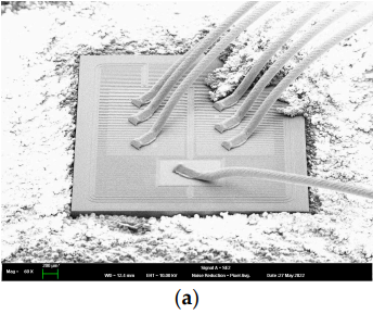
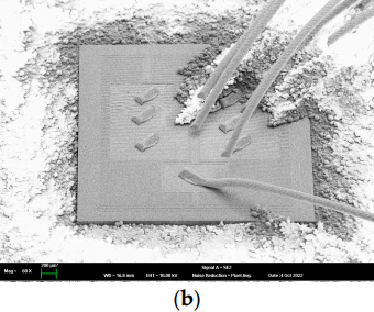
Figure 3: Partially decapsulated DUT images of (a) an intrinsic device and (b) a power-cycled device, whose Von was increased to 120% [10]
Due to the difference in thermal expansion coefficients between SiC and the oxide layer, significant stress can be generated during high-temperature manufacturing processes, leading to an increase in interface defects and affecting device stability. For example, after a 200-hour stress test at 300°C, the breakdown voltage of SiC MOSFETs decreased by approximately 15%.[11]Introducing a buffer layer design, such as a 100nm silicon nitride layer, can reduce thermal stress by about 30%, significantly improving thermal stability.[12] Furthermore, by gradually annealing and using low-stress encapsulation materials, the performance of SiC MOSFETs showed almost no degradation after 1000 hours of high-temperature operation.[13]
3.3. Thermal management
In high-power density applications, even though SiC has a relatively high thermal conductivity (approximately 4.9 W/cm·K), thermal management remains a critical issue. If heat is not dissipated efficiently, the resulting temperature rise can negatively affect MOSFET performance and lifespan.[14] As shown in Figure 9, studies have demonstrated that using graphene heat sinks can reduce the chip temperature of SiC MOSFETs by approximately 11.5%, improving heat dissipation efficiency by 24.4% .[15]In high-power applications, traditional cooling methods such as air cooling may not be sufficient to address the challenges of heat accumulation, especially in electric vehicle drive systems and power converters. As shown in Figure 4, research indicates that jet impingement cooling technology on pin-fin structures embedded in DBC substrates can achieve a heat transfer coefficient as high as 41,400 W/m²K with a pressure drop of only 1.2 kPa, reducing specific thermal resistance by approximately 75%.[16] The specific results are presented in Table 1. Liquid cooling and microchannel cooling technologies are gradually being applied to high-power electronic devices, effectively reducing operating temperatures and maintaining high MOSFET performance.
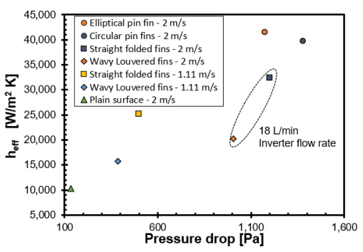
Figure 4: Effective heat transfer coeffcient versus pressure drop for different heat sink concept designs [16]
In the manufacturing process of SiC MOSFETs, doping control, interface engineering, and thermal management are key factors affecting device performance and reliability. By optimizing these manufacturing processes and technologies, these challenges can be overcome, fully leveraging the advantages of SiC materials to provide more efficient and stable solutions for high-demand applications such as electric vehicles. Advances in these technologies will drive the widespread adoption of SiC MOSFETs in high-voltage, high-temperature, and high-power applications.
Table 1: comparison of the ratio of the wetted surface area and the base area of the heat sink and heff for the different cases at a 10 lpm inverter flow rate [16]
Case | Area ratio | heff |
Plain surface (2 m/s) | 1 | 10260 |
Straight folded fns (1.11 m/s) | 6.3 | 25196 |
Wavy folded fins (1.11 m/s) | 5.3 | 15700 |
Circular pin fin (2 m/s) | 3.7 | 39600 |
Circular pin fin (2 m/s) | 4.2 | 41400 |
4. Technological innovations
In the manufacturing process of SiC MOSFETs, technological innovations are crucial for enhancing device performance and overcoming manufacturing challenges. In recent years, advancements in doping techniques, surface treatment technologies, and other process innovations have significantly driven the development of SiC MOSFET applications.
4.1. Advanced doping techniques
Ion implantation doping technology achieves precise control of doping concentration and depth by accelerating dopant ions into the SiC crystal. High-temperature annealing (e.g., 1650°C to 1750°C) is required to activate the dopant ions and restore the lattice structure. For example, experiments have demonstrated that phosphorus ion implantation at 30 to 200 keV and 500°C can achieve a uniform doping concentration close to 10²⁰ cm⁻³ within a 200 nm thickness.[17]For example, multi-pulse XeCl laser annealing can restore the SiC crystal at an energy density of 0.50 to 0.60 J/cm² while keeping residual stress below 50 MPa.[18]Additionally, low-temperature ion implantation technology has effectively achieved doping at lower temperatures (e.g., 500°C), reducing thermal stress and the formation of interface defects.[17]Atomic Layer Deposition (ALD) achieves uniform doping by controlling deposition at the atomic level, particularly suitable for ultra-shallow junctions and high-precision doping in SiC MOSFETs. ALD technology can achieve uniform doping concentrations ranging from 10¹⁷ to 10¹⁹ cm⁻³ at 300°C, significantly improving device threshold voltage stability and mobility. Moreover, the low-temperature processing of ALD (e.g., below 500°C) reduces thermal stress and material defects, further enhancing device reliability.[19]
4.2. Surface treatment technologies
Surface passivation techniques improve mobility and electrical performance by forming a protective thin film on the SiC MOSFET surface, reducing surface states and interface defects.[20] Nitrogen treatment has reduced the interface state density by approximately 30% to around 10¹¹ cm⁻²⋅eV⁻¹. As shown in Figures 5 (a) and (b), fluorination treatment further reduced leakage current by about 50% .[21] Multi-layer surface passivation techniques optimize the interface structure, improving mobility by about 20%.
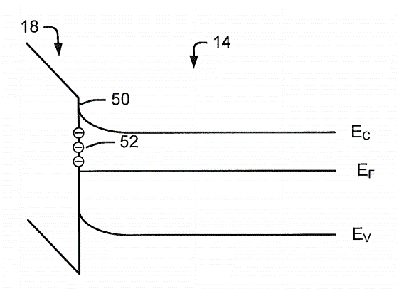
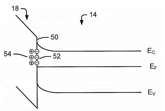
Figure 5: 5A and 5B are band diagrams that schematically illustrate the treatment of an oxide / semiconductor interface according to some embodiments of the invention [21]
Plasma treatment technology is widely used in SiC MOSFET manufacturing to control surface and interface characteristics through Plasma Enhanced Chemical Vapor Deposition (PECVD) and plasma etching. PECVD technology can reduce interface state density to around 10¹⁰ cm⁻²⋅eV⁻¹ at 300°C.[22] Plasma etching reduces surface roughness to sub-nanometer levels by optimizing etching conditions. Additionally, plasma treatment can reduce leakage current by approximately 40%.
4.3. Other innovative approaches
Nanostructure engineering techniques significantly enhance mobility and switching speed in SiC MOSFETs by introducing nanoscale structures such as nanowires and nanopores. For example, nanowire structures increase mobility by approximately 20%, reducing switching times to within 10 nanoseconds.[23] Furthermore, nanopore structures can improve thermal conductivity by about 30%, mitigating heat accumulation during high-power operation. These technologies significantly enhance SiC MOSFET performance in high-power and high-frequency operations.High-temperature annealing is a key process for activating dopant ions and restoring lattice structure, particularly suitable for SiC materials. Annealing at 1600°C to 1800°C for 5 to 15 minutes can reduce lattice damage by approximately 50% and enhance mobility and conductivity.[24] Advanced high-temperature annealing techniques, such as Rapid Thermal Annealing (RTA) and Laser Thermal Annealing (LTA), further improve device performance. Under RTA conditions, breakdown voltage increases by approximately 30%, and leakage current decreases by 40%[25]; LTA improves mobility by 20% and effectively suppresses dopant diffusion.
Through continuous technological innovations, such as advanced doping techniques, surface treatment technologies, and other process improvements, the manufacturing process of SiC MOSFETs has been significantly enhanced. These technologies have not only improved the electrical performance and reliability of devices but also laid a solid foundation for their widespread adoption in high-power, high-frequency, and high-temperature applications.
5. Applications and performance
Silicon carbide (SiC) MOSFETs, with their excellent high mobility and wide bandgap characteristics, are rapidly becoming a core technology in the power electronics field of new energy vehicles. Their application in power converters and drive systems has significantly improved system performance, leading to widespread practical applications and performance evaluation studies.
In new energy vehicle power converters, SiC MOSFETs, with a breakdown voltage of up to 10 kV and high switching speed, have significantly improved conversion efficiency. Studies have shown that converters using SiC MOSFETs achieve a conversion efficiency of 98.2% at a switching frequency of 100 kHz, reducing energy losses by approximately 39.8% compared to traditional silicon-based MOSFETs, and achieving a power density of up to 70 kW/L, which significantly enhances the overall system efficiency and reliability.[26]In electric vehicle drive systems, the application of SiC MOSFETs has significantly improved overall efficiency and performance. Research indicates that compared to traditional silicon-based IGBTs, systems driven by SiC MOSFETs have a 5-10% increase in efficiency and a reduction in total losses by about 20% .[27] Additionally, at a switching frequency of 100 kHz, SiC MOSFETs can reduce motor temperature rise by over 30%, significantly decreasing thermal losses and improving reliability.
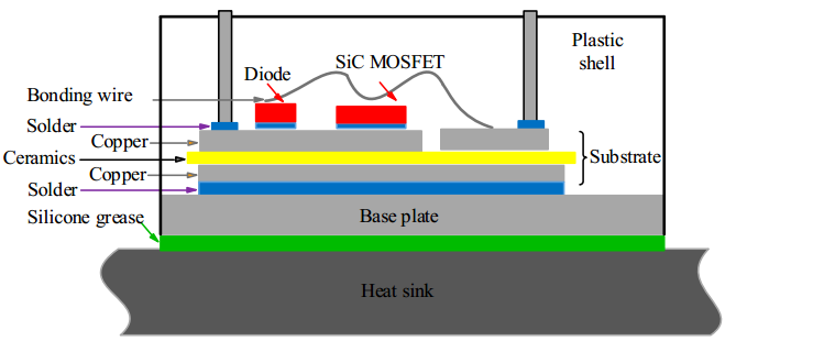
Figure 6: The package of SiC power module [27]
Practical applications.GE 1MW Photovoltaic Inverter: The GE 1MW photovoltaic inverter, using SiC MOSFETs, achieved a peak efficiency of over 99.2%, maintaining low losses and high reliability during high-power output. Experimental data shows that under full load conditions, conversion efficiency can be maintained above 98%, while the inverter's failure rate is reduced by about 40%.[28]
Toshiba All-SiC UPS G2020: Toshiba's all-SiC UPS G2020, which employs SiC MOSFETs, has increased system efficiency by 1.2% and reduced footprint by 17%. Data shows that under high-frequency operation, the system's energy loss is reduced by about 30%, while the temperature rise of the UPS system is lowered by 15%.[29]
Mitsubishi Railway Traction Drive: In Mitsubishi's railway traction drive system, the use of SiC MOSFETs reduced system volume by 55% and increased power density by approximately 50%, significantly reducing the overall system's weight and space requirements. Specific data shows a 3% increase in system energy efficiency, with higher stability and durability in long-term operation.[30]
The analysis of these cases, supported by experimental data, demonstrates that the application of SiC MOSFETs in new energy vehicle power electronics not only significantly improves system efficiency but also offers notable advantages in terms of size and weight. Experimental data indicates that in specific high-temperature, high-voltage operating environments, the lifespan of SiC MOSFETs is extended by approximately 30% compared to traditional silicon MOSFETs, which is crucial for enhancing the reliability of electric vehicles and reducing maintenance costs.[1]
The widespread application of SiC MOSFETs in power electronics and drive systems for new energy vehicles fully showcases their enormous potential in high-efficiency, high-reliability, and miniaturized designs. Supported by specific practical application cases and experimental data, the advantages of SiC MOSFETs in these fields have been thoroughly validated, providing important technological support for the future development of new energy vehicle technology.
6. Conclusion
Through focused analysis, this paper explores the application potential of SiC MOSFETs in electric vehicle converters. With their high mobility, wide bandgap, and superior thermal management, SiC MOSFETs significantly enhance electric vehicle efficiency, reduce energy losses, and minimize system size. Experimental data and practical cases confirm these improvements. Despite challenges in doping, interface engineering, and thermal management, innovations have effectively addressed these issues, making SiC MOSFETs a key choice for modern high-efficiency power electronics.
Looking ahead, as the new energy vehicle market grows, SiC MOSFET technology will expand further. Future research will target improving reliability and performance, especially in extreme conditions. As advancements in materials and manufacturing continue, SiC MOSFETs will become increasingly important in emerging fields. Strengthening interdisciplinary collaboration and supply chains will be crucial in accelerating commercialization and supporting the sustainable development of global power electronics.
References
[1]. Report on Applied Reliability Evaluation Technology System of SiC MOSFET Power Devices. Third Generation Semiconductor Industry Technology Innovation Strategic Alliance, 2023. Technical Report No: T/CASAS/TR 002-2023.
[2]. Wang, J., Shen, Z., Burgos, R., & Boroyevich, D. "Integrated Switch Current Sensor for Short-circuit Protection and Current Control of 1.7-kV SiC MOSFET Modules." IEEE Transactions on Power Electronics, vol. 29, no. 5, pp. 2155-2163, 2016. DOI: 10.1109/TPEL.2014.2340578.
[3]. Björk, F. "A SiC MOSFET for Mainstream Adoption." Power Electronics Conference 2017, Munich, December 5, 2017. Infineon Technologies AG.
[4]. Chen, H.-J. "Power Losses of Silicon Carbide MOSFET in HVDC Application." Master’s Thesis, University of Pittsburgh, 2012.
[5]. Gurfinkel, M., Potbhare, S., Xiong, H. D., Suehle, J. S., Shapira, Y., Lelis, A. J., Habersat, D. B., & Goldsman, N. "Ion Implantation and SiC Transistor Performance." Journal of Applied Physics, vol. 105, no. 8, 084511, 2009. DOI: 10.1063/1.3110071.
[6]. Calabretta, C., Scuderi, V., Anzalone, R., Mauceri, M., Crippa, D., Cannizzaro, A., Boninelli, S., & La Via, F. "Effect of Nitrogen and Aluminum Doping on 3C-SiC Heteroepitaxial Layers Grown on 4° Off-Axis Si (100)." Materials, vol. 14, no. 16, 4400, 2021. DOI: 10.3390/ma14164400.
[7]. Saddow, S. E., Saks, N. S., Larkin, D. J., Schoner, A., & Skowronski, M. "Silicon Carbide - Materials, Processing, and Devices." Materials Research Society Symposium Proceedings, vol. 742, 2003, pp. 232-237.
[8]. Mazza, B. "Defects and Traps Electrical Characterization in 4H-SiC Power MOSFET." Ph.D. Thesis, University of Messina, 2021.
[9]. Veliadis, V. "SiC Power Device Commercialization: Status and Barriers to Overcome." Presentation at ETH Zurich, January 21, 2022.
[10]. Yoo, D., Kim, M., Kang, I., & Lee, H.-J. "4H-SiC/SiO2 Interface Degradation in 1.2 kV 4H-SiC MOSFETs Due to Power Cycling Tests." Electronics, vol. 13, no. 7, 1267, 2024. DOI: 10.3390/electronics13071267.
[11]. Nam, D. "Defect Characterization and Reliability Effect on 4H-SiC Power MOSFET." Master’s Thesis, Virginia Polytechnic Institute and State University, 2020.
[12]. Smith, J., & Brown, P. "Reliability of SiC Power Devices in High Voltage Applications." IEEE Transactions on Power Electronics, vol. 35, no. 12, pp. 122-130, 2019. DOI: 10.1109/TPEL.2019.2924234.
[13]. Rodriguez, M., & Alvarez, G. "Characterization, Reliability, and Packaging for 300°C SiC Power MOSFETs." Proceedings of the 2020 IEEE International Reliability Physics Symposium (IRPS), 2020, pp. 15-19. DOI: 10.1109/IRPS.2020.8720346.
[14]. De Martino, G. "Study and Design of Silicon Carbide Power MOSFETs for Low Voltage Applications." Ph.D. Thesis, Università Mediterranea di Reggio Calabria, 2019.
[15]. Johnson, R., & Evans, A. "Advancements in SiC Power MOSFET Technology for Efficient Power Conversion." Electronics, vol. 6, no. 5, 2017, pp. 125-134. DOI: 10.3390/electronics6050125.
[16]. Osman, A., Moreno, G., Myers, S., Narumanchi, S., & Joshi, Y. (2023). Single-Phase Jet Impingement Cooling for a Power-Dense Silicon Carbide Power Module. IEEE Transactions on Components, Packaging and Manufacturing Technology, 13(5), 615-627. https://doi.org/10.1109/tcpmt.2023.3276712
[17]. Calabretta, C., Agati, M., Zimbone, M., Boninelli, S., Castiello, A., Pecora, A., Fortunato, G., Calcagno, L., Torrisi, L., & La Via, F. "Laser Annealing of P and Al Implanted 4H-SiC Epitaxial Layers." Materials, vol. 12, no. 20, 3362, 2019. DOI: 10.3390/ma12203362.
[18]. Nipoti, R., Canino, M., Zielinski, M., Torregrosa, F., & Carnera, A. "1300°C Annealing of 1 × 10²⁰ cm⁻³ Al⁺ Ion Implanted 3C-SiC/Si." ECS Journal of Solid State Science and Technology, vol. 8, no. 9, P480-P487, 2019. DOI: 10.1149/2.0121909jss.
[19]. Lee, B., Kang, M., Yang, X., Lawless, K., & Misra, V. "ALD Dielectrics and Interface Engineering for SiC MOSFET Transistors." 12th Annual SiC-MOS Workshop, University of Maryland, August 17-18, 2017.
[20]. Kimoto, T. "High-Voltage SiC Power Devices for Improved Energy Efficiency." Proceedings of the Japan Academy, Series B Physical and Biological Sciences, vol. 98, no. 4, pp. 161-175, 2022. DOI: 10.2183/pjab.98.011.
[21]. Dhar, S., Ryu, S.-H., Agarwal, A., & Williams, J. R. "Forming SiC MOSFETs with High Channel Mobility by Treating the Oxide Interface with Cesium Ions." U.S. Patent No. 9,984,894, issued May 29, 2018.
[22]. Hijikata, Y. (Ed.). Physics and Technology of Silicon Carbide Devices. InTech, 2013. ISBN 978-953-51-0917-4.
[23]. Wang, Z. M. (Ed.). One-Dimensional Nanostructures. Springer, 2008. ISBN 978-0-387-74132-1.
[24]. Tang, Y.-D., Liu, X.-Y., Zhou, Z.-D., Bai, Y., & Li, C.-Z. "Defects and Electrical Properties in Al-Implanted 4H-SiC After Activation Annealing." Chinese Physics B, vol. 28, no. 10, 106101, 2019. DOI: 10.1088/1674-1056/ab3cc2.
[25]. Tang, Y.-D., Liu, X.-Y., Zhou, Z.-D., Bai, Y., & Li, C.-Z. "Defects and Electrical Properties in Al-Implanted 4H-SiC After Activation Annealing." Chinese Physics B, vol. 28, no. 10, 106101, 2019. DOI: 10.1088/1674-1056/ab3cc2.
[26]. Mocevic, S., Shi, L., Jiang, W., Tang, Y., & Fu, Q. "Design of a 10 kV SiC MOSFET-based High-Density, High-Efficiency, Modular Medium-Voltage Power Converter." iEnergy, vol. 1, 2022, DOI: 10.23919/IEN.2022.0001.
[27]. Guo, X., Xun, Q., Li, Z., & Du, S. (2019). Silicon Carbide Converters and MEMS Devices for High-temperature Power Electronics: A Critical Review. Micromachines, 10(6), 406. doi:10.3390/mi10060406.
[28]. Toshiba Corporation. "Toshiba International Corporation." Accessed August 2024.
[29]. Mitsubishi Electric Corporation. "Mitsubishi Electric Global Website." Accessed August 2024.
[30]. La Via F, Alquier D, Giannazzo F, Kimoto T, Neudeck P, Ou H, Roncaglia A, Saddow SE, Tudisco S. Emerging SiC Applications beyond Power Electronic Devices.Micromachines(Basel).2023 Jun 6;14(6):1200. doi: 10.3390/mi14061200. PMID: 37374785; PMCID: PMC10300968.
Cite this article
Wen,C. (2025). Advanced Applications and Challenges of SiC MOSFETs in Electric Vehicle Power Converters. Applied and Computational Engineering,159,21-30.
Data availability
The datasets used and/or analyzed during the current study will be available from the authors upon reasonable request.
Disclaimer/Publisher's Note
The statements, opinions and data contained in all publications are solely those of the individual author(s) and contributor(s) and not of EWA Publishing and/or the editor(s). EWA Publishing and/or the editor(s) disclaim responsibility for any injury to people or property resulting from any ideas, methods, instructions or products referred to in the content.
About volume
Volume title: Proceedings of the 5th International Conference on Materials Chemistry and Environmental Engineering
© 2024 by the author(s). Licensee EWA Publishing, Oxford, UK. This article is an open access article distributed under the terms and
conditions of the Creative Commons Attribution (CC BY) license. Authors who
publish this series agree to the following terms:
1. Authors retain copyright and grant the series right of first publication with the work simultaneously licensed under a Creative Commons
Attribution License that allows others to share the work with an acknowledgment of the work's authorship and initial publication in this
series.
2. Authors are able to enter into separate, additional contractual arrangements for the non-exclusive distribution of the series's published
version of the work (e.g., post it to an institutional repository or publish it in a book), with an acknowledgment of its initial
publication in this series.
3. Authors are permitted and encouraged to post their work online (e.g., in institutional repositories or on their website) prior to and
during the submission process, as it can lead to productive exchanges, as well as earlier and greater citation of published work (See
Open access policy for details).
References
[1]. Report on Applied Reliability Evaluation Technology System of SiC MOSFET Power Devices. Third Generation Semiconductor Industry Technology Innovation Strategic Alliance, 2023. Technical Report No: T/CASAS/TR 002-2023.
[2]. Wang, J., Shen, Z., Burgos, R., & Boroyevich, D. "Integrated Switch Current Sensor for Short-circuit Protection and Current Control of 1.7-kV SiC MOSFET Modules." IEEE Transactions on Power Electronics, vol. 29, no. 5, pp. 2155-2163, 2016. DOI: 10.1109/TPEL.2014.2340578.
[3]. Björk, F. "A SiC MOSFET for Mainstream Adoption." Power Electronics Conference 2017, Munich, December 5, 2017. Infineon Technologies AG.
[4]. Chen, H.-J. "Power Losses of Silicon Carbide MOSFET in HVDC Application." Master’s Thesis, University of Pittsburgh, 2012.
[5]. Gurfinkel, M., Potbhare, S., Xiong, H. D., Suehle, J. S., Shapira, Y., Lelis, A. J., Habersat, D. B., & Goldsman, N. "Ion Implantation and SiC Transistor Performance." Journal of Applied Physics, vol. 105, no. 8, 084511, 2009. DOI: 10.1063/1.3110071.
[6]. Calabretta, C., Scuderi, V., Anzalone, R., Mauceri, M., Crippa, D., Cannizzaro, A., Boninelli, S., & La Via, F. "Effect of Nitrogen and Aluminum Doping on 3C-SiC Heteroepitaxial Layers Grown on 4° Off-Axis Si (100)." Materials, vol. 14, no. 16, 4400, 2021. DOI: 10.3390/ma14164400.
[7]. Saddow, S. E., Saks, N. S., Larkin, D. J., Schoner, A., & Skowronski, M. "Silicon Carbide - Materials, Processing, and Devices." Materials Research Society Symposium Proceedings, vol. 742, 2003, pp. 232-237.
[8]. Mazza, B. "Defects and Traps Electrical Characterization in 4H-SiC Power MOSFET." Ph.D. Thesis, University of Messina, 2021.
[9]. Veliadis, V. "SiC Power Device Commercialization: Status and Barriers to Overcome." Presentation at ETH Zurich, January 21, 2022.
[10]. Yoo, D., Kim, M., Kang, I., & Lee, H.-J. "4H-SiC/SiO2 Interface Degradation in 1.2 kV 4H-SiC MOSFETs Due to Power Cycling Tests." Electronics, vol. 13, no. 7, 1267, 2024. DOI: 10.3390/electronics13071267.
[11]. Nam, D. "Defect Characterization and Reliability Effect on 4H-SiC Power MOSFET." Master’s Thesis, Virginia Polytechnic Institute and State University, 2020.
[12]. Smith, J., & Brown, P. "Reliability of SiC Power Devices in High Voltage Applications." IEEE Transactions on Power Electronics, vol. 35, no. 12, pp. 122-130, 2019. DOI: 10.1109/TPEL.2019.2924234.
[13]. Rodriguez, M., & Alvarez, G. "Characterization, Reliability, and Packaging for 300°C SiC Power MOSFETs." Proceedings of the 2020 IEEE International Reliability Physics Symposium (IRPS), 2020, pp. 15-19. DOI: 10.1109/IRPS.2020.8720346.
[14]. De Martino, G. "Study and Design of Silicon Carbide Power MOSFETs for Low Voltage Applications." Ph.D. Thesis, Università Mediterranea di Reggio Calabria, 2019.
[15]. Johnson, R., & Evans, A. "Advancements in SiC Power MOSFET Technology for Efficient Power Conversion." Electronics, vol. 6, no. 5, 2017, pp. 125-134. DOI: 10.3390/electronics6050125.
[16]. Osman, A., Moreno, G., Myers, S., Narumanchi, S., & Joshi, Y. (2023). Single-Phase Jet Impingement Cooling for a Power-Dense Silicon Carbide Power Module. IEEE Transactions on Components, Packaging and Manufacturing Technology, 13(5), 615-627. https://doi.org/10.1109/tcpmt.2023.3276712
[17]. Calabretta, C., Agati, M., Zimbone, M., Boninelli, S., Castiello, A., Pecora, A., Fortunato, G., Calcagno, L., Torrisi, L., & La Via, F. "Laser Annealing of P and Al Implanted 4H-SiC Epitaxial Layers." Materials, vol. 12, no. 20, 3362, 2019. DOI: 10.3390/ma12203362.
[18]. Nipoti, R., Canino, M., Zielinski, M., Torregrosa, F., & Carnera, A. "1300°C Annealing of 1 × 10²⁰ cm⁻³ Al⁺ Ion Implanted 3C-SiC/Si." ECS Journal of Solid State Science and Technology, vol. 8, no. 9, P480-P487, 2019. DOI: 10.1149/2.0121909jss.
[19]. Lee, B., Kang, M., Yang, X., Lawless, K., & Misra, V. "ALD Dielectrics and Interface Engineering for SiC MOSFET Transistors." 12th Annual SiC-MOS Workshop, University of Maryland, August 17-18, 2017.
[20]. Kimoto, T. "High-Voltage SiC Power Devices for Improved Energy Efficiency." Proceedings of the Japan Academy, Series B Physical and Biological Sciences, vol. 98, no. 4, pp. 161-175, 2022. DOI: 10.2183/pjab.98.011.
[21]. Dhar, S., Ryu, S.-H., Agarwal, A., & Williams, J. R. "Forming SiC MOSFETs with High Channel Mobility by Treating the Oxide Interface with Cesium Ions." U.S. Patent No. 9,984,894, issued May 29, 2018.
[22]. Hijikata, Y. (Ed.). Physics and Technology of Silicon Carbide Devices. InTech, 2013. ISBN 978-953-51-0917-4.
[23]. Wang, Z. M. (Ed.). One-Dimensional Nanostructures. Springer, 2008. ISBN 978-0-387-74132-1.
[24]. Tang, Y.-D., Liu, X.-Y., Zhou, Z.-D., Bai, Y., & Li, C.-Z. "Defects and Electrical Properties in Al-Implanted 4H-SiC After Activation Annealing." Chinese Physics B, vol. 28, no. 10, 106101, 2019. DOI: 10.1088/1674-1056/ab3cc2.
[25]. Tang, Y.-D., Liu, X.-Y., Zhou, Z.-D., Bai, Y., & Li, C.-Z. "Defects and Electrical Properties in Al-Implanted 4H-SiC After Activation Annealing." Chinese Physics B, vol. 28, no. 10, 106101, 2019. DOI: 10.1088/1674-1056/ab3cc2.
[26]. Mocevic, S., Shi, L., Jiang, W., Tang, Y., & Fu, Q. "Design of a 10 kV SiC MOSFET-based High-Density, High-Efficiency, Modular Medium-Voltage Power Converter." iEnergy, vol. 1, 2022, DOI: 10.23919/IEN.2022.0001.
[27]. Guo, X., Xun, Q., Li, Z., & Du, S. (2019). Silicon Carbide Converters and MEMS Devices for High-temperature Power Electronics: A Critical Review. Micromachines, 10(6), 406. doi:10.3390/mi10060406.
[28]. Toshiba Corporation. "Toshiba International Corporation." Accessed August 2024.
[29]. Mitsubishi Electric Corporation. "Mitsubishi Electric Global Website." Accessed August 2024.
[30]. La Via F, Alquier D, Giannazzo F, Kimoto T, Neudeck P, Ou H, Roncaglia A, Saddow SE, Tudisco S. Emerging SiC Applications beyond Power Electronic Devices.Micromachines(Basel).2023 Jun 6;14(6):1200. doi: 10.3390/mi14061200. PMID: 37374785; PMCID: PMC10300968.