


1. Introduction
The development of solar photovoltaic cells has provided mankind with a new source of energy to utilize. Photovoltaics are also being iterated in order to use solar energy more efficiently. After the introduction of the first generation of photovoltaic power generation (crystalline silicon photovoltaic power generation) and the second generation of photovoltaic power generation (thin film cells) technology, the third generation of photovoltaic power generation technology was born. Among the wide range of third-generation photovoltaic power generation technologies, there is a widely used type of photovoltaic-heterojunction photovoltaic cells. Although each of the different types of heterojunction photovoltaics has been studied in depth, no one has considered the direct application of the different types of heterojunction photovoltaics at the application level.
Thus, this paper will compare various aspects of heterojunction photovoltaic cells made of different materials—including but not limited to photovoltaic performance, manufacturing process, possible cost, etc. An introductory analysis of certain heterojunction PV cells will be presented through the comparison of the above dimensions. In this paper, three different types of heterojunction photovoltaic cells will be introduced. Their structure, fabrication process, performance, and other related information will be introduced. Then we will discuss which of these heterojunction PV cells is better by way of a side-by-side comparison.
Through this research, several of the more prominent heterogeneous junctions of PV can be judged to be superior or inferior. This will provide a little consideration of commercial options for subsequent heterojunction PV applications. This consideration helps to determine how heterojunction PV should be applied in real-world scenarios and provides a reference for determining what kind of heterojunction PV should be developed in the future. Similarly, this simple comparison can be applied to more types of heterojunction photovoltaics, and indeed to all third generation photovoltaics, and then allows for a wider range of performance evaluation of different PVs.
2. Heterojunction photovoltaics and its benefits
The structure of the heterojunction solar cell is shown in Figure 1 and is relatively symmetrical. The manufacturing process is as follows: an intrinsic amorphous silicon film (a-Si(i)) is deposited on each side of the n-type monocrystalline silicon wafer (c-Si(n)), and then p-type and n-type amorphous silicon films are deposited on the outside of it. (a-Si(i)) on each side of the n-type monocrystalline silicon wafer (c-Si(n)), and then depositing p-type and n-type amorphous Then, transparent conductive oxidation (TCO) is deposited on the two surfaces, and metal gate electrodes are coated. When compared to conventional polycrystalline solar cells, heterojunction solar cells have a higher photovoltaic efficiency. Heterojunction solar cells have higher photoelectric conversion efficiency, can generate electricity on both sides, and have a smaller power temperature coefficient [1].
style='position:absolute;left:0pt;margin-left:250.85pt;margin-top:3.4pt;height:25.8pt;width:112.75pt;z-index:251659264;mso-width-relative:page;mso-height-relative:page;' />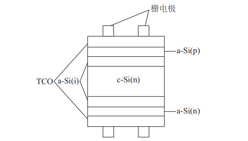
Figure 1. Structure diagram of heterojunction solar cell [1]
When sunlight irradiates onto the positive surface of the cell, the absorption process occurs in the absorber layer of the cell, forming photogenerated carriers. Photogenerated carriers diffuse to the p-n junction area on the positive surface and the high-low junction area on the back surface of n (p) type HIT solar cells, and due to the traction of the built-in electric field, holes (electrons) and electrons (holes) are each deflected to the emitter and back electric field, and charges gradually accumulate on the positive and back surfaces of the solar cell. The photovoltaic effect is formed.
One benefit of heterojunction solar cells is that those cells employ lower temperature (below 250℃) conditions relative to the thin-film solar cell process. This new process reduces energy consumption and does not consume conventional energy, while amorphous silicon-hydrogen thin film doping, film layers, and forbidden bands are effectively regulated at low temperatures, which is beneficial in the production of HIT solar cells processes to enhance device functionality; this in the low-temperature deposition of thin films process can reduce the Si-sub in the high-temperature processing of functional degradation, thus allowing in the heterojunction solar manufacturing process to use "low quality" crystalline silicon or even use Poly-Si as a substrate.
In addition, heterojunction solar cells have good stability under solar irradiation, and multiple studies have shown that heterojunction solar cells do not experience the phenomenon of light decay, so there is no problem like c-Si and a-Si solar cells where the output power is reduced due to photodegradation. The temperature stability of heterojunction cells is excellent. Compared with the temperature coefficient of -0.5%/℃ of CZ-Si cells, the temperature coefficient of heterojunction cells can be reduced to -0.25%/℃, which allows the cells to maintain efficient output when the temperature rises under light.
In addition, the Staebler-Wronski effect [2], which is common in amorphous silicon solar cells, does not occur in HJT solar cells. Besides, HJT cells use N-type silicon wafers with phosphorus as the dopant, and there is almost no photogenic attenuation.
3. Graphene/inorganic heterojunction solar cells
Graphene has excellent optoelectronic properties such as high light transmission and high electrical conductivity, as well as good mechanical flexibility. In 2009, Professor Ruoff's research team at the University of Texas at Austin successfully prepared large-area monolayers of graphene on metallic copper foil substrates by chemical vapor deposition (CVD) for the first time[3]. After this, Prof. Byung Hee Hong's group at Sungkyunkwan University in Korea and Sony Corporation in Japan, respectively, in 2010, and 2013, graphene transparent conductive films with sizes of up to 30 inches and up to 100 meters were prepared and applied to the touch screens of electronic devices[4, 5]. This large-area preparation method is not only a big step forward for the scientific research of graphene but also a foundation for the future industrialization and real-world applications of graphene.
With the development of CVD, a large-area, high-quality graphene preparation technology, graphene is widely used in optoelectronic devices because of its excellent optoelectronic properties. In today's world, silicon is the most widely used semiconductor material in the world, and the silicon process is also the most mature semiconductor process. Therefore, it is important to combine the new two-dimensional material graphene with the traditional semiconductor material silicon to produce optoelectronic devices compatible with the traditional silicon semiconductor process, one of which is photovoltaic solar cells.
In 2010, Professor Hongwei Zhu's group at Tsinghua University first reported a graphene/silicon heterojunction photovoltaic cell and obtained a photovoltaic conversion efficiency of 1.65%, as shown in Figure 2 [5]. In this cell structure, graphene plays two main roles: one is a transparent electrode, and the other is a functional layer. The graphene generates a built-in electric field at the contact interface with n-type silicon, which enables the effective separation of photogenerated carriers. The heterojunction cell is simple in structure and easy in preparation, and the whole process is carried out at room temperature by simply transferring graphene to the n-type silicon wafer, avoiding the high-temperature diffusion and ion injection processes in traditional PN junction silicon cells, which can greatly reduce the cost of photovoltaic devices. Of course, the photovoltaic conversion efficiency of 1.65% is still far from that of conventional PN-junction commercial crystalline silicon solar cells.
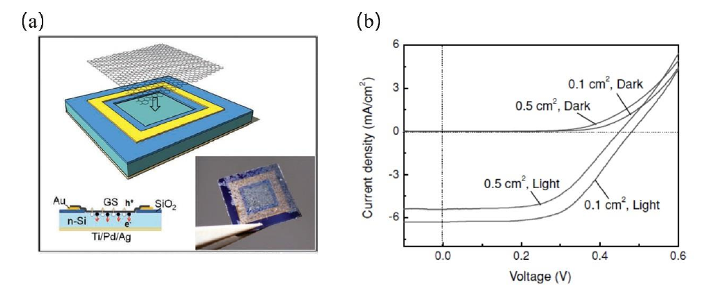
Figure 2. (a) Device schematic and physical photos of graphene/silicon heterojunction photovoltaic solar cells; (b) J-V characteristic curves of cells with different device areas under light as well as dark fields [5]
4. Nano-size organic/inorganic heterojunction solar cells
In recent years, there has been an interest in the study of nano-sized heterojunctions. These heterojunctions mainly include semiconductor-semiconductor heterojunctions, dye sensitization, polymer-metal Schottky barriers, polymer-semiconductor compounds, and polymer-semiconductor heterojunctions. The heterostructured materials easily achieve photogenerated charge separation, especially organic and inorganic semiconductor nanocomposite systems, which combine strong organic absorption and efficient charge separation with inorganic nanomaterials. These properties are widely used to improve the conversion efficiency of solar energy and the development of optoelectronic devices.
Graetzel et al.[6] proposed a solar photovoltaic cell with dye-sensitized titanium dioxide nano-films as photoanodes, which achieved a photovoltaic conversion efficiency of 10% under simulated daylight [7]. Murakoshi et al. established a solid-state photovoltaic cell using a conductive polymer, polypyrrole, synthesized on the surface of titanium dioxide nanoparticles as a conduction medium for charge transport between positive and negative electrodes [8]. Graetzel et al. also proposed an organic cavity-conducting material instead of liquid electrolyte and combined it with a titanium dioxide nanofilm with adsorbed dye to make a solid-state photovoltaic cell with a monochromatic photovoltaic efficiency of 33%[9]. In addition, Schoen et al. reported that the photoelectric conversion efficiency can be improved by molecular doping of organic materials in organic photodiodes[10].
In the research of Liu et al. [11], the composite film heterojunctions of 1,4-bis(ferrocenylthiophene) and tin dioxide nanoparticles were prepared using the LB technique. The film-forming properties of the nano-stannous heterojunction and tin dioxide were characterized by AFM and XRD, and the optical absorption and photovoltaic properties were investigated by UV-visible absorption spectroscopy and surface photovoltage spectroscopy. The photovoltaic response of the composite film heterojunction was found to be very good in the UV-Vis region.
5. Inorganic/organic heterojunction solar cells
Much progress has also been made in the study of inorganic heterojunction photovoltaics. Starting from binary inorganic compounds, more inorganic materials have been applied to heterojunction photovoltaics.
For example, ZnO is an intrinsic n-type semiconductor with a band gap of 3.37 eV. The exciton binding energy is as high as 60 meV, and it has good light transmission in the UV and visible regions and high chemical and thermal stability. Because of these properties, ZnO has a high potential for use in UV photodetectors, solar cells, and other optoelectronic devices [12]. So far, it has been difficult to obtain p-type ZnO materials that can be used at device assembly level (p-type ZnO materials for device assembly level), thus limiting the availability of ZnO homojunctions and the realization of customary high-performance LED devices. The realization of high-performance light-emitting diode devices is limited by the availability of p-type ZnO materials for device assembly. However, due to its high transmittance in the visible solar range, ZnO has been widely applied to the assembly of solar cell devices in recent years.
Cu2O is another important p-type direct bandgap oxide semiconductor material with a bandgap of 2.1 eV, which is abundant in nature and nontoxic to humans. In addition, Cu2O has a high absorption coefficient for visible light and a few carrier diffusion lengths suitable for solar cell absorber layers [13, 14]. Therefore, Cu2O is very suitable for the preparation of solar cells, and the theoretical efficiency of solar cells can reach more than 20%. However, n-type doping of Cu2O is difficult to achieve, and so far, the efforts to obtain Cu2O homojunction solar cells by n-type doping have not been successful.
Therefore, a better solution to combine the characteristics of ZnO and Cu2O for solar cell assembly is to use ZnO/Cu2O heterojunctions. Studies have shown that ZnO and Cu2O form heterojunctions with a small difference in conduction band energy levels, which has attracted attention [15, 16]. In 2000, J. Lee et al. [15] did a preliminary study on the electrochemical preparation of Cu2O and ZnO. In 2007, B. Pradhan et al. [16] used a chemical method to synthesize vertically oriented B. Pradhan et al. In 2007, T. J. Hsueh et al. [17] used magnetron sputtering to sputter a layer of ZnO film on glass and then grow a layer of ZnO nanowires. The ZnO nanowires were further sputtered with a layer of Cu2O, and the Cu2O-coated ZnO heterojunction solar cells were prepared by magnetron sputtering, and their performance was improved. In 2008, S. S. Jeong et al. [18] prepared ZnO/Cu2O solar cells by electrodeposition, and the efficiency was only 0.41%. In 2010, the paper [19] used an electrochemical method to reproduce the ZnO/Cu2O solar cell with an efficiency of only 0.41%. In 2010, the literature [19] reproduced the work of T. J. Hsueh et al. [18] by an electrochemical method, and the efficiency was improved to 0. 88%. In 2010, the literature [19] used electrochemical methods to reproduce the work of T. J. Hsueh et al. [17], and the efficiency was improved to 0.88%. However, the current conversion efficiency of Cu2O solar cells is far below the theoretical limit of 33% proposed by Shockley-Queisser, and more in-depth research is needed.
6. Conclusion
The above is a general survey of heterojunction photovoltaic studies in different directions. It can be seen that most of the new heterojunction photovoltaic materials examined in this paper do not achieve very high photovoltaic conversion efficiencies. For heterojunction photovoltaics prepared by different kinds of metal oxide inorganic materials, in the pursuit of the convenience of material preparation at the same time, the photoelectric conversion efficiency is very significantly reduced. It is not even possible to reach the photovoltaic conversion efficiency based on crystalline silicon and non-crystalline silicon for general commercial applications (the photovoltaic conversion efficiency of mass-produced cells is around 23%), not to mention the critical threshold of 33% conversion proposed by the SQ limit.
The only exception to the above presentation is the photovoltaic conversion efficiency of organic/inorganic heterojunction photovoltaics in monochromatic light from Graetzel et al., which is very close to the SQ limit. This may mean that in the current heterojunction photovoltaic research environment, new types of heterojunction photovoltaics that can replace crystalline silicon and non-crystalline silicon configurations are more likely to be dye-sensitized heterojunction cells that fully justify organic/inorganic heterojunctions.
The shortcoming of the study presented in this paper is that it does not cover all types of heterojunction photovoltaic cells, so it is likely that there is another heterostructure formation method that can completely break the Shockley-Queisser limit. This paper does not discuss in detail the functional implications of various heterojunction fabrication methods, thus limiting the study to existing types of heterojunction photovoltaics rather than establishing an idealized heterojunction PV cell fabrication method and structural model.
All in all, heterojunction PV still holds great potential in the context of today's widespread commercialization. Further research based on organic-inorganic heterojunctions will open up new possibilities for commercial applications in the future.
References
[1]. LI Z P,SHEN W Z. High efficiency hit solar cell assembly and its application[J]. Shanghai energy conservation, 2015(1): 41-45.
[2]. Biswas, Kwon, Soukoulis. Mechanism for the Staebler-Wronski effect in a-Si:H.[J]. Physical review. B, Condensed matter,1991,44(7).
[3]. Li, X. S.; Cai, W. W.; An, J.; Kim, S.; Nah, J.; Yang, D. X.; Piner, R.; Velamakanni, A.; Jung, I.; Tutuc, E.; Banerjee, S. K.; Colombo, L.; Ruoff, R. S. Large-Area Synthesis of High-Quality and Uniform Graphene Films on Copper Foils. Science 2009, 324, 1312-1314.
[4]. Nair, R. R.; Blake, P.; Grigorenko, A. N.; Novoselov, K. S.; Booth, T. J.; Stauber, T.; Peres, N. M. R.; Geim, A. K. Fine structure constant defines visual transparency of graphene. Science 2008, 320, 1308.
[5]. Kobayashi, T.; Bando, M.; Kimura, N.; Shimizu, K.; Kadono, K.; Umezu, N.; Miyahara, K.; Hayazaki, S.; Nagai, S.; Mizuguchi, Y. Production of a 100-m-long high-quality graphene transparent conductive film by roll-to-roll chemical vapor deposition and transfer process. Appl. Phys. Lett. 2013, 102, 023112.
[6]. O’Regan, B. : Graetze1, M. Nature, 1991, 353: 737
[7]. Nazeeruddin, M. K. : Kay, A. : Rodicio, I. : Humphry. Baker, R. : Mue11er, E. : Liska, P. : V1achopo1ous, N. : Gratze1, M.J. Am. Ceram. soc., l993, ll5: 6382
[8]. Murakoshi, K.: Kogure, R.: wada, Y. : Yanagida, s. Chem.Lell., l997, (5) : 471
[9]. Bach, U. : Lupo, D. : Comte, P. : Moser, J. E. : Weissoetel, F.: salbeck, J. : spreitzer, H.: Graetzel, M. Nature, l998, 395: 583
[10]. Schoen, J. H. : Kloc, Ch. : Bucher, E. : Bat1ogg, B. Nature, 2000, 403: 408
[11]. Liu, X; Zhang, Z; Zhang, X; Cheng, K; Huang, Y; Wang D; Du, Z. Photovoltaic properties of 1,4-bisferrocenyl thiophene/nanotin dioxide heterojunction[J]. Journal of Physical Chemistry,2004(09):1167-1171.
[12]. Cao B Q,Matsumoto T, Matsumoto M, et al. ZnO nanowalls grown with high-pressure PLD and their application as field emitters and UV detectors [J] . Journal of Physics Chemistry C,2009,113 (25) : 10975—10980.
[13]. Golden T D, Shumsky M G, Zhou Y, et al. Electrochemical deposition of copper(I) Oxide films[J]. Chemistry of Materials,1996,8(10) : 2499—2504.
[14]. Tanaka H,Shimakawa T,Miyata T,et al. Electrical and optical properties of TCO-Cu2O heterojunction devices[J]. Thin Solid Films,2004,469-470(1-2) : 80—85.
[15]. Lee J,Tak Y. Selective electrodeposition of ZnO onto Cu2O[J]. Electrochemistry Communications,2000, 2(11) : 765—768.
[16]. Pradhan B,Batabyal S K,Pal A J. Vertically aligned ZnO nanowire arrays in Rose Bengal-based dye- sensitized solar cells[J]. Solar Energy Materials and Solar Cells,2007,91(9) : 769—773.
[17]. Hsueh T J,Hsu C L,Chang S J,et al. Cu2O/n-ZnO nanowire solar cells on ZnO: Ga /glass templates[J]. Scripta Materialia,2007,57(1) : 53—56.
[18]. Jeong S S,Mittiga A,Salza E,et al. Electrodeposited ZnO/Cu2Oheterojunction solar cells[J]. Electrochimica Acta,2008,53(5) : 2226—2231.
[19]. Cui J B,Gibson U J. A simple two-step electrodeposition of Cu2O/ZnO nanopillar solar cells[J]. Journal of Physics Chemistry C,2010,114(14) : 6408—6412.
Cite this article
Bin,Z. (2023). A comparison between the mainstream heterojunction PV studies. Applied and Computational Engineering,7,29-34.
Data availability
The datasets used and/or analyzed during the current study will be available from the authors upon reasonable request.
Disclaimer/Publisher's Note
The statements, opinions and data contained in all publications are solely those of the individual author(s) and contributor(s) and not of EWA Publishing and/or the editor(s). EWA Publishing and/or the editor(s) disclaim responsibility for any injury to people or property resulting from any ideas, methods, instructions or products referred to in the content.
About volume
Volume title: Proceedings of the 3rd International Conference on Materials Chemistry and Environmental Engineering (CONF-MCEE 2023), Part II
© 2024 by the author(s). Licensee EWA Publishing, Oxford, UK. This article is an open access article distributed under the terms and
conditions of the Creative Commons Attribution (CC BY) license. Authors who
publish this series agree to the following terms:
1. Authors retain copyright and grant the series right of first publication with the work simultaneously licensed under a Creative Commons
Attribution License that allows others to share the work with an acknowledgment of the work's authorship and initial publication in this
series.
2. Authors are able to enter into separate, additional contractual arrangements for the non-exclusive distribution of the series's published
version of the work (e.g., post it to an institutional repository or publish it in a book), with an acknowledgment of its initial
publication in this series.
3. Authors are permitted and encouraged to post their work online (e.g., in institutional repositories or on their website) prior to and
during the submission process, as it can lead to productive exchanges, as well as earlier and greater citation of published work (See
Open access policy for details).
References
[1]. LI Z P,SHEN W Z. High efficiency hit solar cell assembly and its application[J]. Shanghai energy conservation, 2015(1): 41-45.
[2]. Biswas, Kwon, Soukoulis. Mechanism for the Staebler-Wronski effect in a-Si:H.[J]. Physical review. B, Condensed matter,1991,44(7).
[3]. Li, X. S.; Cai, W. W.; An, J.; Kim, S.; Nah, J.; Yang, D. X.; Piner, R.; Velamakanni, A.; Jung, I.; Tutuc, E.; Banerjee, S. K.; Colombo, L.; Ruoff, R. S. Large-Area Synthesis of High-Quality and Uniform Graphene Films on Copper Foils. Science 2009, 324, 1312-1314.
[4]. Nair, R. R.; Blake, P.; Grigorenko, A. N.; Novoselov, K. S.; Booth, T. J.; Stauber, T.; Peres, N. M. R.; Geim, A. K. Fine structure constant defines visual transparency of graphene. Science 2008, 320, 1308.
[5]. Kobayashi, T.; Bando, M.; Kimura, N.; Shimizu, K.; Kadono, K.; Umezu, N.; Miyahara, K.; Hayazaki, S.; Nagai, S.; Mizuguchi, Y. Production of a 100-m-long high-quality graphene transparent conductive film by roll-to-roll chemical vapor deposition and transfer process. Appl. Phys. Lett. 2013, 102, 023112.
[6]. O’Regan, B. : Graetze1, M. Nature, 1991, 353: 737
[7]. Nazeeruddin, M. K. : Kay, A. : Rodicio, I. : Humphry. Baker, R. : Mue11er, E. : Liska, P. : V1achopo1ous, N. : Gratze1, M.J. Am. Ceram. soc., l993, ll5: 6382
[8]. Murakoshi, K.: Kogure, R.: wada, Y. : Yanagida, s. Chem.Lell., l997, (5) : 471
[9]. Bach, U. : Lupo, D. : Comte, P. : Moser, J. E. : Weissoetel, F.: salbeck, J. : spreitzer, H.: Graetzel, M. Nature, l998, 395: 583
[10]. Schoen, J. H. : Kloc, Ch. : Bucher, E. : Bat1ogg, B. Nature, 2000, 403: 408
[11]. Liu, X; Zhang, Z; Zhang, X; Cheng, K; Huang, Y; Wang D; Du, Z. Photovoltaic properties of 1,4-bisferrocenyl thiophene/nanotin dioxide heterojunction[J]. Journal of Physical Chemistry,2004(09):1167-1171.
[12]. Cao B Q,Matsumoto T, Matsumoto M, et al. ZnO nanowalls grown with high-pressure PLD and their application as field emitters and UV detectors [J] . Journal of Physics Chemistry C,2009,113 (25) : 10975—10980.
[13]. Golden T D, Shumsky M G, Zhou Y, et al. Electrochemical deposition of copper(I) Oxide films[J]. Chemistry of Materials,1996,8(10) : 2499—2504.
[14]. Tanaka H,Shimakawa T,Miyata T,et al. Electrical and optical properties of TCO-Cu2O heterojunction devices[J]. Thin Solid Films,2004,469-470(1-2) : 80—85.
[15]. Lee J,Tak Y. Selective electrodeposition of ZnO onto Cu2O[J]. Electrochemistry Communications,2000, 2(11) : 765—768.
[16]. Pradhan B,Batabyal S K,Pal A J. Vertically aligned ZnO nanowire arrays in Rose Bengal-based dye- sensitized solar cells[J]. Solar Energy Materials and Solar Cells,2007,91(9) : 769—773.
[17]. Hsueh T J,Hsu C L,Chang S J,et al. Cu2O/n-ZnO nanowire solar cells on ZnO: Ga /glass templates[J]. Scripta Materialia,2007,57(1) : 53—56.
[18]. Jeong S S,Mittiga A,Salza E,et al. Electrodeposited ZnO/Cu2Oheterojunction solar cells[J]. Electrochimica Acta,2008,53(5) : 2226—2231.
[19]. Cui J B,Gibson U J. A simple two-step electrodeposition of Cu2O/ZnO nanopillar solar cells[J]. Journal of Physics Chemistry C,2010,114(14) : 6408—6412.