


1. Introduction
With the advancement of technology, VR/AR has emerged as one of the key development trends. In 2014, Google made its entry into the VR domain by launching its inaugural VR product, the Google Cardboard [1]. In 2021, Facebook announced the metaverse project and change the name to Meta. Meta has emphasized that the metaverse will play an important role in the future. According to [2], in 2025, VR/AR industry will reach 80 billion dollar of business.
There are lots of research showing VR/AR can be use in various industry, it can improve medical treatment level by using a VR device in surgery, it provides better experience and better understanding of knowledge to students in education, and VR/AR can provide users with the most immersive gaming experience.
However, the VR/AR today cannot deliver competitive user experience due to the hardware capability. VR/AR needs a high resolution and high FPS to provide users a good experience which requires a relatively high power graphic processor, but the edge device can’t handle this amount of data and calculations. There are 2 possible solutions for this scenario, firstly, we can use a high performance processor like GPU to process the data, but in real life, it is impossible to attach a GPU on a VR/AR headsets, the reason of that is a GPU is a relatively high power consumption module, which means it produces large amount of heat and also requires very powerful battery in the headset, therefore, this possible solution is not likely to be applied in industry. Secondly, problems from the first solution can be solved by using a GPU from the host (personal computer) and as long as we transmit the data to the edge device, We can achieve building a VR/AR device in high resolution and it provides good experience to the user. However, in a real time system, take Oculus quest 2 as an example, it needs a transmission speed of 1.6GB/s for 1 frame with WIFI. It is hard to provide such large bandwidth in wireless protocol, the bandwidth of 5G is approximately 1Gb/s [3] and the bandwidth of WIFI6 is about , even with 5G or WIFI6, the bandwidth of the communication protocols nowadays are not able to provide 1.6GB/s bandwidth. Compression algorithm may not work well in a real time system because of the latency with cause a bad experience. This issue can be solved by connecting the PC and the edge device with a HDMI/DP cable.
This paper aims to utilize FPGA technology to develop a CNN accelerator for DLSS (Deep Learning Super Sampling) in order to provide a high-resolution and high-frame-rate experience in VR/AR environments,
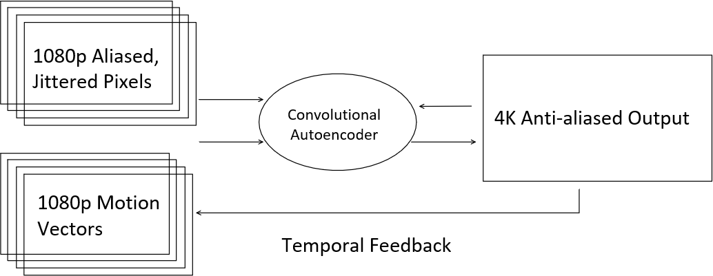
Figure 1. Process of deep learning super sampling.
while employing a wireless protocol. The initial step in- volves measuring the time difference between generating normal 1080p frames and generating 1080p to 4K frames using DLSS like methodology. Subsequently, an FPGA based accelerator with equivalent computational power to the DLSS-based CNN is constructed to evaluate power consumption, latency, image quality, and other factors impacting the user experience. Additionally, machine learning techniques are employed to compress video in real-time during the rendering process.
2. Background
2.1. Virtual Reality(VR) and Augmented Reality(AR)
VR/AR is a popular topic in lot of areas, for example, many industries have projects in form of VR/AR, researches about VR/AR also illustrate how topical it is. Users carry an edge, it can be a smart phone or a headset. By using a VR/AR device, users can see the a virtual environment surrounding. However, since the edge devices have very limited calculation power, users don’t have the same experience in terms of display quality as a personal computer while using a wireless protocol. This problem can be solved by using a HDMI cable to transmit data from GPU to the edge device, but cables will lower the experience in VR/AR.
2.2. Deep Learning Super Sampling(DLSS)
DLSS generates few frames in lower quality and finally combine to one frame. For example if the target resolution is 4K, then DLSS can generate 4 1080p frames, then a pipeline method is applied to combine the frames to one 4K frame using a convolutional autoencoder. Technically, we can use GPU from our host to generate frames in lower quality, then use a wireless protocol to transmit data to the edge devices since the amount of data is reduced, finally use a CNN to combined the frames to a higher resolution frame. The propose of this technique in this paper is to cut the bandwidth requirement to meet the 5G/WIFI6 bandwidth.
2.3. Systolic array
Systolic array is an architecture that was introduced in the 1980s. This architecture is often used for repetitive computational processes, and instead of using instruction, systolic array uses data flow to control the operation. In a systolic array, input data is usually pushed into a shift register, and each register has a corresponding operation. When an input data is pushed into the shift register, the output will be obtained after a series of data flows and calculations.
In this paper, we used 2D systolic array to achieve the flow of data by using vertical and horizontal register to complete the computation of convolution.
3. Related work
3.1. Rendering multi-party mobile augmented reality from edge
[4] The author implemented VR rendering in an edge device, they designed an AR application and rendered images of a virtual earth using the edge device. Base on the data, the performance is relatively not high because of the edge device is not powerful enough.
3.2. QARC: video quality aware rate control for real- time video streaming via deep reinforcement learning
[5] This paper presents a rate control algorithm called QARC, which aims to obtain higher quality images at the lowest possible rate and transmission delay. QARC trains a neural network by using deep reinforcement learning( DRL) and selects the bitrate based on the previous video quality and network status.
4. Architecture
4.1. Design Details
Our goal is to develop an FPGA accelerator capable of executing CNN calculations. This will enable us to gather data on the power and area utilization of the accelerator. With this information, we can assess the feasibility of deploying the accelerator in real-world practical applications. The top level of the entire design is shown in Figure 2, the accelerator is attached to the memory bus as a core processor on FPGA
The entire calculation module consists of three sub- modules, and these three modules are mainly responsible for completing convolution. The top module will add the results obtained by the three sub-modules to get the result of the final output channel. In addition, the top module will also output the addresses of the pixels and filter data that need to be loaded to the sub-module.
Each submodule functions identically. In practical scenarios, a combined total of 3x13 pixel data sets will be loaded into the Processing Element (PE). Subsequently, the filter data will be sequentially fed into the PE via a shift register, facilitating the required multiplications at their respective positions (refer to Figure 3). This process involves pushing filter data into the shift register every three or five clock cycles, depending on the filter size. With each submodule comprising 13 columns, it takes 13 clock cycles for a majority of PEs within the computation module to engage in simultaneous computation. This configuration establishes an efficient computational pattern.
Filter data will undergo a continuous and cyclic push into the shift register. Upon the completion of a full cycle of pushing filter data, it signifies the computation of pixel data for those three rows is finished. Consequently, when the last filter data is pushed into the shift register, the subsequent cycle will involve loading new pixel data into the column where calculations have already been completed. To illustrate, if we assume the existence of 10 output channels, the moment the tenth filter is pushed into the shift register, the first filter will follow suit, and the PE will receive new pixel data.
In our specific design, each filter comprises 8 bits of data. Since every sub-module encompasses three rows of pixels, there exists a total of 24 bits of input within each sub-module. The uppermost module allocates these 24 bits across each row.
The design maintains a fixed sequence for filter appearance and data arrangement. As a result, when loading new pixel data, the vertical shift register is employed. This causes the new pixel data to load into the bottom row, simultaneously shifting the original pixel data upwards by one step.
To enhance efficiency, we aim to maximize the work- load of each computing unit within a single clock cycle. Consequently, we need to allocate data simultaneously to each computing unit. In order to achieve this objective, the filter data should be evenly divided among all the computing units. After each computing unit completes the calculation of all the allocated data, the new uncalculated filter data will be read and calculated. When a computing unit completes 70 readings and calculations, the result of the convolution of the first layer will also be obtained.
In this project, we can take the size of 2K to tolerant multiply CNN configuration and double buffering, so as to achieve efficient operation of reading data while computing. In addition, each computing sub-unit also needs an extra SRAM to store the next row of pixel data. Because the pixel data does not need to be reused and the reading cycle is shorter than that of the filter data, we do not need to allocate additional SRAM to each computing sub-unit to complete the operation of computing while reading the pixel data. As we mentioned in above, each calculation module has 3 sub-modules. Therefore, we allocated a total of 9 SRAMs to each calculation module.
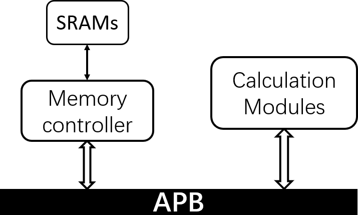
Figure 2. High level modules.
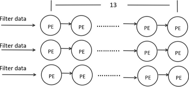
Figure 3. Sub-module design.
5. Methodology
5.1. Determine the number of computing units
By estimating the amount of calculation, we can determine the number of computing units are needed to complete the reconstruction of a 1080P image.
We perform an estimation of the overall computation load of the CNN model in [5]. To illustrate, let’s consider the first layer with 3 input channels, 64 filters, an input image size of 1076x1916 pixels, and a filter dimension of 5 5. As a result, we calculate that the first layer necessitates accomplishing approximately 5.9371012calculations.
Importantly, following the completion of Convolution for the first three layers, the Neural Network will apply maxpooling to the output of each layer. For instance,
upon the completion of Convolution for the first layer, the output image dimensions would be 1076x1916. After applying maxpooling, the dimensions would be reduced to 538 958. This transformed output serves as the input for the second layer.
If we want to calculate the number of required computing units, we also need to know the computing power of the computing unit. There are 13*9 ALUs in the design of each computing unit mentioned above. If we assume that the input filter is 3*3, it can be concluded that the computing unit can perform calculations on 4 input filters at the same time, and thus the calculation amount that can be completed by one computing unit in one clock cycle is: filter size = 108. we use a clock with a frequency of 1GHz to synthesize, so the computing unit can complete 1.08*1011 operations in 1 second. By dividing the total calculation amount of the 4 layers by the calculation amount that the computing unit can complete in 1 second, we get the total number of computing units required to complete the operation. Based on the earlier calculation to , where we determined a requirement of approximately 70 calculation modules, dividing the filter data into 70 equal parts would result in a size of 686B for each partition.
5.2. Power and area of computing units
We implement the computing units in System Verilog to estimate the power and area of the design. Then we simulate them with testbench to verify the functionality of the computing units and synthesis the design with 130nm technology. Once we determine the number of calculation modules needed to achieve a frame rate of 60FPS, we can derive the total power and area to keep the throughput of our design goal.
We ascertain the necessary size of Static Random Access Memory (SRAM) for each computing unit. In our architectural blueprint, SRAM serves as storage for both filter data and the subsequent pixel row among the three consecutive rows. Hence, our initial task involves identifying the predominant layer dictating the SRAM size, given that our SRAM dimensions are typically determined by the data requiring the greatest storage capacity. In our specific design, it becomes evident that the primary convolutional layer holds dominance, amounting to 48,000 bytes for filter data.
We use Cacti [6] to estimate the power and area of SRAMs in 65nm technology. Each sub-module has a 24- bit input, so we choose to use SRAM with a block size of 24, because each computing unit can complete the calculation of 3 input channels, and the input of each channel is 8 bits of filter data and pixel data.
6. Results
By changing the cache size and block size, we got some simulation parameters about the power and area of SRAM, and we recorded it in the table II. By simulating the power and area of SRAMs with cache size = 2048, block size = 2, we get the result that SRAMs occupy a total of 5.076w of energy and an area of 41.766mm2.
Analyzing measurement data from Cacti [6] reveals that simulating SRAM using a cache size of 2048 shows that the Block Size has minimal to no impact on Power and Area. This finding is particularly evident when the block size is set to 24 and the cache size remains at 2048. Under these conditions, the energy consumption per read is approximately 0.00805702nJ, and the corresponding Area is approximately 0.0662951mm2.
Table 1. CNN-calculations.
layer 1 | layer 2 | layer 3 | layer 4 | |
#calculations | 5.937*1012 | 1.133*1012 | 2.801*1011 | 3.419*1010 |
I simulated the power and area of a single computing unit, each occupy 101.296 mw of power and 1447353 um2 of area. The total power and area of the acclerator can be obtained by calculating the number of computing units required for different CNN models, as shown in Figures 4 and 5.
I chose to use a CNN model with 64 filters and10 input channels, which requires approximately 70 computational units. With this setting, the total power consumption of the accelerator is 20.968 W and the area is 299.603 mm2.
The power and area is significant as an accelerator. However, as we are using 130nm technology. The power and area will be much smaller with technology scaling.
Table 2. Sram power and area, cache size = 2048, block size = 24.
power(w) | Area(mm2) | |
One SRAM | 8.057*10−3 | 0.0662951 |
SRAM in total | 5.076 | 41.766 |
Accelerator | 20.968272 | 299.602071 |
SRAM and accelerator | 26.044 | 341.368 |
7. Conclusion
In this work, we present a machine learning-based latency-sensitive super sampling hardware acclerator for
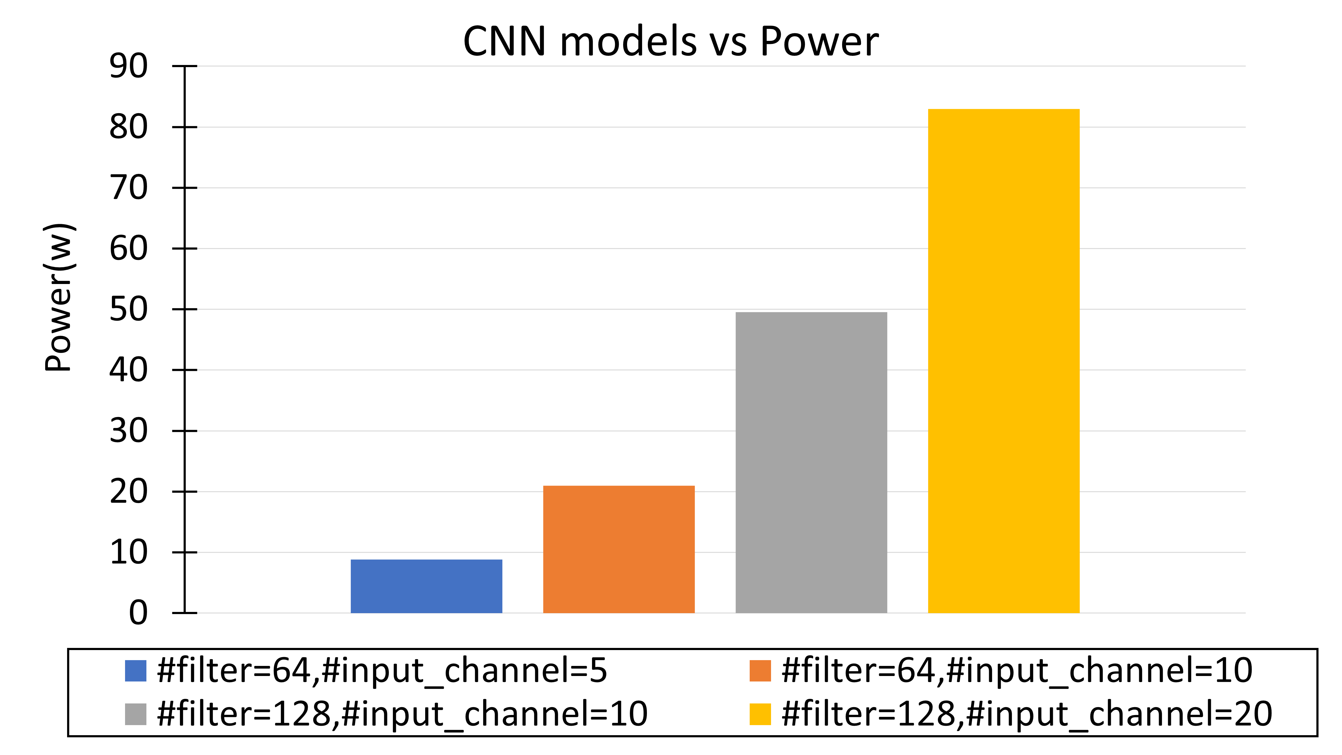
Figure 4. Accelerator power for various CNN model.
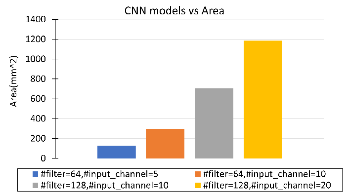
Figure 5. Accelerator area for various CNN model.
VR/AR devices that dramatically reduces the bandwidth required to transmit frames to VR/AR, and explore the feasibility of the accelerator in reality by calculating the number of computing units required for various CNN models to estimate the overall power consumption and area of the accelerator.
Reducing bandwidth means that people can have a better experience on VR/AR, and usage scenarios that sacrifice the image quality or wireless functionality will be addressed.
In this paper, the experimental results show that it is possible to solve such problems, and although there is a problem of excessive power and area of the final hardware, the power and area would be greatly reduced if a more advanced technology is used instead of the 130nm technology used in this paper.
References
[1]. Google, “Googlecardboard,” Availableat https://vr.google.com/cardboard/ (2016).
[2]. G. Sachs, “The real deal with virtual and augmented reality,” Available at http://www.goldmansachs.com/ our- thinking/pages/virtual-and-augmented-reality.html (2016).
[3]. Y. Ghazaoui, A. E. Alami, M. E. Ghzaoui, S. Das, D. Barad, and S. Mohapatra, “Millimeter wave antenna with enhanced bandwidth for 5g wireless application,” Journal of Instrumentation, vol. 15, no. 01, p. T01003, jan 2020. [Online]. Available: https://dx.doi.org/10.1088/1748-0221/15/01/T01003
[4]. L. Zhang, A. Sun, R. Shea, J. Liu, and M. Zhang, “Rendering multi-party mobile augmented reality from edge,” p. 67–72, 2019. [Online]. Available: https://doi.org/10.1145/3304112.3325612
[5]. T. Huang, R.-X. Zhang, C. Zhou, and L. Sun, “Qarc: Video quality aware rate control for real-time video streaming based on deep reinforcement learning,” p. 1208–1216, 2018. [Online]. Available: https://doi.org/10.1145/3240508.3240545
[6]. N. Muralimanohar, R. Balasubramonian, and N. P. Jouppi, “Cacti 6.0: A tool to model large caches,” HP laboratories, vol. 27, p. 28, 2009.
Cite this article
Mei,L. (2024). FPGA accelerator for wireless AR/VR display. Applied and Computational Engineering,34,57-63.
Data availability
The datasets used and/or analyzed during the current study will be available from the authors upon reasonable request.
Disclaimer/Publisher's Note
The statements, opinions and data contained in all publications are solely those of the individual author(s) and contributor(s) and not of EWA Publishing and/or the editor(s). EWA Publishing and/or the editor(s) disclaim responsibility for any injury to people or property resulting from any ideas, methods, instructions or products referred to in the content.
About volume
Volume title: Proceedings of the 2023 International Conference on Machine Learning and Automation
© 2024 by the author(s). Licensee EWA Publishing, Oxford, UK. This article is an open access article distributed under the terms and
conditions of the Creative Commons Attribution (CC BY) license. Authors who
publish this series agree to the following terms:
1. Authors retain copyright and grant the series right of first publication with the work simultaneously licensed under a Creative Commons
Attribution License that allows others to share the work with an acknowledgment of the work's authorship and initial publication in this
series.
2. Authors are able to enter into separate, additional contractual arrangements for the non-exclusive distribution of the series's published
version of the work (e.g., post it to an institutional repository or publish it in a book), with an acknowledgment of its initial
publication in this series.
3. Authors are permitted and encouraged to post their work online (e.g., in institutional repositories or on their website) prior to and
during the submission process, as it can lead to productive exchanges, as well as earlier and greater citation of published work (See
Open access policy for details).
References
[1]. Google, “Googlecardboard,” Availableat https://vr.google.com/cardboard/ (2016).
[2]. G. Sachs, “The real deal with virtual and augmented reality,” Available at http://www.goldmansachs.com/ our- thinking/pages/virtual-and-augmented-reality.html (2016).
[3]. Y. Ghazaoui, A. E. Alami, M. E. Ghzaoui, S. Das, D. Barad, and S. Mohapatra, “Millimeter wave antenna with enhanced bandwidth for 5g wireless application,” Journal of Instrumentation, vol. 15, no. 01, p. T01003, jan 2020. [Online]. Available: https://dx.doi.org/10.1088/1748-0221/15/01/T01003
[4]. L. Zhang, A. Sun, R. Shea, J. Liu, and M. Zhang, “Rendering multi-party mobile augmented reality from edge,” p. 67–72, 2019. [Online]. Available: https://doi.org/10.1145/3304112.3325612
[5]. T. Huang, R.-X. Zhang, C. Zhou, and L. Sun, “Qarc: Video quality aware rate control for real-time video streaming based on deep reinforcement learning,” p. 1208–1216, 2018. [Online]. Available: https://doi.org/10.1145/3240508.3240545
[6]. N. Muralimanohar, R. Balasubramonian, and N. P. Jouppi, “Cacti 6.0: A tool to model large caches,” HP laboratories, vol. 27, p. 28, 2009.