


1. Introduction
The 21st century is the age of intelligent living. The Internet of Things is getting better every day. Pervasive and edge computing applications are becoming more and more widespread. The construction of smart cities continues to advance. In the context of the times, the process of communication between various devices and modules grows to an unprecedented scale. However, the communication and control between the sensor devices and the host controller as well as the devices in various application scenarios rely on various interfaces. With the continuous development of the electronics industry, the complexity of sensor devices and the growing volume of transmitted data have higher requirements for communication than ever before. Bus-based communication becomes the primary means of transmitting control information and data [1].
SPI is a standard for serial transmission introduced by Motorola in the United States. It is a high-speed, full-duplex, synchronous communication bus that supports serial data exchange between master and slave devices. SPI is a more efficient data transfer protocol, with only four pins in the chip for control and data transfer, simple structure, and save PCB space. SPI serial communication bus is increasingly integrated into chips as a communication interface due to its simple and easy-to-use structure and fast communication speed [2,3]. The SPI bus hardware is very powerful and is often used for serial communication between microcontroller units (MCU) and various peripheral devices [4,5].SPI is also widely used in power equipment, such as smart microgrids and various types of sensors [6,7], to provide communication for the successful operation of the equipment. In the future, SPI is important for enhancing the stability of inter-device communication [8], increasing the communication rate, and strengthening data encryption and transmission security [9].
This design will implement an SPI interface based on FPGA, and complete the send and receive data test to verify the SPI interface function. The implementation process mainly contains three aspects of communication protocol analysis, interface logic analysis and design, and communication simulation and verification.
2. SPI communication protocol
2.1. SPI interface signals and system composition
The SPI interface is simple. It uses four signal lines to complete the data transfer, which are the two data receiving/transmitting pins (MISO, MOSI), the slave selection signal CS pin and the SPI's clock pin (SCK) [10]. The specific functions are described in Table 1.
Table 1. SPI interface pinout.
Signal Pin Name | functionality |
MOSI(master output and slave input) | Bidirectional Data Transfer Cable |
MISO(slave output and master input) | Bidirectional Data Transfer Cable |
CS(Slave Selection Signal) | When the SPI needs to communicate with the slave, it will set this signal to an active level. |
SCK(Serial clocks) | SPI clock with bi-directional clock edge operation for synchronized data transfer. |
SPI specifies that communication between two SPI devices must be controlled by the master device to the slave device. A typical SPI system configuration consists of at least one master, one or more slaves. The master selects the slave(s) to be communicated with and sends a synchronization clock to them via the chip select pin. They input and output data through the MOSI and MISO pins, respectively. The exchange of data between the master and the slaves is accomplished like a ring shift register. The general master-slave connection is shown in Figure 1.
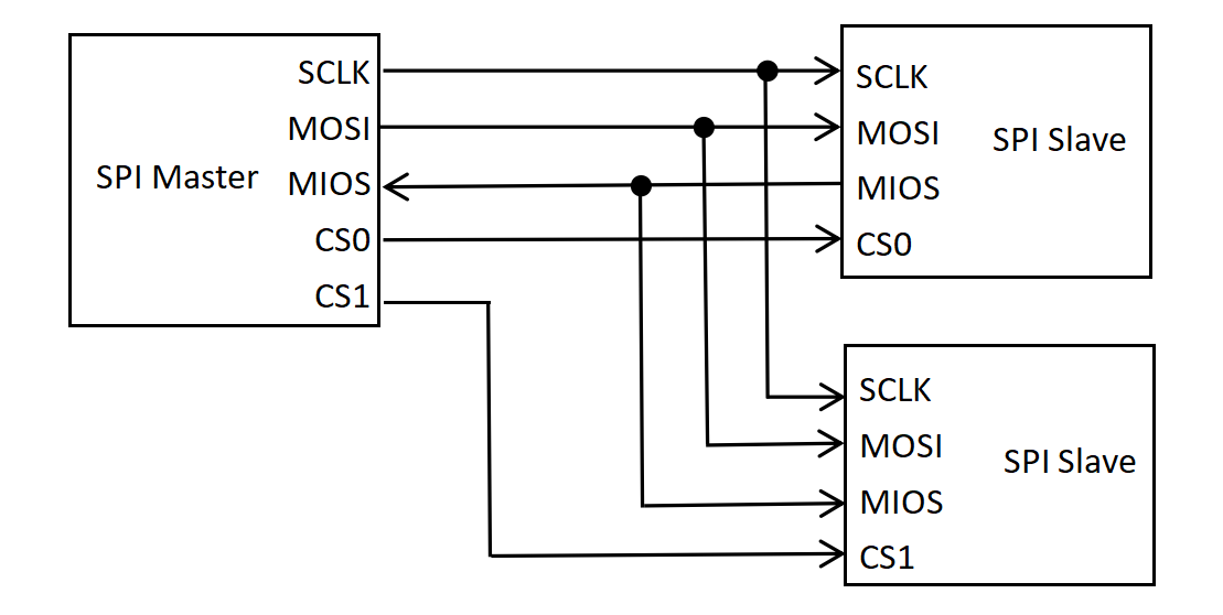
Figure 1. SPI master-slave connection method.
2.2. Operating modes of SPI
The clock mode of SPI is determined by the clock polarity CPOL and the clock phase CPHA. CPOL=0 means that the idle state of the serial synchronous clock SCK is low 0 when there is no pulse. CPOL=1 means that the idle state of the serial synchronous clock SCK is high 1 when there is no pulse,. CPHA=1 means that data is sampled on the first rising or falling edge of the serial synchronous clock SCK. CPHA=1 means that data is sampled on the second rising or falling edge of the serial synchronous clock SCK. CPHA=1 means that the data is sampled at the second rising or falling edge of the serial synchronization clock SCK. SPI0 means CPOL=0/CPHA=0. SPI1 means CPOL=0/CPHA=1. SPI2 means CPOL=1/CPHA=0. SPI3 means CPOL=1/CPHA=1. the most commonly used modes are SPI0 and SPI3. SPI can configure CPOL and CPHA according to the requirements of the peripheral devices. The clock polarity and phase of the SPI's main module and the peripheral device should be the same [11]. The four modes of operation of SPI are shown in Figure 2.
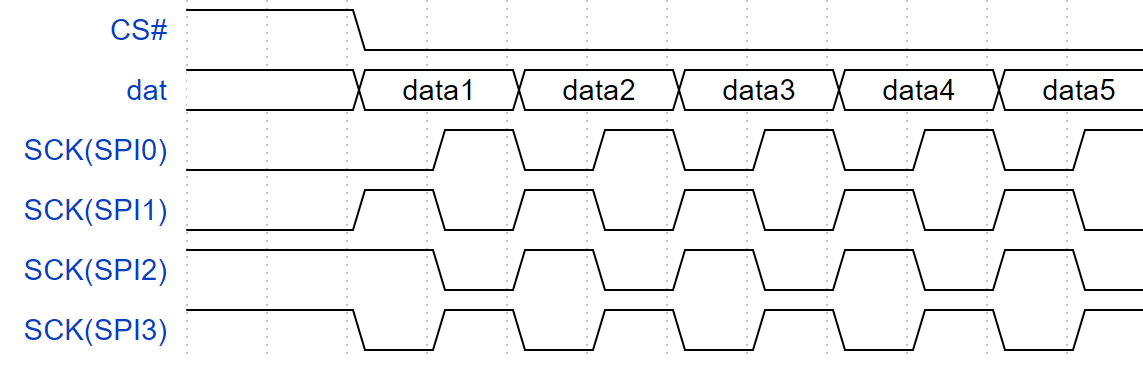
Figure 2. SPI four modes of operation.
3. Design ideas
The basic objective of this design is to implement a synchronous serial communication interface by writing Verilog code on ModelSim SE software. The experimental results are obtained by waveform observation and analysis on the software.
3.1. Basic module architecture
The SPI protocol verification module designed in this project can be roughly divided into three types of interfaces. Firstly, the system interface is responsible for transmitting the system clock signal and resetting the signal. Secondly, the configuration interface is responsible for configuring the master and slave selection, working mode, and data transmission format of the SPI interface. Thirdly, pin control interface: accountable for setting signals such as enabling the output of pins. The block diagram is shown in Figure 3.
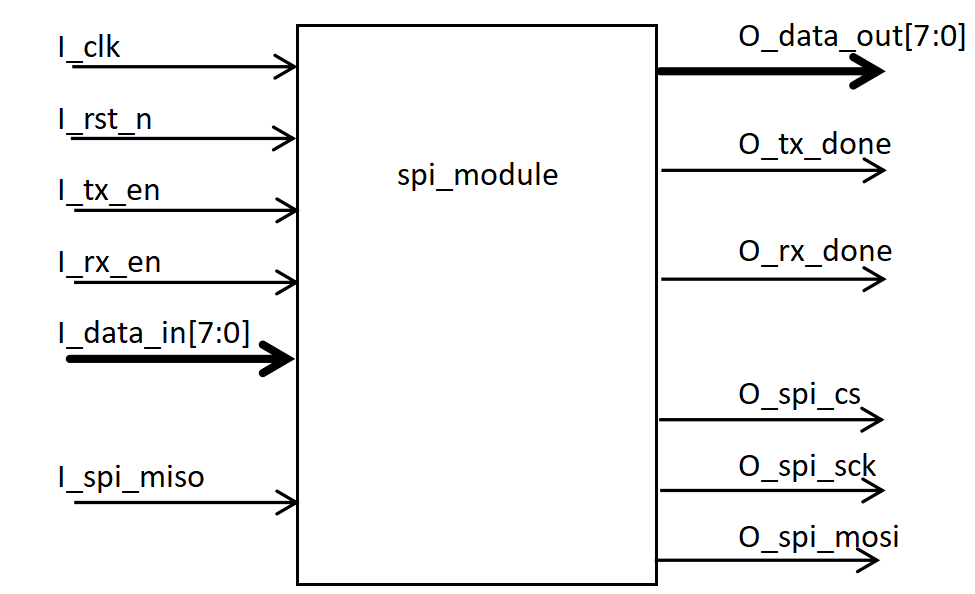
Figure 3. SPI block diagram.
The specific functions of each interface are as follows: I_clk is the system clock. I_rst_n is the system reset. I_tx_en is the enable signal for the host to send data to the slave, and the host can only send data to the slave when I_tx_en is 1. I_rx _en is the enable signal for the host to receive data from the slave, and the host can only receive data from the slave when I_rx_en is 1 I_data_in is the parallel data to be sent by the host. O_data_out is the parallel data after parallelizing the serial data received back from the slave. O_tx_done is the flag bit for the host to send data to the slave, and a high pulse will be generated after the sending is completed. O_rx_done is the flag bit for the host to receive data from the slave, and a high pulse will be generated after the receiving is completed. I_spx _en is the enable signal for the host to receive data from the slave, when I_rx_en is 1, the host can receive data from the slave. O_rx_done is a flag bit for the host to receive data from the slave, which generates a high pulse when receiving is completed. I_spi_miso, O_spi_cs, O_spi_sck, and O_spi_mosi are four wires specified by the standard SPI bus protocol.
This module is designed to use a finite state machine to implement the entire system state transition process. The signals such as clocks on which the state transitions depend are generated by the clock logic.
3.2. Transmitter module design
When the FPGA sends a byte (8-bit) of data over the SPI bus, first the FPGA sets the CS chip select signal of the selected slave to 0, indicating that it is ready to start sending data. The whole process of sending data can actually be divided into 16 states. State 0: SCK is 0, MOSI is the highest bit of the data to be sent, i.e., I_data_in[7]; State 1: SCK is 1, MOSI stays unchanged; State 2: SCK is 0, MOSI is the second highest bit of the data to be sent, i.e., I_data_in[6]; State 3: SCK is 1, MOSI stays unchanged ...... and so on. When the status number is even transmited the data sequentially from high to low until one byte of data is sent. When the status number is odd, MOSI remains unchanged. The state transfer diagram of the transmitter module is shown in Figure 4.
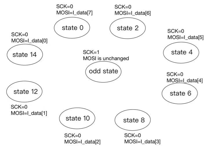
Figure 4. State transfer diagram of the sending module.
After a byte of data has been sent, a send completion flag O_tx_done is generated and the CS signal is pulled up to complete a send. By looking at the above states, it can be seen that the operations to be performed by the states with an odd number of statuses are practically the same. So when writing code, in order to streamline the code, all the states with an odd number of statuses can be integrated together.
3.3. Receiver module design
When the FPGA receives a byte (8-bit) of data via the SPI bus, first the FPGA sets the SS chip select signal to 0, indicating that it is ready to start receiving data. The whole process of receiving data can actually be divided into 16 states. Unlike the sending process, the data must be sampled right in the middle of the data in order to ensure that the received data is accurate. So each state of the receiving process performs the following operations: state 0: SCK is 0, do not latch the data on MISO; state 1: SCK is 1, latch the data on MISO, i.e. assign the data on MISO to O_data_out[7]; state 2: SCK is 0, do not latch the data on MISO; state 3: SCK is 1, latch the data on MISO that is, assign the data on MISO to O_data_out[6]. When the status number is odd the data is stored in order from high to low. No data is saved when the status number is even. The state transfer diagram of the transmitter module is shown in Figure 5.
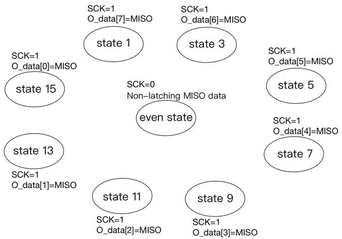
Figure 5. State transfer diagram of the receiver module.
After a byte of data has been received, a reception completion flag O_rx_done is generated and the CS signal is pulled high to complete the reception of data. By observing the above states, it can be seen that the operations to be done in the states with even numbered states are actually the same. So when writing the code, in order to streamline the code, all the states with even numbered statuses can be integrated together. This is just the opposite of the state of the sending process.
4. Simulation results analysis
In order to verify the implementation of this design, it is necessary to design the test excitation signals on ModelSim SE software and observe the resulting waveforms for data sending and receiving verification.
4.1. Transmitter module emulation
The simulated waveform of the transmitter module is obtained as shown in Figure 6.
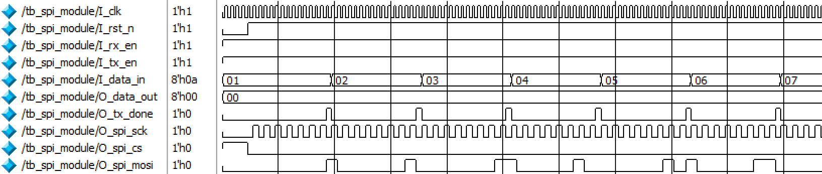
Figure 6. Simulated waveform of transmitter module.
The waveform initially pulls the send data enable signal high, indicating that it is the master sending data to the slave at this time. The chip select signal is pulled low after pulling the reset signal high to indicate the start of the data-sending process, after which the data transfer begins. When the status number increases from zero to fifteen, a send completion flag bit O_tx_done is generated and the CS signal is pulled high to complete a data transfer. During the data transfer, the counting of the status number is based on the clock signal O_spi_sck sent from the master to the slave. After eight falling edges of the clock, a one-bit transmission completion flag is generated, indicating that one data transmission is complete. the data from I_data_in is saved into O_spi_mosi.
By observing the simulated waveforms obtained from the analysis it can be seen that they are consistent with the expectations.
4.2. Receiver module simulation
The simulated waveform of the receiver module is obtained as shown in Figure 7.
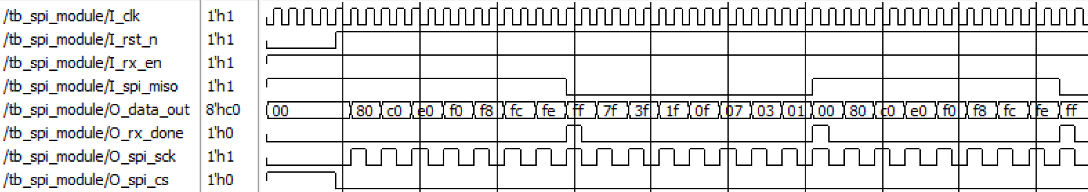
Figure 7. Receiver module simulation waveform.
The waveform initially pulls the receive data enable signal high to indicate that it is the host receiving data from the slave at this time. The chip select signal is pulled low after pulling the reset signal high to indicate the start of the data reception process, after which data transfer begins. When the status number increases from zero to fifteen, a receive completion flag bit O_rx_done is generated and the CS signal is pulled high to complete a data reception. During the data transfer, the counting of the status number is based on the clock signal O_spi_sck sent from the master to the slave. A transmission completion flag is generated after eight clock rising edges to indicate that one data transfer is complete.The data from I_spi_miso is stored in O_data_out.
From the simulation waveforms, the SPI communication protocol is well verified.The correctness of the functionality and timing of the SPI protocol transmit and receive modules was confirmed by analyzing and verifying the simulated waveforms. The transmitter module is able to accurately send one byte of data from the host to the slave and generate the transmit completion flag bit. At the same time, the receive module is able to accurately receive the data sent from the slave as expected and generate the corresponding flag bit when each data is received. This simulation verification provides a solid foundation for the subsequent hardware implementation and ensures that both the SPI transmitter and receiver modules can work stably and reliably. In practical applications, the module can meet the requirements of real-time and accuracy of data sending and receiving, and provide a guarantee for the normal operation of the system.
5. Conclusion
This paper describes the design of an FPGA based module for serial port communication. Through the SPI protocol, using a finite state machine, the SPI serial port transmit timing and receive timing are designed respectively. Through software simulation, the accuracy of data transmission is verified and the send/receive function of SPI protocol is realized. This simple and reliable design has strong operability and application value for FPGA in the development of SPI serial port communication.SPI protocol has important research significance for the future to enhance the stability of communication between devices, improve the communication rate, and strengthen data encryption and transmission security. With the continuous evolution of science and technology, SPI communication protocol will continuously adapt to new needs and provide a solid foundation for reliable communication between devices.
References
[1]. Chen M C Wei C F 2022 Asynchronous serial communication design based on Xilinx FPGA platform Computer Knowledge and Technology vol 18 no 36 p 65-67+74
[2]. Du L 2022 Design and realization of SPI interface memory chip test system. University of Electronic Science and Technology
[3]. Li L 2015 Design and verification of SPI protocol reusable IP softcore based on Verilog HDL Lanzhou University
[4]. Han Y 2017 Design and verification of SPI interface in WIFI chip Xi'an University of Electronic Science and Technology
[5]. Crepaldi M Merello A Salvo M Di 2021 A Multi-One Instruction Set Computer for Microcontroller Applications in IEEE Access vol 9 p 113454-113474
[6]. Si Y Korada N Ayyanar R Lei Q 2021 A High-Performance Communication Architecture for a Smart Micro-Grid Testbed Using Customized Edge Intelligent Devices (EIDs) With SPI and Modbus TCP/IP Communication Protocols in IEEE Open Journal of Power Electronics vol 2 p 2-17
[7]. Carimatto A 2018 Multipurpose, Fully Integrated 128 Event-Driven MD-SiPM With 512 16-Bit TDCs With 45-ps LSB and 20-ns Gating in 40-nm CMOS Technology," in IEEE Solid-State Circuits Letters vol 1 no 12 p 241-244
[8]. Lv L Han Ch H 2022 Design of wireless fire signal conversion module based on SPI bus technology. Journal of Jilin Normal College of Engineering and Technology vol 38 no 3 p 91-94
[9]. Wei X Tu Zh 2014 Design and realization of terminal security chip based on SPI interface communication. Information Security and Communication Secrecy vol 9 p 188-190
[10]. Xu Y 2020 Design and verification of high-speed SPI interface circuit Xi'an University of Electronic Science and Technology
[11]. Lin D 2012 SPI interface design based on OR1200 IP core University of Electronic Science and Technology
Cite this article
Liu,T. (2024). FPGA-based SPI serial communication. Applied and Computational Engineering,72,157-163.
Data availability
The datasets used and/or analyzed during the current study will be available from the authors upon reasonable request.
Disclaimer/Publisher's Note
The statements, opinions and data contained in all publications are solely those of the individual author(s) and contributor(s) and not of EWA Publishing and/or the editor(s). EWA Publishing and/or the editor(s) disclaim responsibility for any injury to people or property resulting from any ideas, methods, instructions or products referred to in the content.
About volume
Volume title: Proceedings of the 2nd International Conference on Functional Materials and Civil Engineering
© 2024 by the author(s). Licensee EWA Publishing, Oxford, UK. This article is an open access article distributed under the terms and
conditions of the Creative Commons Attribution (CC BY) license. Authors who
publish this series agree to the following terms:
1. Authors retain copyright and grant the series right of first publication with the work simultaneously licensed under a Creative Commons
Attribution License that allows others to share the work with an acknowledgment of the work's authorship and initial publication in this
series.
2. Authors are able to enter into separate, additional contractual arrangements for the non-exclusive distribution of the series's published
version of the work (e.g., post it to an institutional repository or publish it in a book), with an acknowledgment of its initial
publication in this series.
3. Authors are permitted and encouraged to post their work online (e.g., in institutional repositories or on their website) prior to and
during the submission process, as it can lead to productive exchanges, as well as earlier and greater citation of published work (See
Open access policy for details).
References
[1]. Chen M C Wei C F 2022 Asynchronous serial communication design based on Xilinx FPGA platform Computer Knowledge and Technology vol 18 no 36 p 65-67+74
[2]. Du L 2022 Design and realization of SPI interface memory chip test system. University of Electronic Science and Technology
[3]. Li L 2015 Design and verification of SPI protocol reusable IP softcore based on Verilog HDL Lanzhou University
[4]. Han Y 2017 Design and verification of SPI interface in WIFI chip Xi'an University of Electronic Science and Technology
[5]. Crepaldi M Merello A Salvo M Di 2021 A Multi-One Instruction Set Computer for Microcontroller Applications in IEEE Access vol 9 p 113454-113474
[6]. Si Y Korada N Ayyanar R Lei Q 2021 A High-Performance Communication Architecture for a Smart Micro-Grid Testbed Using Customized Edge Intelligent Devices (EIDs) With SPI and Modbus TCP/IP Communication Protocols in IEEE Open Journal of Power Electronics vol 2 p 2-17
[7]. Carimatto A 2018 Multipurpose, Fully Integrated 128 Event-Driven MD-SiPM With 512 16-Bit TDCs With 45-ps LSB and 20-ns Gating in 40-nm CMOS Technology," in IEEE Solid-State Circuits Letters vol 1 no 12 p 241-244
[8]. Lv L Han Ch H 2022 Design of wireless fire signal conversion module based on SPI bus technology. Journal of Jilin Normal College of Engineering and Technology vol 38 no 3 p 91-94
[9]. Wei X Tu Zh 2014 Design and realization of terminal security chip based on SPI interface communication. Information Security and Communication Secrecy vol 9 p 188-190
[10]. Xu Y 2020 Design and verification of high-speed SPI interface circuit Xi'an University of Electronic Science and Technology
[11]. Lin D 2012 SPI interface design based on OR1200 IP core University of Electronic Science and Technology