


1. Introduction
Since the dawn of the 20th century, the evolution of white light-emitting diodes (LEDs) using both organic and inorganic materials has heralded a transformative era in lighting technology, known as solid-state lighting. At the heart of this revolution lies the principle of electroluminescence - a phenomenon where electron-hole pairs, injected into a solid, recombine to emit light. This mechanism, fundamentally distinct from traditional lighting technologies, not only promises a new horizon of efficient and long-lasting light sources but also brings environmental sustainability to the forefront of modern lighting solutions.
In the realm of organic light-emitting diodes (OLEDs), we have witnessed remarkable strides in efficiency, with internal quantum efficiency (IQE) nearing the zenith of 100%.[1] Yet, a persistent bottleneck remains in the form of limited out-coupling efficiency (OCE). In conventional planar OLED structures, a significant portion of light, exceeding 80%, is lost to waveguide modes, electrode absorption, and surface plasmons.[2,3] This loss stands in stark contrast to the impressive external quantum efficiency (EQE) of red, green, and blue LEDs, which surpass 20%, 20%, and 10%, respectively.[4,5] Given that material quality has propelled IQE close to its theoretical maximum, the primary challenge now lies in enhancing the EQE by improving light out-coupling efficiency.
The quest for heightened radiation efficiency and effective external photon coupling is more than an academic pursuit; it is a crucial step towards maximizing the EQE, a vital metric for LED performance.[6,7] This paper delves into the intricacies of this challenge, employing the Transfer Matrix Method (TMM) to unravel the complex optical properties of OLEDs. Our focus is to not only understand but also enhance the way light is coupled out of these devices, thereby elevating both efficiency and the overall light-emitting impact of LED and OLED technologies.
2. Methods
The transfer matrix method (TMM) is widely used in thin-film optics to analyze the optical properties of multilayer media, playing an important role in the design and application of optical devices. The TMM uses matrix forms to describe the complex process of multiple beam interference, ultimately evaluating the modulation of electromagnetic wave amplitude and phase by the optical system through reflection and transmission coefficients. This approach provides a more intuitive understanding of the working principle and optical characteristics of the system, while clarifying the physical meaning and application of electromagnetic wave coherent superposition.
The reflection coefficient and transmission coefficient:
\( {t_{s}}=\frac{2{n_{1}}cos{{θ_{1}}}}{{n_{1}}cos{{θ_{1}}}+\frac{{μ_{r}}1}{{μ_{r}}2}{n_{2}}cos{{θ_{2}}}} \)
\( {r_{s}}=\frac{{n_{1}}cos{{θ_{1}}}-\frac{{μ_{r}}1}{{μ_{r}}2}{n_{2}}cos{{θ_{2}}}}{{n_{1}}cos{{θ_{1}}}+\frac{{μ_{r}}1}{{μ_{r}}2}{n_{2}}cos{{θ_{2}}}} \)
\( {t_{p}}=\frac{2{n_{1}}cos{{θ_{1}}}}{\frac{{μ_{1}}}{{μ_{2}}}{n_{2}}cos{{θ_{1}}}+{n_{1}}cos{{θ_{2}}}} \)
\( {r_{p}}=\frac{\frac{{μ_{r}}1}{{μ_{r}}2}{n_{2}}cos{{θ_{1}}}-{n_{1}}cos{{θ_{2}}}}{\frac{{μ_{r}}1}{{μ_{r}}2}{n_{2}}cos{{θ_{1}}}+{n_{1}}cos{{θ_{2}}}} \)
The reflection coefficient and transmission coefficient can be calculated using the following formulas:
\( {R_{λ,{θ_{1}}}}=r_{i}^{2},{T_{λ,{θ_{1}}}}=\frac{{n_{2}}cos{{θ_{2}}}}{{n_{1}}cos{{θ_{1}}}}t_{i}^{2}, \)
Now let's consider a multilayer thin film with layer \( L∈N \) , each layer represented as \( l≤L \) . When light enters the semi-infinite injection layer from \( l=0 \) with a relative amplitude of 1, it exits the multilayer thin film in the outcoupling layer of semi-infinite thickness with \( l=L+1 \) . There is no light entering the film in the coupling layer, and the reflected light in layer \( l \) travels in the "forward" direction towards layer \( l={l_{current+1}} \) represented by \( {υ_{l}} \) . The reflected part travelling in the "backward" direction is represented by \( {ω_{l}} \) . By using reflection and transmission coefficients 𝑟 and 𝑡, the response of any layer can be written as.
\( (\frac{{υ_{l}}}{{ω_{l}}})=(\begin{matrix}{e^{-i{δ_{l}}}} & 0 \\ 0 & {e^{i{δ_{l}}}} \\ \end{matrix})(\begin{matrix}1 & {r_{l,l+1}} \\ {r_{l,l+1}} & 1 \\ \end{matrix})\frac{1}{{t_{l,l+1}}}(\frac{{υ_{l+1}}}{{ω_{l+1}}}) \) \( ={M_{l}}(\frac{{υ_{l+1}}}{{ω_{l+1}}}) \)
\( δ={d_{l}}{k_{z}} \) represents the accumulated phase of light waves when traversing a layer of specific thickness \( {d_{l}} \) , while \( {k_{l}} \) represents the accumulated phase of wave vectors when traversing layer "B". Finally, the total characteristic matrix of multilayer thin film is given by the following formula:
\( \widetilde{M}=\prod _{i=0}^{L-1}{M_{i}}. \)
Finally, to calculate the overall reflection and transmission of the multilayer thin film, we need to evaluate:
\( (\frac{1}{r})=\widetilde{M}(\frac{t}{0}) \)
The transmission coefficient and reflection coefficient are separate:
\( {r_{λ,ϑ}}=\frac{\widetilde{{M_{10}}}}{\widetilde{{M_{00}}}},{t_{λ,ϑ}}=\frac{1}{\widetilde{{M_{00}}}}, \)
We calculate the reflectance and transmittance using the above formula. Note that by multiplying formula (5) by 𝐿-𝑙, it is easy to calculate the partial transmission and reflection coefficients. The initial incident angle of the first layer is given by 𝜗.
3. Experimental Results
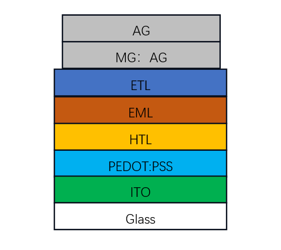
Figure 1. Diagram coupling OLED
Our investigation delves into a state-of-the-art OLED configuration, where we meticulously explore the intrinsic emission characteristics of advanced materials, as illustrated in Fig. 2. The foundation of this novel structure is a robust substrate—transparent glass—strategically precoated with a 160 nm optically conductive layer of indium tin oxide (ITO), renowned for its high transparency and electron mobility.
On top of the ITO layer, we introduce a meticulously applied 30 nm layer of poly(3,4-ethylenedioxythiophene):poly(4-styrenesulphonate) (PEDOT:PSS), a material chosen for its exceptional hole-injection and planarization properties. Progressing through the stack, a 50 nm film of N,N'-diphenyl-N,N'-bis(3-methylphenyl)-[1,1'-biphenyl]4,4'-diamine (TPD) is vacuum-deposited, serving as the hole transport layer (HTL). This is succeeded by a strategically chosen 30 nm layer of tris(8-hydroxyquinoline) aluminum (Alq3), which plays the dual role of the emissive layer (EML) and electron blocking layer due to its luminescent and electronic modulation capabilities.
For electron transport, a 50 nm layer of 2,9-dimethyl-4,7-diphenyl-1,10-phenanthroline (BCP) is utilized, enhancing the device's efficiency by optimizing electron mobility and confinement. Completing the stack is the cathode, composed of a substantial 100 nm Mg:Ag alloy with a highly conductive 60:1 Mg:Ag ratio, topped with a 20 nm thick layer of pure silver to maximize electron injection while maintaining optical transparency.
Refer to citation [24] for an in-depth exploration of our OLED device's architecture and the meticulous fabrication process. Fig. 2(b) reveals the intrinsic luminance spectrum, marked by a prominent emission peak at approximately 539 nm. By applying Equations (18)–(21) to this sophisticated layer stack, we quantify the outcoupling efficiency, normalized decay rate, and elucidate the far-field angular emission profile—each parameter being critical to the practical application of OLEDs in advanced display and lighting technologies.3.2 simulation result
|
|
|
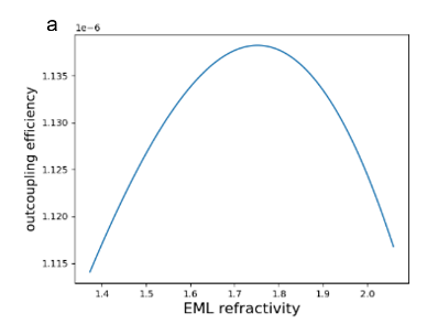
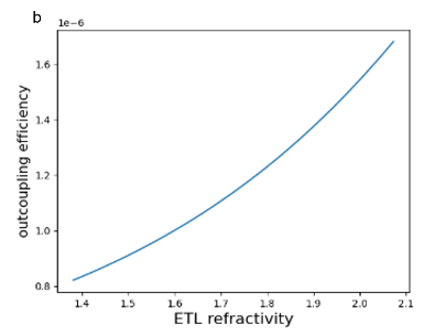
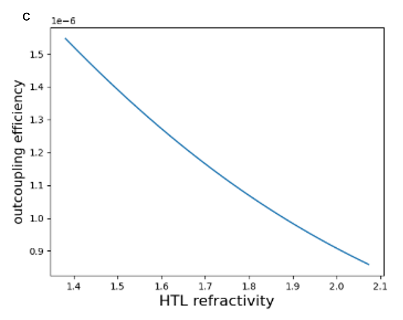
Figure 2. (a) The external coupling efficiency corresponding to different refractive indices of EML. (b) The external coupling efficiency corresponding to different refractive indices of ETL. (c) The external coupling efficiency corresponding to different refractive indices of HTL.
In our pursuit to push the boundaries of OLED technology, we conducted extensive simulations to optimize the refractive indices of the Emissive (EML), Electron Transport (ETL), and Hole Transport Layers (HTL). Our data, depicted in Figure 2a, reveals a nuanced relationship between the refractive index of the EML and the external coupling efficiency. We observed a pronounced peak in efficiency as the refractive index ascends from 1.4 to an optimal point around 1.75, beyond which the efficiency declines. A similar study on the ETL, as shown in Figure 2b, indicates a steady ascent in efficiency with a subtle plateau around the index of 1.8. Conversely, for the HTL, an increase in the refractive index from 1.4 to 2.1 corresponded with a decrease in efficiency, as illustrated in Figure 2c.
Our simulations have informed a strategic LED design that meticulously accounts for optical phenomena such as scattering, reflection, and photon trapping within the organic light-emitting layers. Discrepancies between the refractive indices of the EML and adjacent materials induce photon scattering at interfaces, which, coupled with a higher refractive index, can proliferate internal reflections. This scenario extends the photons' path within the layer, heightening the likelihood of absorption and scattering, thereby diminishing external coupling efficiency.
The ETL's role extends beyond electron transfer; its refractive index subtly modulates photon behavior at interfaces, influencing both reflection and transmission. A higher index can inadvertently enhance internal reflection, curbing the external coupling efficiency. In contrast, a lower index may facilitate photon escape, bypassing effective coupling mechanisms. Thus, we find an ETL refractive index around 1.75 to be the sweet spot that harmonizes with the EML, optimizing the light extraction process.
Designing the HTL also requires a delicate balance. The right refractive index ensures efficient photon journey towards the emission center. A mismatch in indices can skew photon paths due to refraction, scatter them, or even entrap them, all of which are detrimental to coupling efficiency. After considering these complex interactions, we conclude that a refractive index of approximately 1.75 for the HTL strikes the ideal balance, minimizing losses and promoting the outcoupling of light.
|
|
|
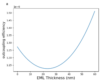
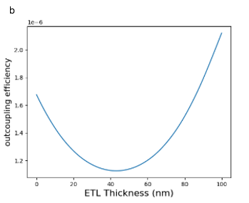
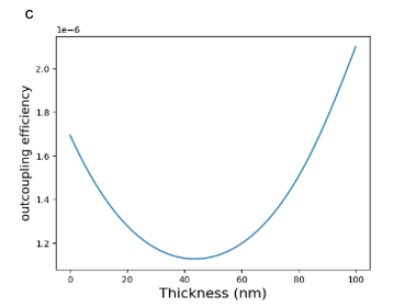
Figure 3. (a) The external coupling efficiency corresponding to different thicknesses of EML. (b) The external coupling efficiency corresponding to different thicknesses of ETL. (c) The external coupling efficiency corresponding to different thicknesses of HTL.
In our quest for optimal OLED performance, we have undertaken a comprehensive simulation to refine the thicknesses of the Emissive (EML), Electron Transport (ETL), and Hole Transport Layers (HTL). These simulations, graphically represented in Figure 3a-c, have revealed critical insights into the interplay between layer thickness and external coupling efficiency.
For the EML, our data indicates a non-linear relationship with external coupling efficiency: as the layer thickness increases from 0 to 60nm, we observe an initial decrease in efficiency, which then ascends, reaching a nadir at approximately 25nm. This suggests an optimal EML thickness range that avoids the diminishing returns of excessive thickness while maintaining sufficient material to facilitate light emission.
The trends for ETL and HTL follow a similar pattern, with optimal thicknesses presenting as a balance between too thin, which risks inadequate light reflection and potential leakage, and too thick, which could lead to excessive internal photon absorption and scattering. Our models pinpoint optimal thicknesses for both ETL and HTL at sub-20nm or in excess of 60nm, with the most efficacious thickness for ETL being upwards of 100nm, taking into account the multifaceted role of these layers in light modulation. The EML, being pivotal to the OLED structure, has its performance intricately tied to its thickness. Our findings suggest that an ideal EML thickness is around 100nm, striking a balance between having enough excited state carriers to enhance the probability of light emission and minimizing the internal scattering that can impede light outcoupling. For HTL, the thickness must be sufficient to support the transport of holes to the emission center without compromising the light's escape. We have determined from our results that a thickness exceeding 50nm is advisable to ensure a coherent propagation and outcoupling of photons, thus maximizing the efficiency of the LED device.
These findings form the bedrock of our design considerations, harmonizing the complex variables of organic material properties, device architecture, and the physics of light to engineer LEDs that stand at the forefront of efficiency and performance.
4. Conclusion
The meticulous application of the Transfer Matrix Method (TMM) in this study has paved the way for a substantial leap forward in the design and optimization of organic light-emitting diode (OLED) technologies. By navigating the complexities of wave propagation in stratified media, we have systematically dissected and enhanced the interlayer optical interactions within the OLED stack. Our simulations have yielded optimized refractive indices and precise thickness calibrations for the Emissive (EML), Electron Transport (ETL), and Hole Transport Layers (HTL), each contributing to a marked increase in external coupling efficiency.
The findings from our study underscore a critical paradigm: the optimal performance of OLEDs is achieved not by arbitrary layer construction, but through a strategic balance of material properties and geometrical configurations. The EML thickness around 100nm, ETL thicknesses under 20nm or above 60nm, and HTL thicknesses exceeding 50nm have emerged as key design parameters that dictate the proficiency of light outcoupling and overall device efficacy.
Our research presents a compelling narrative of innovation, demonstrating that the manipulation of light at the nanoscale is both an art and a precise science. The resulting knowledge serves as a beacon for future OLED design, ensuring that the next generation of devices not only meets but exceeds the rigorous demands for energy efficiency, longevity, and performance in lighting and display applications.
In conclusion, the judicious application of TMM has illuminated the path to realizing the full potential of OLEDs. This voyage of discovery has not only unraveled the intricacies of photon management within thin films but also provided a robust framework for the future landscape of optoelectronic devices.
References
[1]. Hofmann, Simone , et al. "Singlet exciton diffusion length in organic light-emitting diodes." Physical Review B Condensed Matter 85.24(2012):35-40.
[2]. Jeong, Changyeong, Yong-Bum Park, and L. Jay Guo. "Tackling light trap** in organic light-emitting diodes by complete elimination of waveguide modes." Science Advances 7.26 (2021): eabg0355.
[3]. Park, Mi **, et al. "Low absorption semi-transparent cathode for micro-cavity top-emitting organic light emitting diodes." Organic Electronics 52 (2018): 153-158.
[4]. Seo, Ji Hoon, et al. "Highly efficient white organic light-emitting diodes using two emitting materials for three primary colors (red, green, and blue)." Applied Physics Letters 90.20 (2007).
[5]. Chen, Shuming, et al. "White Organic Light‐Emitting Diodes with Evenly Separated Red, Green, and Blue Colors for Efficiency/Color‐Rendition Trade‐Off Optimization." Advanced Functional Materials 21.19 (2011): 3785-3793.
[6]. Wang, Qiang, et al. "High-efficiency organic light-emitting diodes with exciplex hosts." Journal of Materials Chemistry C 7.37 (2019): 11329-11360.
[7]. Gather, Malte C., Anne Köhnen, and Klaus Meerholz. "White organic light‐emitting diodes." Advanced Materials 23.2 (2011): 233-248.
Cite this article
Lu,H. (2024). Optically optimization of thin film light-emitting diodes based on transfer matrix. Theoretical and Natural Science,42,186-191.
Data availability
The datasets used and/or analyzed during the current study will be available from the authors upon reasonable request.
Disclaimer/Publisher's Note
The statements, opinions and data contained in all publications are solely those of the individual author(s) and contributor(s) and not of EWA Publishing and/or the editor(s). EWA Publishing and/or the editor(s) disclaim responsibility for any injury to people or property resulting from any ideas, methods, instructions or products referred to in the content.
About volume
Volume title: Proceedings of the 2nd International Conference on Mathematical Physics and Computational Simulation
© 2024 by the author(s). Licensee EWA Publishing, Oxford, UK. This article is an open access article distributed under the terms and
conditions of the Creative Commons Attribution (CC BY) license. Authors who
publish this series agree to the following terms:
1. Authors retain copyright and grant the series right of first publication with the work simultaneously licensed under a Creative Commons
Attribution License that allows others to share the work with an acknowledgment of the work's authorship and initial publication in this
series.
2. Authors are able to enter into separate, additional contractual arrangements for the non-exclusive distribution of the series's published
version of the work (e.g., post it to an institutional repository or publish it in a book), with an acknowledgment of its initial
publication in this series.
3. Authors are permitted and encouraged to post their work online (e.g., in institutional repositories or on their website) prior to and
during the submission process, as it can lead to productive exchanges, as well as earlier and greater citation of published work (See
Open access policy for details).
References
[1]. Hofmann, Simone , et al. "Singlet exciton diffusion length in organic light-emitting diodes." Physical Review B Condensed Matter 85.24(2012):35-40.
[2]. Jeong, Changyeong, Yong-Bum Park, and L. Jay Guo. "Tackling light trap** in organic light-emitting diodes by complete elimination of waveguide modes." Science Advances 7.26 (2021): eabg0355.
[3]. Park, Mi **, et al. "Low absorption semi-transparent cathode for micro-cavity top-emitting organic light emitting diodes." Organic Electronics 52 (2018): 153-158.
[4]. Seo, Ji Hoon, et al. "Highly efficient white organic light-emitting diodes using two emitting materials for three primary colors (red, green, and blue)." Applied Physics Letters 90.20 (2007).
[5]. Chen, Shuming, et al. "White Organic Light‐Emitting Diodes with Evenly Separated Red, Green, and Blue Colors for Efficiency/Color‐Rendition Trade‐Off Optimization." Advanced Functional Materials 21.19 (2011): 3785-3793.
[6]. Wang, Qiang, et al. "High-efficiency organic light-emitting diodes with exciplex hosts." Journal of Materials Chemistry C 7.37 (2019): 11329-11360.
[7]. Gather, Malte C., Anne Köhnen, and Klaus Meerholz. "White organic light‐emitting diodes." Advanced Materials 23.2 (2011): 233-248.