


1. Introduction
The impact of the near-space radiation environment on electronic devices is becoming increasingly evident with the improvement of device integration, and the resulting losses are becoming more severe [1]. Due to the many advantages of observation missions in near-space compared to satellites, reducing the impact of radiation on aircraft and spacecraft and developing corresponding protective measures have become a research focus for major aerospace powers [2, 3]. The radiation effects in near-space include: Total Ionizing Dose (TID) effects, Displacement Damage (DD) effects, and Single Event Effects (SEE) [4, 5]. These effects differ in the way they affect devices and the extent of their impact, and the corresponding protective measures also vary [4, 5],
In recent years, major aerospace powers have gained a thorough understanding of these effects and have developed relatively mature protective measures. This paper will introduce some basic concepts related to near-space radiation, review the current research on the near-space radiation environment, and summarize the protective measures against the radiation environment.
2. Related concepts
When studying radiation effects in aircraft and spacecraft, the focus is on the energy changes, i.e., the energy difference Δ𝐸, when charged particles interact with matter. To accurately describe this energy transfer, one introduces the physical concept of Linear Energy Transfer (LET), defined as \( LET=\frac{dE}{dX} \) . This formula describes the rate of change of energy as the incident particle travels through the target material. When charged particles enter the target material, they gradually slow down and, if the volume of the target material is large enough, the particles will eventually come to a complete stop. The total distance that particles travel in the target material along the direction of incidence is called the range (R). To compare the effects of different mass densities of materials on the LET and range of charged particles, the concept of mass thickness is commonly used, which is calculated by multiplying the mass density of the material with its thickness or length. LET and range are important indicators for measuring the intensity of interaction between charged particles and matter, especially LET, which plays a central role in this field.
When charged particle A interacts with target material B, it transfers energy through three main mechanisms: ionization, displacement, and bremsstrahlung radiation. For particles with small mass such as electrons, bremsstrahlung radiation also occurs. For ionization, this is the process where charged particles collide with the outer electrons of target atoms, causing the electrons to be knocked away from the atoms. The linear energy transfer of this collision is denoted as \( LE{T_{e}} \) . Displacement is the process where charged particles collide with the nuclei of target atoms, causing the nuclei to move. The linear energy transfer of this nuclear collision is denoted as \( LE{T_{n}} \) . As for bremsstrahlung radiation, when the incident particles interact with target atoms, electromagnetic radiation is produced due to accelerated motion. The linear energy transfer of this radiation is denoted as \( LE{T_{r}} \) . Considering these three mechanisms, the total linear energy transfer \( LE{T_{tot}} \) of charged particle A in target material B is composed of the sum of the three parts of energy transfer, expressed as: \( LE{T_{tot}}=LE{T_{e}}+LE{T_{n}}+LE{T_{r}} \)
When charged particles travel through an infinitely large target material, they transfer and dissipate energy through a series of collision processes, which results in a finite range. During these collision processes, not only does the speed of the incident particles gradually decrease, but their trajectories also change due to the forces they experience, a phenomenon known as scattering. It is worth noting that heavier particles typically deflect less during scattering than lighter particles.
Ionization is the primary mode of interaction between charged particles and matter. It involves inelastic collisions between incoming incident particles (with energy \( {E_{a}} \) ) and the outer electrons of the target atoms (with binding energy \( {I_{b}} \) , on the order of 10eV) through electrostatic Coulomb interaction. When \( {E_{a}} \gt {I_{b}} \) , the outer electrons of the target atom gain enough energy to break free and become free electrons with a certain energy \( {E_{fe}} \) , leaving the target atom as a positive ion, while also causing energy loss and deceleration of the incident particle. If \( {E_{fe}} \) is still greater than \( {I_{b}} \) , it can continue to cause secondary ionization. Displacement occurs when an incoming particle (with mass \( {M_{a}} \) and energy \( {E_{a}} \) ) undergoes a dynamic elastic collision with a stationary target atomic nucleus (with mass \( {M_{b}} \) ), causing the target atom to be ejected along the direction of the incident particle at an angle 𝜃 with energy:
\( {E_{b}}=\frac{4{M_{a}}{M_{b}}}{{({M_{a}}+{M_{b}})^{2}}}co{s^{2}}θ{E_{a}} \) (1)
thereby moving away from its original position and creating vacancies and interstitial atoms in the atomic lattice, introducing defects in the irradiated material. If \( {E_{b}} \) is large enough, it can continue to collide with other target atoms, causing secondary displacements.
When high-energy charged particles (with atomic number \( {Z_{a}} \) , mass number \( {A_{a}} \) , and energy \( {E_{a}} \) ) strike the spacecraft material (with atomic number \( {Z_{b}} \) ), they are decelerated by obstruction, and with the change in velocity, they radiate photons (with a continuous energy spectrum up to \( {E_{a}} \) ), which is known as bremsstrahlung radiation. The power of bremsstrahlung radiation \( ∝{({Z_{a}}{Z_{b}})^{2}}/A_{a}^{2} \) , so for actual charged particles, electrons, due to having the same charge number as protons but a mass of only about \( 1/1837 \) of that of protons, have a bremsstrahlung radiation power that is \( {10^{6}} \) times that of protons under the same conditions, which is particularly prominent. Therefore, for space radiation particles mainly composed of electrons, protons, and heavy ions, the bremsstrahlung radiation effect of electrons is primarily considered [3]. In the space radiation environment, when electrons pass through materials such as satellite skins and electronic device casings, they are decelerated by obstruction, producing X-rays. These secondary X-rays have strong penetrating power and continue to penetrate electronic device casings or device encapsulations, producing ionizing radiation doses at critical devices, leading to Total Ionizing Dose effects [2, 3].
3. Types of radiation damage in near-space
The types of radiation in near-space are mainly divided into three types, i.e., Total Ionizing Dose (TID) effects, Displacement Damage (DD) effects, and Single Event Effects (SEE) [2, 3]. The Total Ionizing Dose effect (also known as TID effect) is the impact caused by the ionizing action of space radiation particles, which is positively correlated with the cumulative dose. These radiations produce additional electron-hole pairs through the ionization process in the material of the device, which move, evolve, and are captured within the device, ultimately affecting the performance of the device. For spacecraft, the TID effect on the operational devices is the most prominent, with the cumulative ionizing charge causing the device's operating parameters to gradually degrade and eventually fail. On April 5, 2010, the "Galaxy 15" satellite of the World Teleport Communication Organization suffered a failure. Through verification, this failure was caused by deep charge discharge leading to device damage and satellite failure [1].
As shown in the Fig. 1, the Displacement Damage effect is caused by the elastic collision between space radiation particle A and the atom B of the target material, causing the target material atom to move as shown in the figure below, including the target atom leaving its original position to become an interstitial atom and leaving a vacancy at the original position of the target atom. The degree of displacement of the target material atom is related to the elastic collision energy received by the target material per unit mass of radiation particles, denoted as Displacement Damage Dose (DDD), which is also called Displacement Damage effect. This effect can be caused by the bombardment of a single particle.
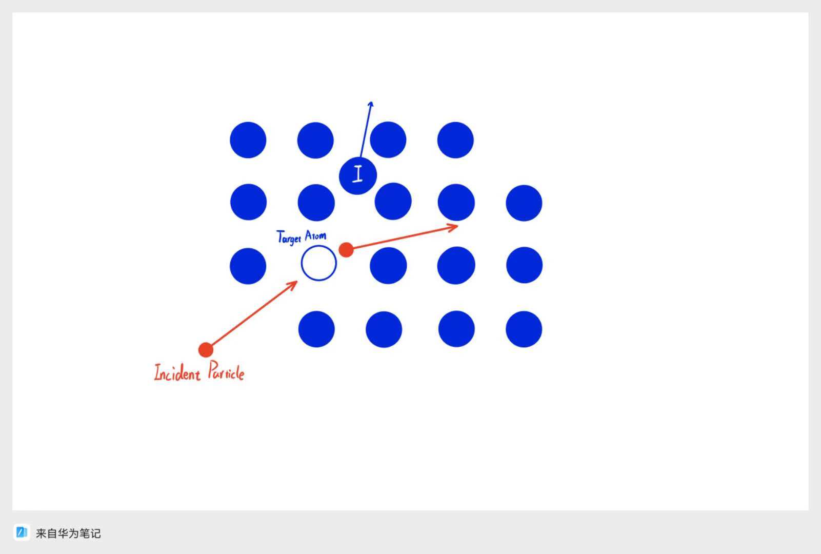
Figure 1. Displacement Damage Effects (Photo/Picture credit: Original).
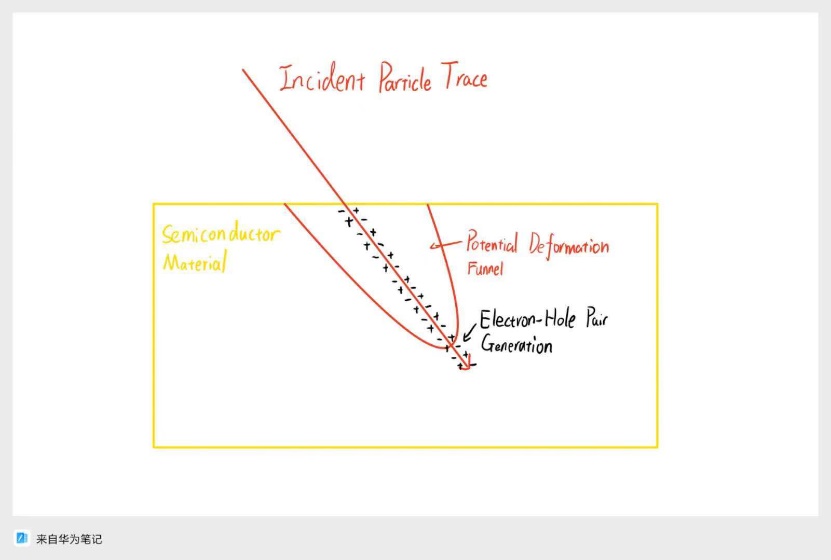
Figure 2. Single Event Effects (Photo/Picture credit: Original).
There are various types of Single Event Effects, and their most fundamental process involves three stages. A single charged particle travels through the device material, forming an instantaneous ionization action that creates an electron-hole pair column along its trajectory. The sensitive nodes in the device collect the ionizing charge to form a transient current pulse. The transient current pulse impacts the specific functional parts of the device circuit, inducing various types of Single Event Effects. A sketch is shown in Fig. 2. The main Single Event Effects include:
• Single-Event Upset (SEU). A logic error in the circuit caused by a potential error due to a single particle strike.
• Single-Event Latch-up (SEL). When a high-energy particle strikes a CMOS device, it may trigger a state known as latch-up, where some parts of the device consume abnormally high current, causing device damage or performance degradation.
• Single Event Transient (SET). In logic circuits, a single particle strike may cause a brief change in current or voltage, and this transient effect may affect the normal operation of the circuit.
• Single Event Functional Interrupt (SEFI). A high-energy particle strike may temporarily interrupt some functions of the system or device.
• Single Event Burnout (SEB). Due to a large current caused by a single particle, in power MOSFETs and other devices, a single high-energy particle may cause permanent damage to the device.
• Single Event Gate Rupture (SEGR). Similar to SEB, it is a device failure caused by a large current. This effect causes gate damage.
Among them, SEL, SEB, and SEGR are destructive Single Event Effects, which are highly destructive once damage occurs and are currently difficult to remotely repair. SEU, SET, and SEFI are non-destructive Single Event Effects, which can generally be restored to some extent through various software and hardware means. A more serious loss occurred in 2011, when the "Phobos-Grunt" Mars probe launched by Russia, after reaching low orbit and only about 3 hours after launch, suffered a single particle strike on a key device causing a Single-Event Latch-up, preventing the execution of the expected ignition command, and ultimately the satellite fell into the Earth's atmosphere [6].
4. Total Ionizing Dose (TID) Effect Protection Design
In specific circuit design, tolerance design can be used to ensure that the circuit system can operate normally within a wider range of electrical parameters, or even when there is a certain degree of deviation. However, in general, when conducting TID irradiation experiments, tolerance has often been considered already, so there is not much room for tolerance design. Redundant backup is a frequent practice to improve system reliability. For redundancy design actively carried out due to TID reasons, or redundancy design that improves the TID level by taking advantage of basic reliability backups, it is necessary to determine through experiments and research which redundancy mode (cold backup, hot backup, warm backup, etc.) has the least TID impact or is safe. Based on the overall design of the spacecraft, the impact of TID effects can be reduced, for example, by arranging more critical devices in the center of the spacecraft.
Individual equipment can assess the radiation dose through a simple method. First, consider the thickness of the equipment case and the thickness of the satellite shell (usually 0.8 mm aluminum material), and then use the dose-thickness relationship curve obtained from experimental data to estimate the radiation dose that the equipment may withstand. Through this assessment, it can be determined whether the TID tolerance of the electronic devices used meets the required standards. If the assessment results show that the tolerance of the devices is insufficient, the thickness of the case can be increased within the weight limit of the equipment, or shielding materials can be locally added to key electronic devices to improve their radiation resistance and meet the requirements for radiation protection. For key devices, the shielding contribution of the internal PCB board of the case can also be further considered, as shown in the Fig. 3. For the device shown in the figure above, in addition to the shielding of the case thickness \( {d_{case}} \) on all six sides, considering that the area of the internal PCB board is large and the shielding blockage solid angle for key devices is large, ignoring the lack of shielding in the direction parallel to the PCB board, it is artificially assumed that the one-dimensional shielding thickness received by the key device from the case and the PCB board ( \( {d_{i}} \) ) is \( {d_{case}}+\frac{1}{2}({d_{1}}+{d_{2}}+{d_{3}}+…+{d_{n}}) \) . The radiation dose under this shielding thickness can be evaluated according to the dose-thickness curve to see if it meets the requirements.
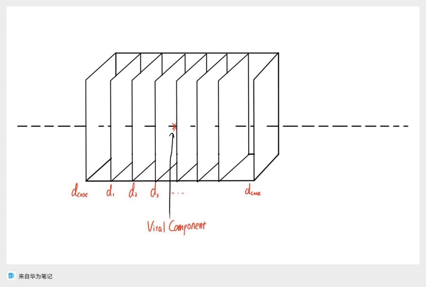
Figure 3. The One-Dimensional Shielding Design (Photo/Picture credit: Original).
The above solid sphere one-dimensional shielding design can quickly give a safe shielding design for satellites without mass cost burden, mainly considering the shielding of the satellite shell and the individual equipment case that the spacecraft internal single machine designer is concerned about, and ignoring the shielding effect of other instruments, parts, structures, etc., inside the spacecraft on the single machine equipment of interest, which is a conservative design. For satellites with high TID index and limited mass resources (such as MEO satellites), it is necessary to comprehensively analyze the shielding effects of those details ignored by the one-dimensional model, and carry out additional shielding design on this basis. Therefore, it is necessary to perform three-dimensional shielding analysis and design for satellites with complex material composition and structural layout. For the calculation of radiation dose, two sets of experimental data are generally required: the shielding thickness statistical distribution data F( \( {d_{i}} \) ) and the one-dimensional dose-thickness curve data D( \( {d_{i}} \) ) of the spacecraft mission. The unit of thickness uses equivalent thickness of aluminum. The following are examples of the two sets of curves in Fig. 4 [7]. Using the following formula, the more realistic radiation dose after the complex spacecraft structure layout can be calculated.
\( Dose=\frac{1}{4π}\sum _{1}^{n}D({d_{i}})·F({d_{i}}) \) (2)
For the model of the spacecraft, modeling software such as ProE or COSMIC can be used for modeling, and the protection plan can be analyzed and specifically designed for the dose.
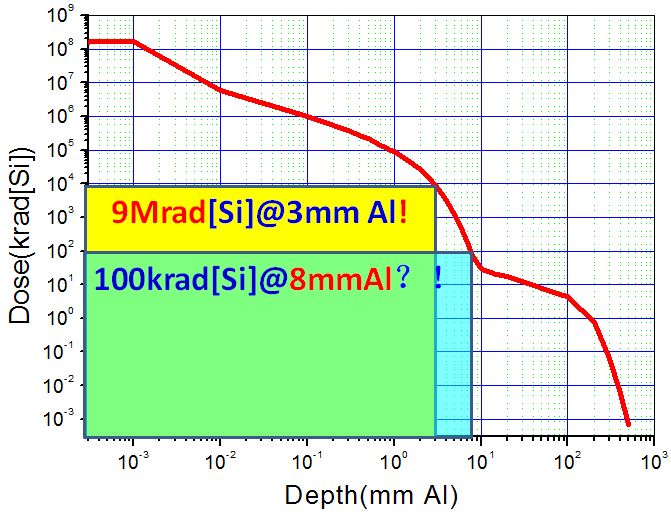
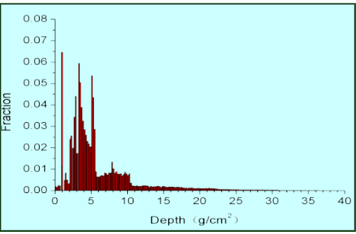
Figure 4. One-dimensional dose-depth curve D( \( {d_{i}} \) ) of a certain MEO satellite (left) and shielding thickness statistical distribution chart F( \( {d_{i}} \) ) [7].
In the aforementioned chapters, for the transmission and shielding calculation of space charged particles in the spacecraft material, the spacecraft material is simplified to aluminum material, and the common electronic equipment case also uses aluminum alloy. For the local shielding of key devices, in order to save space, materials with larger mass density and atomic number, such as lead or tantalum, are used. High-density materials can better absorb high-energy photons (such as X-rays) compared to low-density materials. Therefore, after the low-density material decelerates the electrons, the high-density material can absorb the bremsstrahlung radiation (X-rays) caused by the deceleration of electrons to reduce radiation damage. For materials with a medium thickness (about 3-10mm), composite materials made of aluminum and tantalum in a certain ratio (20%-30% aluminum content of tantalum-aluminum composite material) can better shield radiation. For the protection of key devices, considering the space saving and the good protection performance of pure tantalum under a thinner thickness (less than 3mm), pure tantalum is generally used for protection. For large thickness parts, due to the payload requirements of aerospace, pure aluminum is generally used [3, 8].
A research result in August 2018 mentioned the current protection measures for TID effects [4]. According to the calculation results of the radiation protection software, for a specific optical system structure model, a protective cover can be added in front of the lens to enhance protection. This protective cover design is simple and can be flat or concave, and should have the same engineering installation characteristics as the light-blocking cylinder components in front of the lens in the model. Following the principle of minimizing the mass of the satellite, it is recommended that the thickness of the protective cover be between 1 and 3 millimeters, and to achieve the best protective effect, the protective cover should be located no more than 20 millimeters in front of the lens [4]. The quantitative data calculated by the software shows that after the shielding of the protective cover with a thickness of 1 to 3 millimeters, the contribution of the radiation dose to the most severe environmental parts through the exposed window of the Earth's radiation belt can be reduced to one to ten percent of the original radiation dose, that is, the radiation dose is reduced by two orders of magnitude [4]. If the on and off time ratio of the remote sensor in orbit has been further considered, the radiation dose at the main mirror can be further reduced. For extremely high-energy galactic cosmic ray particles, the dose change before and after protection is not significant. However, due to the very small dose contribution of such particles, they are usually negligible. Considering the analysis above, the protection scheme using a protective cover can significantly reduce the radiation absorption dose of the remote sensor in the most severe environment, bringing the radiation absorption dose of this part to the same order of magnitude as other parts of the optical system, thereby effectively enhancing the radiation protection performance of the system [4].
5. Displacement damage protection design
The Displacement Damage effect is similar to the Total Ionizing Dose effect, both being caused by the cumulative effect of low to medium energy but high flux radiation belt particles and solar protons leading to the degradation of electrical parameters. Therefore, the protective design concepts for the Total Ionizing Dose effect are also applicable to the protection design for Displacement Damage effects. However, when designing proton shielding, it is necessary to consider that the lower the proton energy, the greater the displacement damage effect it causes. Therefore, a careful analysis and calculation of the impact of lower energy protons after material shielding is required.
6. Single event effect protection design
The types of Single Event Effects (SEEs) that occur in devices and the impacts they have on circuits and equipment vary, and so do the corresponding protective design strategies and methods. The following table is a ranking of the Single Event Effects that space missions need to focus on, considering both the frequency of occurrence in orbit and the resulting hazards. The ranking is in order of concern, starting with CMOS device Single Event Latch-up (SEL), digital device Single Event Functional Interrupt (SEFI) and Single Event Upset (SEU), power device Single Event Burnout (SEB), and analog device Single Event Transient (SET) (seen from Table 1). The guiding principle of Single Event Effect (SEE) protection design is risk management. The following are the protective design approaches and main methods for destructive and non-destructive Single Event Effects, respectively. It is necessary to avoid and reduce the probability of destructive Single Event Effects (SEEs); uses devices with a high Linear Energy Transfer (LET) threshold; derate the operating voltage of power devices (operate at less than 50% of the safe working voltage for Single Event Burnout (SEB) and Single Event Gate Rupture (SEGR)). SEL current limiting and recovery: Utilize smart circuits that autonomously detect and determine the occurrence of Single Event Latch-up (SEL), actively cut power, wait for an appropriate duration, and then reapply power; or through ground personnel, manually determine the occurrence of SEL, and manually send commands to cut and reapply power; also consider periodic automatic power cycling to eliminate potential latch-ups [9]. One also needs to implement backup designs for critical components and circuits. Besides, it is necessary to detect and mitigate the effects of non-destructive Single Event Effects (SEEs). For SEU-induced data errors, redundancy voting in hardware and software, Error-Detecting and Correcting (EDAC) codes, refreshing, reconfiguration. SEFI-induced system malfunction (detection and recovery); error counters, watchdog timers; built-in or external health diagnostic management units. Partial or full refreshing of components; system reset, power cycling SET (Single Event Transient); logic units: temporal redundancy; power circuits: Filtering, voltage regulation; restart to address potential latch-ups; linear or interface circuits: filtering, and possible SEU protection in subsequent connected digital circuits.
Table 1. Single Event Effects of Concern for Spacecraft Missions
Priority | Single Event Type | Severity (from 1 to 5) | Frequency (from 1 to 5) | Note |
1 | CMOS SEL | Severe 4 | Frequent 4 | Hard to suppress its occurrence; it can only be recovered by power cycling. |
2 | SEFI, SET | Medium 2 | Very Frequent 5 | Error correction and recovery can be performed. |
3 | SEB | Very Severe 5 | Seldom 1 | A hard error that cannot be fixed, limiting current is the only option. |
4 | SET | Light 1 | Very Frequent 5 | In a few cases, the fluctuations can pose significant hazards. |
In 2021, a research team mentioned that they conducted a series of laser pulse irradiation experiments on the CMOS process SRAM model CY62167DV30LL, with the aim of exploring its Single Event Latch-up (SEL) characteristics, and quantitatively calculated the holding voltage and holding current of the SRAM in the latched state through these experiments [10]. Based on these electrical characteristics and latching conditions, the team proposed two circuit-level protection methods: voltage division resistors and power supply current limiting. Both methods are easy to implement and do not affect the normal function of the device, and have high engineering practicality. For this SRAM, the range of holding voltage \( {V_{hold}} \) is 1.5 to 1.6 volts, and the range of holding current \( {I_{hold}} \) is 9.9 to 11.2 milliamperes. For this chip, the power supply current limiting method successfully brought the device out of the Single Event Latch-up state. To achieve this, the limiting current value should be greater than the device's standard operating current of 2 milliamperes and less than the holding current of 10.3 milliamperes. Similarly, by using the method of connecting a voltage division resistor in the circuit, the device was also successfully brought out of the Single Event Latch-up state. Under standard working conditions, the minimum value of the resistor should be between 60 and 70 ohms, and the maximum value should not exceed 500 ohms. Although this circuit-level protection strategy cannot completely prevent the occurrence of Single Event Effects (SEEs) and SRAM data errors caused by large current surges, it can quickly bring the device out of the latched state. On the one hand, this can prevent the device from being damaged due to continuous operation in a high current state; on the other hand, it can significantly reduce the number of data anomalies and limit errors to a smaller area centered on sensitive points. Therefore, by using an interleaved storage of data, combined with traditional error detection and correction methods, the correctness of the data can be ensured [10].
7. Limitations and prospects
All current protective measures aim to mitigate radiation damage, and it is not possible to completely eliminate damage within the payload allowance at a low cost. Possible future research directions include following. For biomembrane, melanin produced by some fungi can absorb radiation very well or convert high-energy photons into low-energy photons. This may help reduce the impact of Total Ionizing Dose (TID) effects. For quantum mechanical principle devices, the devices that do not rely on electrons as charge carriers and information transmission particles (such as the polarized photons used in quantum encryption) may help reduce the impact of electron-hole pairs generated by high-energy particles on the device.
8. Conclusion
To sum up, this study introduces the types of radiation damage in the near-space radiation environment and corresponding protective measures. The types of radiation damage include Total Ionizing Dose (TID) effects, Displacement Damage (DD) effects, and Single Event Effects (SEE), with damage sources from ionization, displacement, and bremsstrahlung radiation. The protection strategy for TID involves calculating the shielding effect contributed by the materials of the spacecraft to determine the absorbed dose of the devices. For the protection against Displacement Damage, the strategy is similar, focusing on material shielding to mitigate the effects. The guiding principle for the protection strategy against SEE is risk management, aiming to minimize the probability of catastrophic SEE and to detect and mitigate the impact of non-destructive SEE. Current strategies for future radiation protection may involve the use of biomembranes to absorb radiation or the application of quantum mechanics principles to eliminate the effects brought about by radiation.
References
[1]. Progress has been made in the experimental study of the failure of the YH-15 communication satellite at the Space Center. Progress made in the experimental study on the failure of the YH-15 communication satellite at the Space Center, CAS 2010 Retrieved from: https://www.cas.cn/ky/kyjz/201005/t20100513_2844669.shtml
[2]. Wang N, Ma L L, Liu Q, et al. 2023 The near-space altitude experiment for satellite radiometric calibration and the first results. National Remote Sensing Bulletin 27(5) 1177-1193.
[3]. Zhang Y 2018 Research of X-ray/Electrons Induced Single Event Soft Errors in 45nm SRAM. Xiangtan University.
[4]. Zhang X, Zhao X and Li X 2018 Protection method for total dose effect on the optical system of typical satellite remote sensor and related design. Key Laboratory for Optical Remote Sensor Technology of CAST, Beijing Institute of Space Mechanics & Electricity 11.
[5]. Wang C 1997 The Influence with Reliability of Motional Satellite by the Single-Event Phenomena. Shijiazhuang. China Electronics Technology Group Corporation thirteenth Research Institute.
[6]. Han J, Feng G, Yu Y et al. 2014 Analysis of Single-event Effects Rate of K6R4016V1D Chips Applied in Low Earth Orbit. Chinese Journal of Space Science 35(1) 64-68.
[7]. Zou S, Xue B, Liu Z, Zhou X and Sheng L 2017 Design of shielding for GEO satellite and analysis for its effectiveness. Spacecraft Environmental Engineering 4 410-414.
[8]. Hu Z, Li Z, Zhang T and Zhang X 2003 New Development and Applications of Tantalum and Tantalum Alloys. Rare metals and hard alloys 3 34-36+48
[9]. Wu H, Zhu X, Han J 2021 Research on Circuit Level Protection Design of SRAM Single Event Latch-up Effect. Atomic Energy Science and Technology 4 758-766.
[10]. Hu X, Wei F, Li L et al. 2022 In-situ environmental detecting payloads onboard the floating platform in near-space. Aerospace Technology 3 95-104.
Cite this article
Qi,X. (2024). Near-space radiation environment analysis and protective measures. Theoretical and Natural Science,52,1-9.
Data availability
The datasets used and/or analyzed during the current study will be available from the authors upon reasonable request.
Disclaimer/Publisher's Note
The statements, opinions and data contained in all publications are solely those of the individual author(s) and contributor(s) and not of EWA Publishing and/or the editor(s). EWA Publishing and/or the editor(s) disclaim responsibility for any injury to people or property resulting from any ideas, methods, instructions or products referred to in the content.
About volume
Volume title: Proceedings of CONF-MPCS 2024 Workshop: Quantum Machine Learning: Bridging Quantum Physics and Computational Simulations
© 2024 by the author(s). Licensee EWA Publishing, Oxford, UK. This article is an open access article distributed under the terms and
conditions of the Creative Commons Attribution (CC BY) license. Authors who
publish this series agree to the following terms:
1. Authors retain copyright and grant the series right of first publication with the work simultaneously licensed under a Creative Commons
Attribution License that allows others to share the work with an acknowledgment of the work's authorship and initial publication in this
series.
2. Authors are able to enter into separate, additional contractual arrangements for the non-exclusive distribution of the series's published
version of the work (e.g., post it to an institutional repository or publish it in a book), with an acknowledgment of its initial
publication in this series.
3. Authors are permitted and encouraged to post their work online (e.g., in institutional repositories or on their website) prior to and
during the submission process, as it can lead to productive exchanges, as well as earlier and greater citation of published work (See
Open access policy for details).
References
[1]. Progress has been made in the experimental study of the failure of the YH-15 communication satellite at the Space Center. Progress made in the experimental study on the failure of the YH-15 communication satellite at the Space Center, CAS 2010 Retrieved from: https://www.cas.cn/ky/kyjz/201005/t20100513_2844669.shtml
[2]. Wang N, Ma L L, Liu Q, et al. 2023 The near-space altitude experiment for satellite radiometric calibration and the first results. National Remote Sensing Bulletin 27(5) 1177-1193.
[3]. Zhang Y 2018 Research of X-ray/Electrons Induced Single Event Soft Errors in 45nm SRAM. Xiangtan University.
[4]. Zhang X, Zhao X and Li X 2018 Protection method for total dose effect on the optical system of typical satellite remote sensor and related design. Key Laboratory for Optical Remote Sensor Technology of CAST, Beijing Institute of Space Mechanics & Electricity 11.
[5]. Wang C 1997 The Influence with Reliability of Motional Satellite by the Single-Event Phenomena. Shijiazhuang. China Electronics Technology Group Corporation thirteenth Research Institute.
[6]. Han J, Feng G, Yu Y et al. 2014 Analysis of Single-event Effects Rate of K6R4016V1D Chips Applied in Low Earth Orbit. Chinese Journal of Space Science 35(1) 64-68.
[7]. Zou S, Xue B, Liu Z, Zhou X and Sheng L 2017 Design of shielding for GEO satellite and analysis for its effectiveness. Spacecraft Environmental Engineering 4 410-414.
[8]. Hu Z, Li Z, Zhang T and Zhang X 2003 New Development and Applications of Tantalum and Tantalum Alloys. Rare metals and hard alloys 3 34-36+48
[9]. Wu H, Zhu X, Han J 2021 Research on Circuit Level Protection Design of SRAM Single Event Latch-up Effect. Atomic Energy Science and Technology 4 758-766.
[10]. Hu X, Wei F, Li L et al. 2022 In-situ environmental detecting payloads onboard the floating platform in near-space. Aerospace Technology 3 95-104.