


1. Introduction
In modern electronics, the demand for higher frequency and higher power devices is driven by the need for more efficient power conversion, faster data processing, and enhanced performance in applications ranging from telecommunications to advanced computing systems. To meet these requirements, GaN HEMTs are becoming increasingly important due to their superior material properties compared to traditional Silicon based devices. As a wide bandgap semiconductor (Eg = 3.4 eV), GaN allows for higher breakdown voltages (4MV/cm) [1] and better performance in high-voltage environments, which is crucial for power electronics and RF devices where high voltage and power levels are necessary [2]. Furthermore, GaN HEMTs possess high electron mobility, resulting in faster switching speeds and higher frequencies of operation, which is particularly advantageous for RF and microwave applications [3]. They also exhibit better thermal stability and heat dissipation compared to Si devices, allowing for reliable performance under high-temperature conditions [4]. The robustness of GaN HEMTs makes them suitable for use in harsh environments such as space and military applications, as they can withstand radiation and high temperatures without significant performance degradation [5].
T-shape gate structure has been introduced to GaN HEMT to enhance the device's frequency performance. This is because T-shape gate can enhance the controllability to the channel without increasing the contact resistance [6]. M. Cho et al. developed a T-gate process for AlGaN/GaN-based fin-type HEMTs, achieving improved radio-frequency (RF) performance with a cut-off frequency of 9.7 GHz and a maximum oscillation frequency of 27.8 GHz, indicating a significant enhancement in RF capabilities due to the T-gate design [7]. Yeke Liu et al. demonstrated T-gate high-frequency AlGaN/GaN HEMTs on an extremely low resistivity silicon substrate, achieving cut-off frequency of 27 GHz, maximum oscillation frequency of 71 GHz, and a maximum transconductance of 247 mS/mm [8]. Jielong Liu et al. introduced millimeter-wave AlGaN/GaN MIS-HEMTs with Multiple T-gate technology, demonstrating superior frequency characteristics due to improved 2DEG mobility, which resulted in cut-off frequencies (ft) of 87 GHz and maximum oscillation frequencies (fmax) of 158 GHz, showing the potential of T-gate structures on silicon substrates for RF application [9].
2. Device architecture
The structure of the device is illustrated in Figure 1. SiC is utilized as the substrate due to its high thermal conductivity. AlN layer serves as the nucleation layer to further reduce the lattice mismatch between the substrate and the GaN buffer layer. The Al content in the aluminum AlGaN barrier layer is 30%, which enhances both the piezoelectric polarization effect and the spontaneous polarization effect of the device. The GaN cap layer primarily acts as the surface layer of the device. By introducing surface donors to this layer, the two-dimensional electron gas (2DEG) beneath it can be modulated. The layer is doped to a concentration of 1E16/cm³ in the paper to enhance conductivity, which facilitates the formation of ohmic contacts.
Table 1 and Table 2 shows the device dimension and parameter used in simulation.
Table 1: Device dimension of T-gate GaN HEMT
Layer | Thickness | Length |
Si3N4 passivation layer thickness | 0.05μm | -- |
GaN cap layer | 2nm | 200nm |
AlGaN barrier layer | 11nm | 200nm |
GaN buffer layer | 1.8μm | 400nm |
AlN nucleation layer | 120nm | 400nm |
Source contact | 67nm | 100nm |
Drain contact | 67nm | 100nm |
T-gate head | 5nm | 120nm |
T-gate foot | 100nm | 100nm |
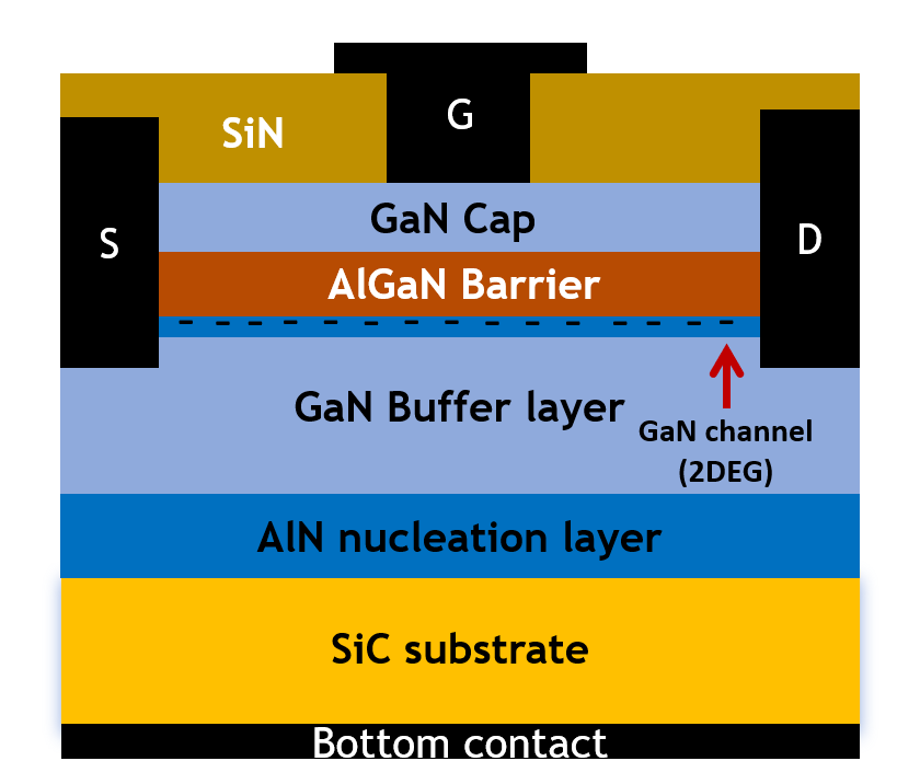
Figure 1: Schematic figure of T-gate GaN HEMTs for TCAD simulation
Table 2: Some important parameters of GaN and AlGaN used in simulation
Parameter | GaN | AlGaN |
Eg@300K (eV) | 3.4 | 3.9 |
Permittivity | 9.4 | 9.4 |
Nc@300K (cm-3) | 1E18 | 2E18 |
NV@300K (cm-3) | 1.18E18 | 1.18E18 |
3. Simulation approach
The device structure is defined and edited in the SDE. Specifically, the 5 nm GaN channel is designated as a separate region to facilitate subsequent modifications to model parameters. For the simulation of the device's electrical performance, the accurate selection of physical models is crucial for obtaining precise results. We selected the Doping Dependence Model and High Field Saturation Model for mobility. This choice is because wide-bandgap materials typically operate under high voltages, causing electrons to reach saturation velocity, deviating from the low-field rule (𝑣=𝜇⋅𝐸). The High Field Saturation Model accurately represents device behavior under these conditions. For the recombination model, we activated the SRH model and radiative model because the carrier concentration in the GaN HEMTs channel is very high, making recombination very important. The radiative model can effectively characterize the recombination in the quantum well, while the SRH can well represent the recombination phenomenon under high electron concentration. For the polarization phenomenon of GaN material, we activated a simple strain-based piezoelectric polarization model. We also activated the thermionic current model for electrons at a region-interface for heterojunction.
4. Results and discussion
Figure 2 (a) shows the output characteristics (ID-VD) curve of the T-gate GaN HEMT. As the applied gate voltage increases the maximum drain current increases. When 𝑉𝐺=2𝑉and 𝑉𝐷=2.4𝑉, the maximum drain current of the GaN HEMT can reach 1300 mA/mm. Figure 2 (b) shows the variation trend of the leakage current with changes in gate voltage. We can observe that when 𝑉𝐷=5𝑉 and 𝑉𝐺<1𝑉, the drain current remains at a relatively low level.
Figure 2 (c) shows the transfer characteristics of (ID-VG) curve of the T-gate GaN HEMT at VD=5V. The device's threshold voltage Vth is -2.07V. The transconductance (𝑔𝑚) reaches its maximum value of 511.4 mS/mm. And from Equation 1, we can see that the cutoff frequency increases with the transconductance. As shown in Figure 2 (d), the cutoff frequency exhibits a trend similar to that of the gm-𝑉G changes, reaching a peak value of 138 GHz at 𝑉𝐺=−0.65V.
\( {f_{t}}=\frac{{g_{m}}}{2π{C_{gg}}} \) (1)
The relationship between 𝑓𝑚𝑎𝑥 and 𝑉𝐺 is shown in Figure 2 (e). In the region of higher gate voltage, since the device is already fully turned on, further increasing the gate voltage actually reduces 𝑓𝑚𝑎𝑥.
To further understand the impact of device structure on its RF performance, we next simulated devices with different parameters.
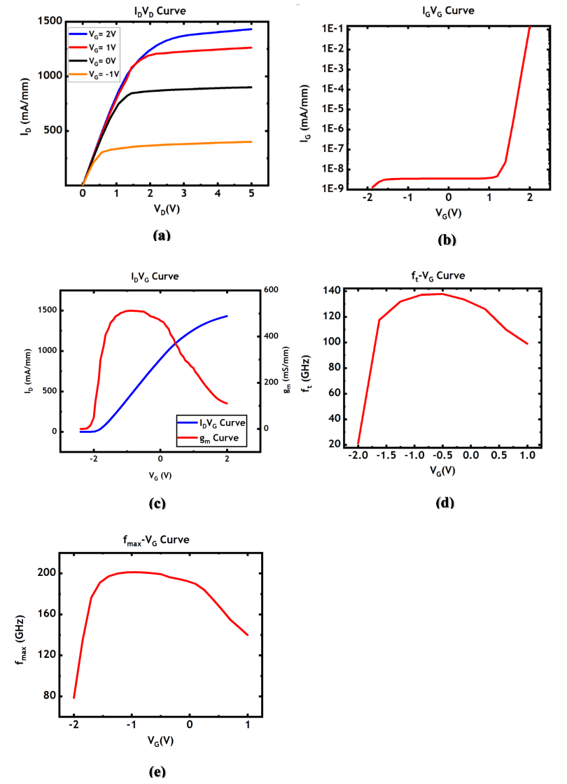
Figure 2: The (a) ID-VD curve; (b) IG-VG curve; (c) IDVG curve; (d) ft-VG curve and (e) fmax-VG curve of T-gate GaN HEMT
The gate length typically affects the RF performance of the device. As shown in Figure 3 (a), an increase in gate length results in a decrease in transconductance. According to Equation 1, this leads to a corresponding decrease in cut-off frequency. Additionally, the increased gate length also raises the gate leakage current, which also reduces 𝑓𝑚𝑎𝑥 of device.
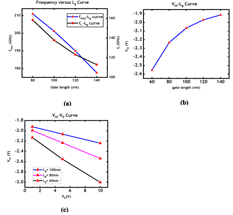
Figure 3: (a) maximum oscillation frequency amd cut-off frequency; (b) threshold voltage; (c) drain-induced barrier lowering effect of device with different gate length
However, shortening the gate length can cause short-channel effects. As shown in Figure 3 (b) and Figure 3 (c), when the gate length is less than 100 nm, noticeable 𝑉𝑡ℎ roll-off and drain-induced barrier lowering (DIBL) phenomena occur.
Traps are widely distributed throughout the device, primarily due to material defects, dopant atoms, lattice mismatch, and dangling bonds on the crystal surface. Additionally, deep-level traps (such as Fe doping) are intentionally introduced into the device to adjust the cutoff frequency and maximum oscillation frequency. These traps, due to electron capture effect, significantly affect the device's performance at high frequencies. Traps introduce in the paper is shown in Table 3.
Since the device's response to AC signals is based on electron migration between the GaN and AlGaN layers, AlGaN/ GaN interface traps can affect the high-frequency performance by influencing this migration. The impact of traps on electron capture can be seen in Figure 4 (a). When the trap concentration increases, the captured electron concentration also increases, resulting in a corresponding increase in the threshold voltage. Similarly, traps can also capture electrons leaking from the gate contact, thereby reducing gate leakage current, as shown in Figure 4 (b).
Table 3: The properties of two different types of traps in the device
Location of traps | AlGaN/GaN interface | GaN buffer layer |
Distribution | Gaussian distribution | Uniform |
Concentration | CGTrap cm−2 (at peak) | Ntp cm−3 |
Type | Acceptor - like | Acceptor - like |
Capture area | 1E14 cm2 | 1E14 cm2 |
As illustrated in Figure 4 (c), an increase in trap concentration at the AlGaN/ GaN interface due to the capture effect makes it difficult for electrons to migrate from the AlGaN surface to the GaN layer in response to changing signals. This leads to a degradation in high frequency performance, including the cut-off frequency and maximum oscillation frequency. However, in the region of low trap concentration, the traps at the interface can also reduce gate leakage current, which results in a gradual increase in the maximum oscillation frequency.
Because GaN HEMTs use a 2DEG as their conductive channel, the electron concentration of the 2DEG is key to achieving high electron mobility. To enhance the spatial confinement of the 2DEG, an effective method is to introduce deep-level traps in the GaN buffer layer. The trend of the device's high-frequency performance with varying trap concentration in the GaN buffer layer is shown in Figure 4 (d). It can be seen that as the trap concentration increases, the 2DEG is confined to a very thin layer, increasing the electron concentration in the channel. This, in turn, improves the device's cut-off frequency and maximum oscillation frequency.
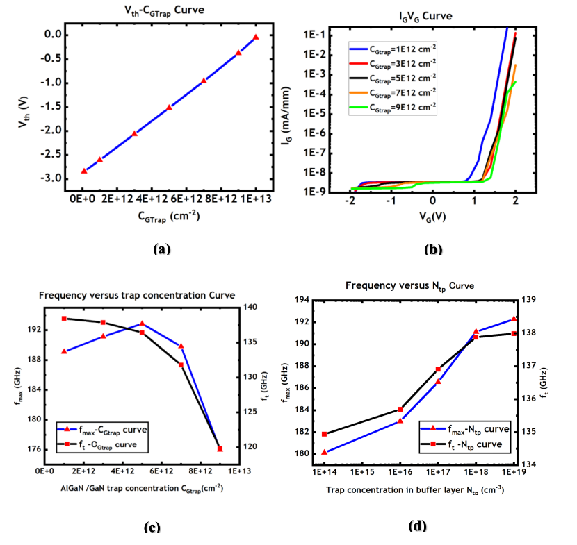
Figure 4: The (a) threshoald voltage; (b)IG-VG curve; (c) cut-off frequency and maximum oscillation frequency as a function of interface traps concentration and (d) cut-off frequency and maximum oscillation frequency as a function of traps concentration in GaN buffer layer
5. Conclusion
In this paper, DC and AC characteristics have been investigated for T-gate GaN HEMTs. The device exhibits a maximum drain current exceeding 1300 mA/mm, with a peak transconductance of 511.4 mS/mm and a gate leakage current below 1E-8 mA/mm. We also compare the frequency performance of our device with other papers, as shown in Figure 5, [8,10-13] and it can be seen that the GaN HEMTs in the paper have both high cutoff frequencies and high maximum oscillation frequencies.
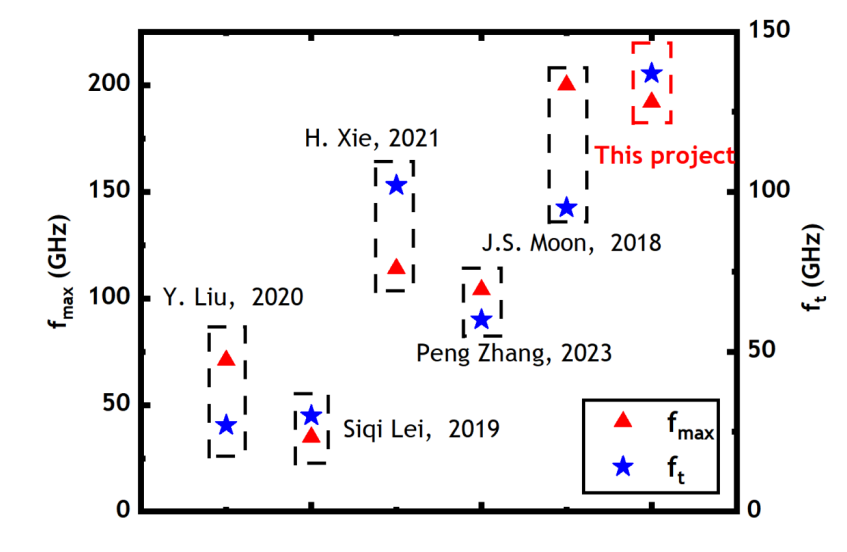
Figure 5: Comparation of GaN HEMTs frequency performance between our project and other paper
References
[1]. M. S. Adler, K. W. Owyang, B. J. Baliga, and R. A. Kokosa, ‘The evolution of power device technology’, IEEE Trans. Electron Devices, vol. 31, no. 11, pp. 1570–1591, Nov. 1984, doi: 10.1109/T-ED.1984.21754.
[2]. U. K. Mishra, L. Shen, T. E. Kazior, and Y.-F. Wu, ‘GaN-Based RF Power Devices and Amplifiers’, Proc. IEEE, vol. 96, no. 2, pp. 287–305, Feb. 2008, doi: 10.1109/JPROC.2007.911060.
[3]. W. Johnson and E. L. Piner, ‘GaN HEMT Technology’, in GaN and ZnO-based Materials and Devices, S. Pearton, Ed., Berlin, Heidelberg: Springer, 2012, pp. 209–237. doi: 10.1007/978-3-642-23521-4_7.
[4]. X. Cai et al., ‘Recent progress of physical failure analysis of GaN HEMTs’, J. Semicond., vol. 42, no. 5, p. 051801, May 2021, doi: 10.1088/1674-4926/42/5/051801.
[5]. T. Satoh, K. Osawa, and A. Nitta, ‘GaN HEMT for Space Applications’, in 2018 IEEE BiCMOS and Compound Semiconductor Integrated Circuits and Technology Symposium (BCICTS), Oct. 2018, pp. 136–139. doi: 10.1109/BCICTS.2018.8551070.
[6]. J. Shao, J. Deng, W. Lu, and Y. Chen, ‘Nanofabrication of 80 nm asymmetric T shape gates for GaN HEMTs’, Microelectron. Eng., vol. 189, pp. 6–10, Apr. 2018, doi: 10.1016/j.mee.2017.12.001.
[7]. M. S. Cho, J. H. Seo, S. H. Lee, H. S. Jang, and I. M. Kang, ‘Fabrication of AlGaN/GaN Fin-Type HEMT Using a Novel T-Gate Process for Improved Radio-Frequency Performance’, IEEE Access, vol. 8, pp. 139156–139160, 2020, doi: 10.1109/ACCESS.2020.3011103.
[8]. Y. Liu, C.-H. Li, W.-C. Hsu, C.-Y. Chuang, J.-Z. Liu, and S. S. H. Hsu, ‘High-frequency AlGaN/GaN T-gate HEMTs on extreme low resistivity silicon substrates’, Jpn. J. Appl. Phys., vol. 59, no. SG, p. SGGD11, Feb. 2020, doi: 10.35848/1347-4065/ab70a5.
[9]. J. Liu et al., ‘Millimeter-Wave AlGaN/GaN MIS-HEMTs with Multiple T-Gate Technology’, in 2023 IEEE International Conference on Integrated Circuits, Technologies and Applications (ICTA), Oct. 2023, pp. 1–2. doi: 10.1109/ICTA60488.2023.10364256.
[10]. S. Lei et al., ‘Low leakage GaN HEMTs with sub-100 nm T-shape gates fabricated by a low-damage etching process’, J. Mater. Sci. Mater. Electron., vol. 31, no. 8, pp. 5886–5891, Apr. 2020, doi: 10.1007/s10854-019-02758-z.
[11]. H. Xie, Z. Liu, Y. Gao, K. E. Lee, and G. I. Ng, ‘100 nm T-gate GaN-on-Si HEMTs Fabricated with CMOS-Compatible Metallization for Microwave and mm-Wave Applications’, in 2021 5th IEEE Electron Devices Technology & Manufacturing Conference (EDTM), Apr. 2021, pp. 1–3. doi: 10.1109/EDTM50988.2021.9420941.
[12]. P. Zhang, M. Li, J.-W. Chen, J.-Z. Liu, and X.-H. Ma, ‘Research on self-supporting T-shaped gate structure of GaN-based HEMT devices’, Chin. Phys. B, vol. 32, no. 6, p. 067305, Jun. 2023, doi: 10.1088/1674-1056/acaa27.
[13]. J. s. Moon, R. Grabar, M. Antcliffe, H. Fung, Y. Tang, and H. Tai, ‘High-speed FP GaN HEMT with fT/fMAX of 95/200 GHz’, Electron. Lett., vol. 54, no. 10, pp. 657–659, 2018, doi: 10.1049/el.2018.0417.
Cite this article
Zheng,Z. (2025). High-frequency AlGaN/GaN T-gate HEMTs on SiC Substrate. Theoretical and Natural Science,109,24-30.
Data availability
The datasets used and/or analyzed during the current study will be available from the authors upon reasonable request.
Disclaimer/Publisher's Note
The statements, opinions and data contained in all publications are solely those of the individual author(s) and contributor(s) and not of EWA Publishing and/or the editor(s). EWA Publishing and/or the editor(s) disclaim responsibility for any injury to people or property resulting from any ideas, methods, instructions or products referred to in the content.
About volume
Volume title: Proceedings of CONF-MPCS 2025 Symposium: Leveraging EVs and Machine Learning for Sustainable Energy Demand Management
© 2024 by the author(s). Licensee EWA Publishing, Oxford, UK. This article is an open access article distributed under the terms and
conditions of the Creative Commons Attribution (CC BY) license. Authors who
publish this series agree to the following terms:
1. Authors retain copyright and grant the series right of first publication with the work simultaneously licensed under a Creative Commons
Attribution License that allows others to share the work with an acknowledgment of the work's authorship and initial publication in this
series.
2. Authors are able to enter into separate, additional contractual arrangements for the non-exclusive distribution of the series's published
version of the work (e.g., post it to an institutional repository or publish it in a book), with an acknowledgment of its initial
publication in this series.
3. Authors are permitted and encouraged to post their work online (e.g., in institutional repositories or on their website) prior to and
during the submission process, as it can lead to productive exchanges, as well as earlier and greater citation of published work (See
Open access policy for details).
References
[1]. M. S. Adler, K. W. Owyang, B. J. Baliga, and R. A. Kokosa, ‘The evolution of power device technology’, IEEE Trans. Electron Devices, vol. 31, no. 11, pp. 1570–1591, Nov. 1984, doi: 10.1109/T-ED.1984.21754.
[2]. U. K. Mishra, L. Shen, T. E. Kazior, and Y.-F. Wu, ‘GaN-Based RF Power Devices and Amplifiers’, Proc. IEEE, vol. 96, no. 2, pp. 287–305, Feb. 2008, doi: 10.1109/JPROC.2007.911060.
[3]. W. Johnson and E. L. Piner, ‘GaN HEMT Technology’, in GaN and ZnO-based Materials and Devices, S. Pearton, Ed., Berlin, Heidelberg: Springer, 2012, pp. 209–237. doi: 10.1007/978-3-642-23521-4_7.
[4]. X. Cai et al., ‘Recent progress of physical failure analysis of GaN HEMTs’, J. Semicond., vol. 42, no. 5, p. 051801, May 2021, doi: 10.1088/1674-4926/42/5/051801.
[5]. T. Satoh, K. Osawa, and A. Nitta, ‘GaN HEMT for Space Applications’, in 2018 IEEE BiCMOS and Compound Semiconductor Integrated Circuits and Technology Symposium (BCICTS), Oct. 2018, pp. 136–139. doi: 10.1109/BCICTS.2018.8551070.
[6]. J. Shao, J. Deng, W. Lu, and Y. Chen, ‘Nanofabrication of 80 nm asymmetric T shape gates for GaN HEMTs’, Microelectron. Eng., vol. 189, pp. 6–10, Apr. 2018, doi: 10.1016/j.mee.2017.12.001.
[7]. M. S. Cho, J. H. Seo, S. H. Lee, H. S. Jang, and I. M. Kang, ‘Fabrication of AlGaN/GaN Fin-Type HEMT Using a Novel T-Gate Process for Improved Radio-Frequency Performance’, IEEE Access, vol. 8, pp. 139156–139160, 2020, doi: 10.1109/ACCESS.2020.3011103.
[8]. Y. Liu, C.-H. Li, W.-C. Hsu, C.-Y. Chuang, J.-Z. Liu, and S. S. H. Hsu, ‘High-frequency AlGaN/GaN T-gate HEMTs on extreme low resistivity silicon substrates’, Jpn. J. Appl. Phys., vol. 59, no. SG, p. SGGD11, Feb. 2020, doi: 10.35848/1347-4065/ab70a5.
[9]. J. Liu et al., ‘Millimeter-Wave AlGaN/GaN MIS-HEMTs with Multiple T-Gate Technology’, in 2023 IEEE International Conference on Integrated Circuits, Technologies and Applications (ICTA), Oct. 2023, pp. 1–2. doi: 10.1109/ICTA60488.2023.10364256.
[10]. S. Lei et al., ‘Low leakage GaN HEMTs with sub-100 nm T-shape gates fabricated by a low-damage etching process’, J. Mater. Sci. Mater. Electron., vol. 31, no. 8, pp. 5886–5891, Apr. 2020, doi: 10.1007/s10854-019-02758-z.
[11]. H. Xie, Z. Liu, Y. Gao, K. E. Lee, and G. I. Ng, ‘100 nm T-gate GaN-on-Si HEMTs Fabricated with CMOS-Compatible Metallization for Microwave and mm-Wave Applications’, in 2021 5th IEEE Electron Devices Technology & Manufacturing Conference (EDTM), Apr. 2021, pp. 1–3. doi: 10.1109/EDTM50988.2021.9420941.
[12]. P. Zhang, M. Li, J.-W. Chen, J.-Z. Liu, and X.-H. Ma, ‘Research on self-supporting T-shaped gate structure of GaN-based HEMT devices’, Chin. Phys. B, vol. 32, no. 6, p. 067305, Jun. 2023, doi: 10.1088/1674-1056/acaa27.
[13]. J. s. Moon, R. Grabar, M. Antcliffe, H. Fung, Y. Tang, and H. Tai, ‘High-speed FP GaN HEMT with fT/fMAX of 95/200 GHz’, Electron. Lett., vol. 54, no. 10, pp. 657–659, 2018, doi: 10.1049/el.2018.0417.