


1. Introduction
With the development of power electronic technology, semiconductor devices play a very key role and are the core of power electronic equipment. Among them, the development of Si-based power semiconductor devices has been relatively mature [1], and they have been widely used in power grid conversion, electric vehicles, household appliances and other fields. However, with the continuous improvement of the overall efficiency and stability requirements of devices, Si-based power devices have approached their performance limits. At this time, the third generation power semiconductor material such as SiC began to attract the attention of researchers. SiC power semiconductor devices show better characteristics than Si based devices in on-state resistance, operating temperature and blocking capacity [2]. Compared with Si based devices, the breakdown voltage of SiC semiconductor devices can reach several times larger than that of Si based devices [3-4]. This allows SiC semiconductor devices to achieve the same blocking voltage in the smaller volume, while also allowing for smaller on-state resistances. In addition, in terms of switching characteristics, since the electron saturation drift rate of 4H-SiC material is two times higher than that of Si, the drift removal rate of SiC device is faster, which can greatly improve its switching efficiency [5].
In the development of SiC devices, the performance of SiC MOSFET is very bright, especially in its switching loss, because it is a unipolar device, can work at very high switching frequency and have low switching loss. SiC MOSFET can be divided into two types according to the structure, horizontal structure and vertical structure. Horizontal structure of MOSFET device, its gate, source and drain are in the same plane, the channel is parallel to the plane, the production of it is simple, but there are large on-resistance and other defects. Therefore, vertical SiC MOSFET with drain on the back of the device and easier to integrate has greater advantages in terms of high voltage and low power consumption [6]. SiC power semiconductor devices have been vigorously developed by the United States since the 1980s, but their research progress is not rapid until the early part of this century. In the performance research of SiC MOSFET device, Ganesan P et al studied the influence of device parameters of 6.5kV planar-gate SiC MOSFET on its switching characteristics [7],Sarah R. El-Helw et al studied the dynamic and static characteristics of 1.7kV planar-gate SiC MOSFET [8],Kevin Matsui et al. designed the structure of SiC MOSFET with planar gate and trench gate of 1.2kV, integrated Schottky diode with MOSFET, and verified its electrical characteristics [9]. The above researches are concentrating on the influence of the device parameters of MOSFET on its electrical characteristics, while there are few simulation studies on comparison of static and dynamic characteristics of SiC MOSFET with planar gate and trench gate structure. Domestic research on this kind of research is also in the initial stage.
In this paper, the research prospect and existing research of SiC devices are introduced firstly. In the second section, the structural models of 1.2kV SiC MOSFET are established, and their characteristics are compared with those of commercial SiC MOSFET respectively to verify the reliability of the models. The third section introduces the static characteristics and test conditions of the device and makes a comparative analysis. The fourth section introduces the double pulse test circuit used to test the switching characteristics of the device and the analysis of the dynamic characteristics. Section 5 summarizes the experimental results.
2. The structure and the physical models of SiC MOSFET
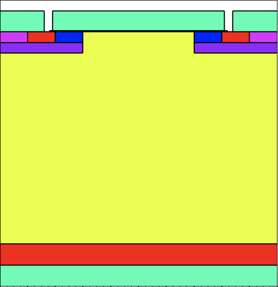
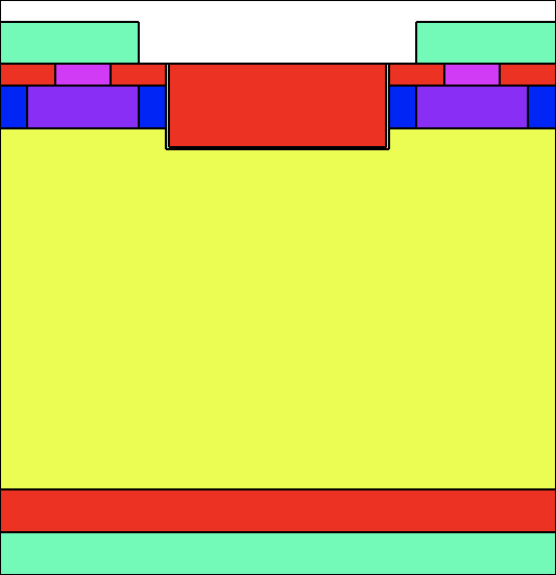
In this paper, two commercial 1.2kV SiC MOSFET devices were selected as research objects, and their simulation analysis was conducted. In order to test their dynamic switching characteristics at normal temperature, the static characteristics were simulated and analyzed at normal temperature to confirm the validity of the simulation models. The two types of SiC MOSFETs are planar gate and trench gate respectively,and the structures are shown in Fig.1. In order to study the difference between planar gate and trench gate structures themselves, two traditional structure are picked up, that carrier storage layer and p-buried layer under the gate are not used.
|
|
(a) | (b) |
Figure 1. The structure of (a) planar gate SiC MOSFET (b) trench gate SiC MOSFET. | |
In the vertical device, its gate is on the top of the device, while the drain is at the bottom of it. When the MOSFET is on, the current mainly flow vertically and the channel is formed in the P body between the P source and the N-drift. The doping concentration and thickness of the N-drift region and the device size of the two MOSFETs remain the same to ensure the reliability of the experiment. These important parameters are shown in the table below.
Table 1. Simulation parameters of the two MOSFETs.
Gate oxide thickness | Channel length | Drift thickness | N-drift doping concentration | |
parameters | 50nm | 1µm | 10µm | 5e15cm-3 |
In the process of device simulation, the physical models and device parameters used will affect the results of the whole experiment. For conventional silicon-based devices, the simulation process has been relatively mature, but in the simulation of SiC devices, the physical model based on silicon-based devices is not so accurate, its physical models need to be adjusted. In order to better simulate and analyze SiC devices, the Fermi-Dirac statistic was adopted in this paper to analyze the properties of materials with high doping concentration [10]. In terms of mobility, energy is lost due to various scattering processes after the activation of holes and electrons. In order to accurately describe these situations, Lombardi CVT Model is adopted in this paper. The Lombardi(CVT) model includes doping concentration factor as well as temperature effects and also accounts for the transverse electric fields, and the models to transverse electric fields in which ionized impurity scattering, carrier scattering, and high field degradation are transverse electric fields are included in the simulation calculation [11].
3. Measured results of the static characteristics
After the above physical models are adopted, the static electrical characteristics of the two devices are tested, and results are shown in the figure below.
|
Figure 2. Comparison of breakdown voltage between simulated planar gate MOSFET and commercial device. |
|
Figure 3. Comparison of breakdown voltage between simulated trench gate MOSFET and commercial device. |
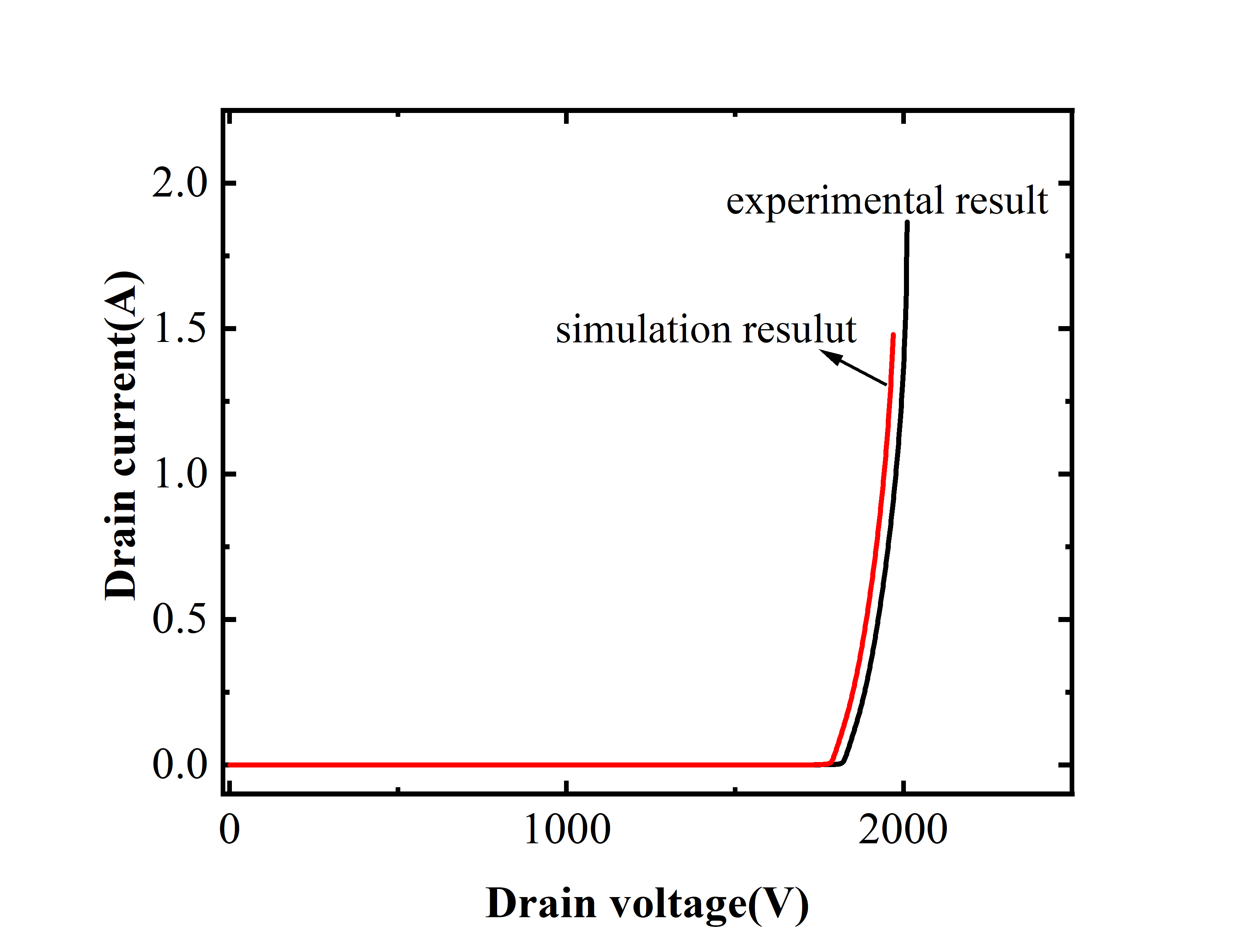
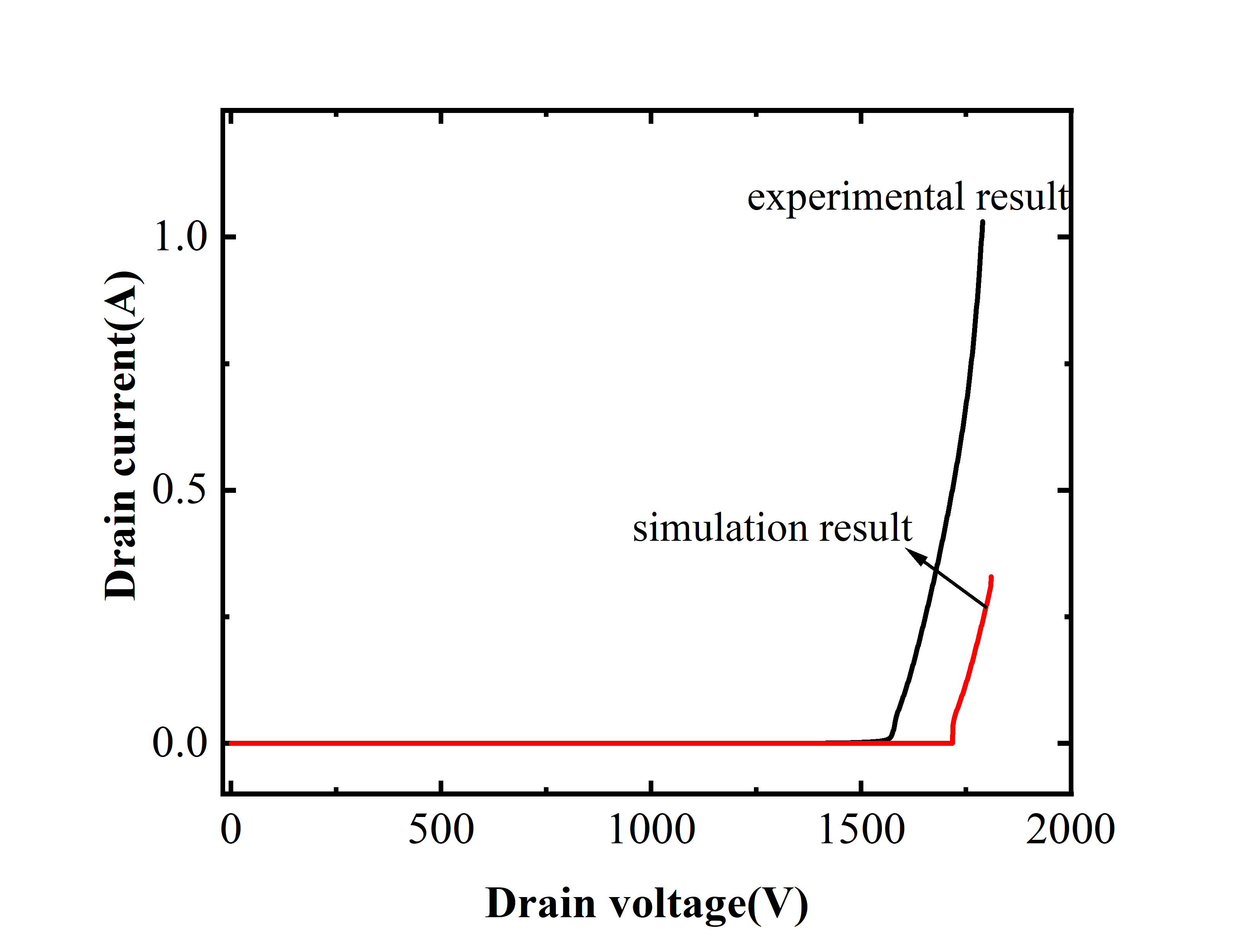
Fig.2 and Fig.3 show the breakdown characteristics of planar and trench gate SiC MOSFET between commercial ones.As can be seen, the breakdown voltage of simulated structure are similar to commercial structures, which shows that the using physical models are accurate. As shown in the figure, with the same thickness of N-drift and doping concentration, the breakdown voltage of the trench type structure will be lower than that of the planar type structure. This is because a larger voltage will be applied to the drain during off-state, and the electric field will gather at the corner below the trench. This will cause the electric field intensity of the oxide layer in the trench corner to be too large, which will make the device breakdown in advance. In order to increase the breakdown voltage of trench gate SiC MOSFET on the premise of ensuring the device conduction characteristics, the most commonly used method is not to reduce the doping concentration in the N- drift region, but to set a P-type region under the trench to protect the oxide layer [12].
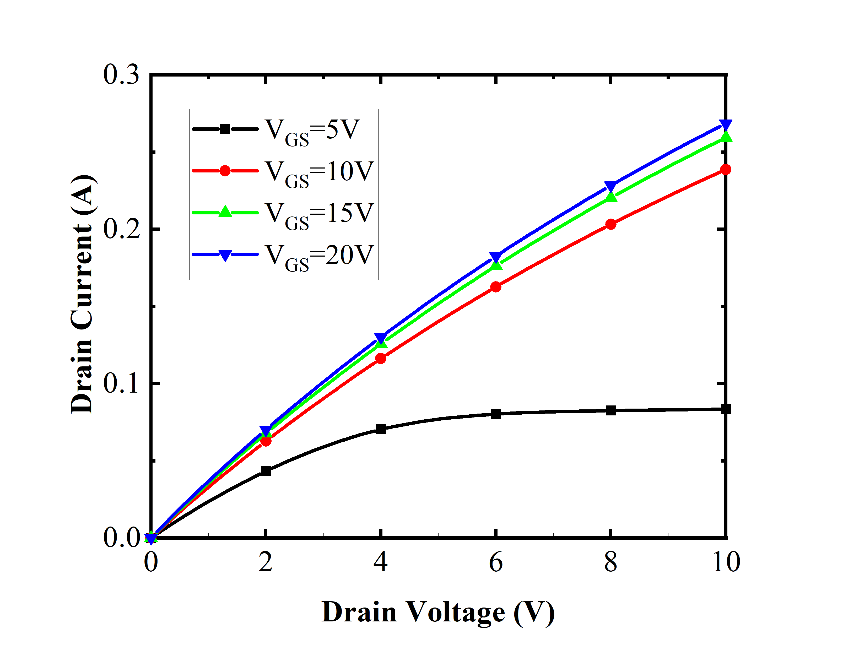
|
(a) |
|
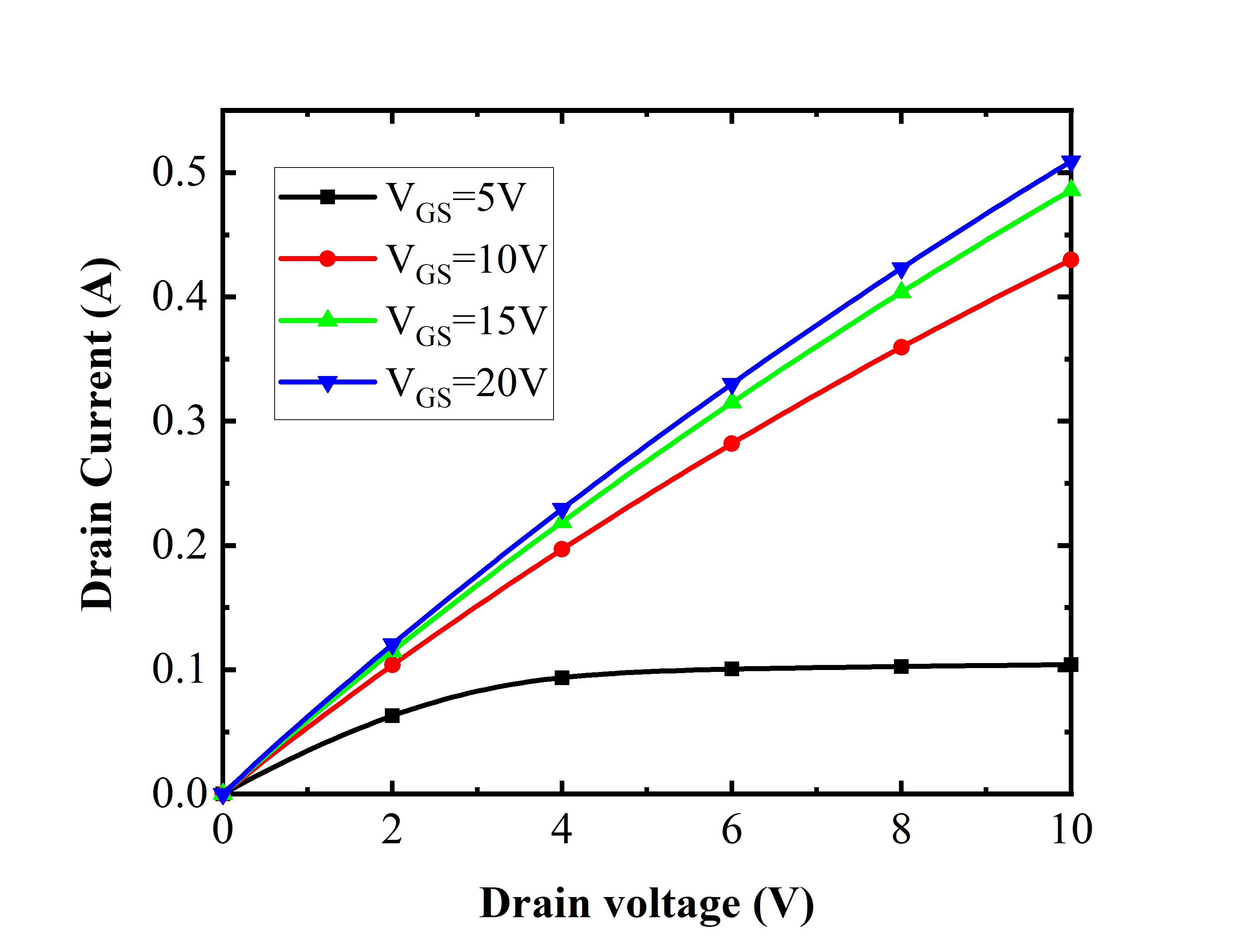
(b) |
Figure 4. (a) the conductivity characteristics of planar gate SiC MOSFET (b) the conductivity characteristics of trench gate SiC MOSFET. |
|
Figure 5. Comparison of transfer characteristics between planar gate MOSFET and trench gate MOSFET. |
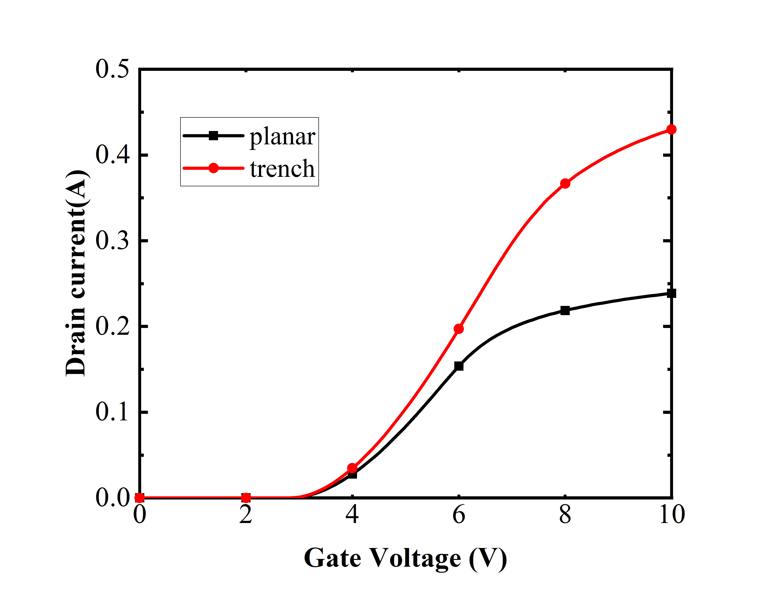
Fig. 4 (a) and (b) show the conduction characteristics of the planar gate and the trench gate SiC MOSFET respectively. At the same temperature, the conductivity of the trench type structure are much higher than the planar one, because under the same size of structure, the current flow path of the trench structure is shorter, while the planar structure has JFET resistance and accumulation layer resistance because of its JFET region, resulting in its poor conduction characteristics. Fig. 5 shows the transfer characteristic curves of the two structures.
4. Dynamic characteristics simulation
4.1. Introduction and analysis of double pulse circuit
Double pulse test is widely used in the characteristic evaluation of power switching elements such as MOSFET and IGBT. Many dynamic parameters of power devices can be obtained from the device data manual, but the device manual only gives the dynamic parameters under specific test conditions. When the parameters such as power circuit voltage and current, drive circuit voltage, resistance and external capacitance change, the switching time of the device will also change. Therefore, it is necessary to conduct double pulse test for specific operating conditions of the device during design to obtain more real performance.
In the dual pulse circuit, the test board is the core to complete the dual pulse test. It is generally a half bridge circuit, and sometimes the topology based on the actual system application is used. Its main components include bus capacitor and drive circuit. The bus capacitor provides stable bus voltage and required current for the test process. The drive circuit controller completes the switching action to achieve a double pulse process. For convenience, some parameters in the simulation design are expressed as follows: gate series resistance Rg, gate voltage VG, drain voltage Vg, load current IL, MOS gate-source voltage Vgs, MOS drain-source voltage Vds, MOS drain-source current Ids, and inductive load L. This paper uses a normal double pulse test circuit is shown in the figure below[13].
|
Figure 6. The double pulse test circuit. |
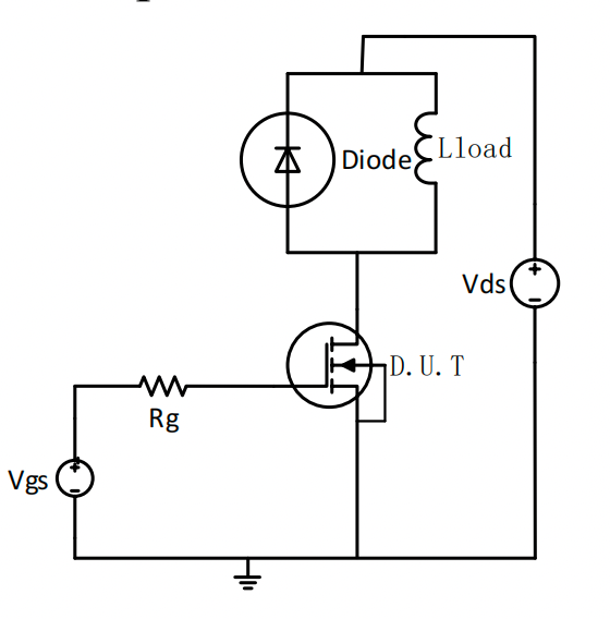
This test is used to detect the dynamic operating characteristics of the device under certain conditions. The high-voltage DC bias voltage VDS used in this paper is 400V, the gate series resistance is 5 Ω, and the drive voltage is 0/20V. The diode used in the simulation is an ideal diode. When testing planar gate and trench gate devices with different conduction characteristics so as to ensure the accuracy of the test, the inductance needs to be designed separately, because the inductance meets the following formula (1) during the test.
\( \frac{L{d_{i}}}{{d_{t}}}={V_{ds}} \) (1)
The cycle of a pulse is 4µs, and the current change time dt is 2µs. The current density of the two devices is set the same as 200A/cm2, so the inductance is 40µH.
4.2. Calculation of switching loss
The loss of MOSFET is mainly divided into dynamic operation loss and static operation loss. The static operation loss mainly refers to the loss between the conduction voltage drop and current when the device is in the conduction state. This paper mainly studies the dynamic loss, that is, the loss when the voltage and current change during the switching-on and switching-off of MOSFET. The switching loss is calculated using the measured drain-source voltage (Vds) and current (Ids) waveform. The expressions of the opening and closing losses are using formula (2), (3).
\( {E_{on}}=\int _{Ton}({V_{ds}}{I_{ds}})dt \) (2)
\( {E_{on}}=\int _{Toff}({V_{ds}}{I_{ds}})dt \) (3)
Eon, Eoff is the switching-on loss and the switching-off loss,Vds is the drain-source voltage, Ids is the drain-source current.
The integration time starts from the moment when the Vds rises to 10% of its specified value and ends when the collector current Ids drops to 2% of its specified value (this is the Eoff, while the Eon is the opposite).
4.3. Double pulse test results
The figure below illustrates the comparison between the switching-off and switching-on losses of the planar gate SiC MOSFET and the trench gate SiC MOSFET. The trench one has higher switching-off and switching-on consumption, 43.8% and 46.2% higher than the planar gate respectively.
|
(a) |
|
(b) |
Figure 7. The comparison of (a) switching-off characteristics and (b) switching-on characteristics between planar gate MOSFET and trench gate MOSFET. |
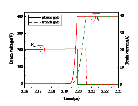
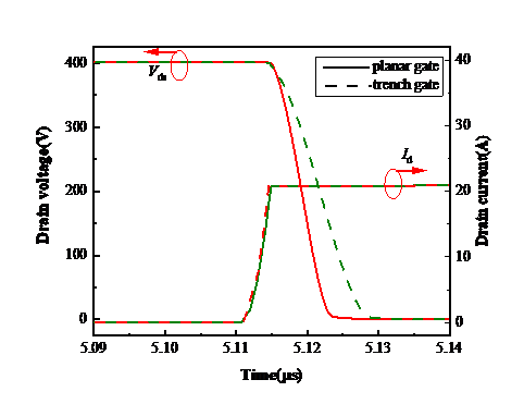
The current amplitude is 20A. It can be seen that the switching loss of MOSFET with trench type structure is larger than that of planar type when the device size is the same, which is consistent with the predicted result. This is because the internal capacitance is dominant in switching characteristics of MOSFET. However, for the trench gate, due to the large gate area, its gate source capacitance Cgs and gate drain capacitance Cgd are large, which makes the grid charge higher, damages the driving and switching characteristics, and ultimately leads to large switching loss of the device as a whole.
5. Conclusion
In this paper, two types of 1.2kV SiC MOSFETs are simulated respectively. Based on the simulation of silicon based MOSFETs, the models that can more accurately describe SiC devices are applied, and the static characteristics of two commercial MOSFETs are compared to verify the accuracy of the models. In terms of static characteristics, the two devices have the same N- drift region with the same thickness and doping concentration. The breakdown characteristics of the trench gate device are slightly smaller than that of the planar one, while the conduction characteristics are 50% higher than that of the planar gate structure. In addition, based on TCAD software, double pulse test is used to compare dynamic switching characteristics of planar gate and trench gate structures. The parameters of the test circuit are carefully studied to determine that the two devices have the same current density during the switching process. At the same operating temperature, the trench gate has higher switching loss, which is because the charging process of the device is slow due to the large capacitance. The above research results explore the simulation research of SiC MOSFET, which can be used as the theoretical basis for subsequent research.
References
[1]. J.W.Palmour et al.,“Silicon Carbide Power MOSFETs Breakthrough Performance from 900 V up to 15 kV”,International Symposium on Power Semiconductor Devices and IC’s (ISPD), 2014.
[2]. J. L. Hudgins, G. S. Simin, E. Santi, and M. A. Khan, "An assessment of wide bandgap semiconductors for power devices," IEEE Transactions on Power Electronics, vol. 18, no. 3, pp. 907-914, 2003.
[3]. L. D. Stevanovic, K. S. Matocha, P. A. Losee, J. S. Glaser, J. J. Nasadoski, and S. D. Arthur, "Recent advances in silicon carbide MOSFET power devices," in Applied Power Electronics Conference and Exposition (APEC), 2010 Twenty-Fifth Annual IEEE, 2010, pp. 401-407: IEEE.
[4]. J. Millan, P. Godignon, X. Perpi na, A. Perez-Tomas, and J. Rebollo,“A survey of wide bandgap power semiconductor devices,” IEEE Trans.Power Electron.,May 2014, vol. 29, no. 5, pp. 2155–2163.
[5]. M. Östling, R. Ghandi, and C.-M. Zetterling, "SiC power devices—Present status, applications and future perspective," in Power Semiconductor Devices and ICs (ISPSD), 2011 IEEE 23rd International Symposium on, 2011, pp. 10-15: IEEE.
[6]. Y. Baba, N. Matuda, S. Yawata, S. Izumi, N. Kawamura and T. Kawakami, "High reliability UMOSFET with oxide-nitride complex gate structure," Proceedings of 9th International Symposium on Power Semiconductor Devices and IC's, 1997, pp. 369-372, doi: 10.1109/ISPSD.1997.601520.
[7]. Ganesan P, Manju R, Razila K R and R. J. Vijayan, "Characterisation of 1200V, 35A SiC Mosfet using double pulse circuit," 2016 IEEE International Conference on Power Electronics, Drives and Energy Systems (PEDES), 2016, pp. 1-6, doi: 10.1109/PEDES.2016.7914225.
[8]. S. R. El-Helw, J. P. Kozak, R. Burgos, K. Ngo and D. Boroyevich, "Static and Dynamic Characterization of a 2.5 kV SiC MOSFET," 2018 IEEE 6th Workshop on Wide Bandgap Power Devices and Applications (WiPDA), 2018, pp. 199-203, doi: 10.1109/WiPDA.2018.8569044.
[9]. K. Matsui, R. Aiba, H. Yano, N. Iwamuro, M. Baba and S. Harada, "Comprehensive Study on Electrical Characteristics in 1.2 kV SiC SBD-integrated Trench and Planar MOSFETs," 2021 33rd International Symposium on Power Semiconductor Devices and ICs (ISPSD), 2021, pp. 215-218, doi: 10.23919/ISPSD50666.2021.9452287.
[10]. Yu, Z., and R.W. Dutton, "SEDAN III-A Generalized Electronic Material DeviceAnalysis Program", Stanford Electronics Laboratory Technical Report, Stanford University, July 1985
[11]. Lombardi et al, "A Physically Based Mobility Model for Numerical Simulation of Non-Planar Devices", IEEE Trans. on CAD, pp. 1164, Nov. 1988.
[12]. Kagawa, Yasuhiro & Fujiwara et al. (2014). 4H-SiC trench MOSFET with bottom oxide protection. Materials Science Forum. 778-780. 919-922.
[13]. H. Chen, J. Hao, Q. Zhou, Q. Feng and Y. Bai, "The Characteristics and Modeling of 600V and 1200V SiC Power MOSFET," 2018 14th IEEE International Conference on Solid-State and Integrated Circuit Technology (ICSICT), 2018, pp. 1-3, doi: 10.1109/ICSICT.2018.8564913.
Cite this article
Che,H. (2023). Simulation study on dynamic characteristics of SiC MOSFET. Theoretical and Natural Science,5,803-812.
Data availability
The datasets used and/or analyzed during the current study will be available from the authors upon reasonable request.
Disclaimer/Publisher's Note
The statements, opinions and data contained in all publications are solely those of the individual author(s) and contributor(s) and not of EWA Publishing and/or the editor(s). EWA Publishing and/or the editor(s) disclaim responsibility for any injury to people or property resulting from any ideas, methods, instructions or products referred to in the content.
About volume
Volume title: Proceedings of the 2nd International Conference on Computing Innovation and Applied Physics (CONF-CIAP 2023)
© 2024 by the author(s). Licensee EWA Publishing, Oxford, UK. This article is an open access article distributed under the terms and
conditions of the Creative Commons Attribution (CC BY) license. Authors who
publish this series agree to the following terms:
1. Authors retain copyright and grant the series right of first publication with the work simultaneously licensed under a Creative Commons
Attribution License that allows others to share the work with an acknowledgment of the work's authorship and initial publication in this
series.
2. Authors are able to enter into separate, additional contractual arrangements for the non-exclusive distribution of the series's published
version of the work (e.g., post it to an institutional repository or publish it in a book), with an acknowledgment of its initial
publication in this series.
3. Authors are permitted and encouraged to post their work online (e.g., in institutional repositories or on their website) prior to and
during the submission process, as it can lead to productive exchanges, as well as earlier and greater citation of published work (See
Open access policy for details).
References
[1]. J.W.Palmour et al.,“Silicon Carbide Power MOSFETs Breakthrough Performance from 900 V up to 15 kV”,International Symposium on Power Semiconductor Devices and IC’s (ISPD), 2014.
[2]. J. L. Hudgins, G. S. Simin, E. Santi, and M. A. Khan, "An assessment of wide bandgap semiconductors for power devices," IEEE Transactions on Power Electronics, vol. 18, no. 3, pp. 907-914, 2003.
[3]. L. D. Stevanovic, K. S. Matocha, P. A. Losee, J. S. Glaser, J. J. Nasadoski, and S. D. Arthur, "Recent advances in silicon carbide MOSFET power devices," in Applied Power Electronics Conference and Exposition (APEC), 2010 Twenty-Fifth Annual IEEE, 2010, pp. 401-407: IEEE.
[4]. J. Millan, P. Godignon, X. Perpi na, A. Perez-Tomas, and J. Rebollo,“A survey of wide bandgap power semiconductor devices,” IEEE Trans.Power Electron.,May 2014, vol. 29, no. 5, pp. 2155–2163.
[5]. M. Östling, R. Ghandi, and C.-M. Zetterling, "SiC power devices—Present status, applications and future perspective," in Power Semiconductor Devices and ICs (ISPSD), 2011 IEEE 23rd International Symposium on, 2011, pp. 10-15: IEEE.
[6]. Y. Baba, N. Matuda, S. Yawata, S. Izumi, N. Kawamura and T. Kawakami, "High reliability UMOSFET with oxide-nitride complex gate structure," Proceedings of 9th International Symposium on Power Semiconductor Devices and IC's, 1997, pp. 369-372, doi: 10.1109/ISPSD.1997.601520.
[7]. Ganesan P, Manju R, Razila K R and R. J. Vijayan, "Characterisation of 1200V, 35A SiC Mosfet using double pulse circuit," 2016 IEEE International Conference on Power Electronics, Drives and Energy Systems (PEDES), 2016, pp. 1-6, doi: 10.1109/PEDES.2016.7914225.
[8]. S. R. El-Helw, J. P. Kozak, R. Burgos, K. Ngo and D. Boroyevich, "Static and Dynamic Characterization of a 2.5 kV SiC MOSFET," 2018 IEEE 6th Workshop on Wide Bandgap Power Devices and Applications (WiPDA), 2018, pp. 199-203, doi: 10.1109/WiPDA.2018.8569044.
[9]. K. Matsui, R. Aiba, H. Yano, N. Iwamuro, M. Baba and S. Harada, "Comprehensive Study on Electrical Characteristics in 1.2 kV SiC SBD-integrated Trench and Planar MOSFETs," 2021 33rd International Symposium on Power Semiconductor Devices and ICs (ISPSD), 2021, pp. 215-218, doi: 10.23919/ISPSD50666.2021.9452287.
[10]. Yu, Z., and R.W. Dutton, "SEDAN III-A Generalized Electronic Material DeviceAnalysis Program", Stanford Electronics Laboratory Technical Report, Stanford University, July 1985
[11]. Lombardi et al, "A Physically Based Mobility Model for Numerical Simulation of Non-Planar Devices", IEEE Trans. on CAD, pp. 1164, Nov. 1988.
[12]. Kagawa, Yasuhiro & Fujiwara et al. (2014). 4H-SiC trench MOSFET with bottom oxide protection. Materials Science Forum. 778-780. 919-922.
[13]. H. Chen, J. Hao, Q. Zhou, Q. Feng and Y. Bai, "The Characteristics and Modeling of 600V and 1200V SiC Power MOSFET," 2018 14th IEEE International Conference on Solid-State and Integrated Circuit Technology (ICSICT), 2018, pp. 1-3, doi: 10.1109/ICSICT.2018.8564913.