


1. Introduction
MOSFETs are integrated circuits' fundamental building blocks, essential in switching and amplifying virtually all digital logic, memory, and analog systems. Their compact dimensions and low power consumption have long driven the continuous scaling of very large-scale integration (VLSI). However, as device geometries shrink to 5 nm and below, conventional single-gate MOSFETs encounter pronounced limitations, including severe short-channel effects (SCEs), increased leakage currents, and diminished gate electrostatic control [1].
To overcome these challenges, multigate device architectures such as double-gate (DG), FinFET, and gate-all-around (GAA) MOSFETs have been developed [2]. The DG-MOSFET can be recognized as a transitional stage between single-gate MOSFETs and FinFETs. DG MOSFETs are irreplaceable because of the mature technology, low cost, and energy conservation, which means they are essential in low-power circuits. If they overcome challenges by redesigning their structure, the DG MOSFETs can be cheaply applied to more demanding circuits. Furthermore, two gates perform better for enhancing electrostatic control of the channel [3], with recent studies demonstrating notable suppression of short-channel effects (SCEs) through the integration of two-dimensional materials [1]. Based on DG MOSFETs’ structure, variants such as DMDG MOSFETs, strained DG MOSFETs, and gate-stacked DG MOSFETs have been proposed to refine threshold voltage control further, improve subthreshold swing, and so on [4, 5]. Within this framework, gate-stacking—using a multilayer dielectric stack instead of a single SiO₂ layer—has become a central research focus. This review concentrates on gate-stacking, particularly emphasizing how material innovations and device engineering can be leveraged to optimize its performance further.
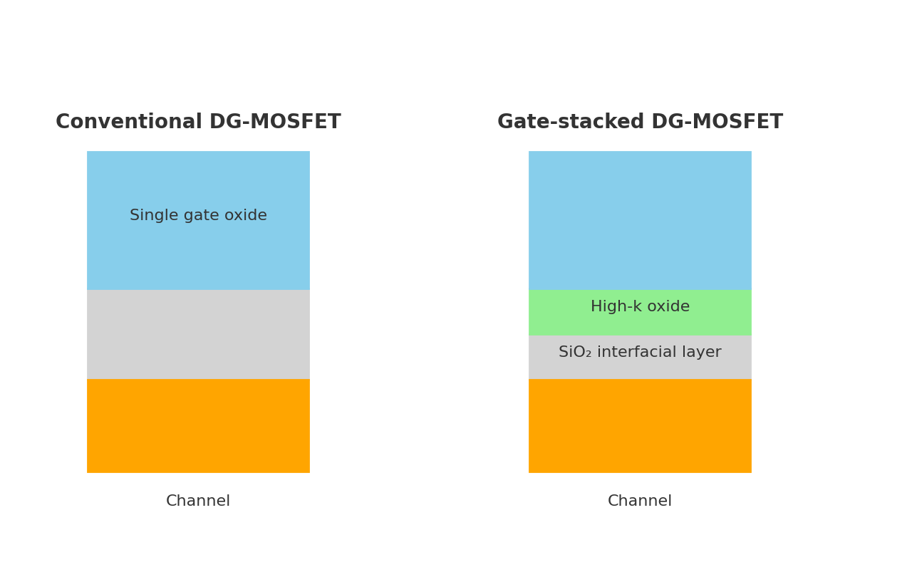
As illustrated in Figure 1, it is clear that gate stacking typically combines a thin SiO₂ interfacial layer with a high-k dielectric, simultaneously preserving interface quality and enhancing gate control [6, 7]. This approach benefits logic circuits and extends to biosensing and ultra-low-power applications [8,9]. Moreover, studies on trigate and nanowire-based devices suggest further opportunities through integrating structural and material engineering [10,11].
Current research faces scaling challenges: although FinFETs alleviate short-channel effects (SCEs), they cannot fully suppress them at deeply scaled nodes [2]. At the same time, gate-all-around (GAA) transistors offer superior electrostatic control but incur excessive fabrication cost and complexity. The gate-stacking structure has been introduced to address these issues and enhance DG-MOSFETs' performance [3, 6]. Nevertheless, reliance on a single technological approach remains insufficient. While gate-stacking effectively mitigates SCEs and improves device characteristics, it cannot be absolutely eradicated and simultaneously introduces new challenges, including elevated interface trap density and band alignment concerns [12, 13].
Considering these factors, this review introduces the structural development of gate-stacked DG-MOSFETs, evaluating their capability to suppress SCEs, and addressing their inherent limitations. Distinct from prior surveys, we emphasize the innovative perspective that further progress relies on integrating gate-stacking with complementary optimization strategies, including exploring diverse high-k dielectrics, incorporating strain engineering, and adopting dual-material gate concepts [14]. Such synergistic approaches strengthen the intrinsic benefits of gate-stacking and provide new avenues to refine threshold voltage control, enhance subthreshold swing, and boost device scalability. Building on structural advances and material/process innovations, this review outlines a roadmap toward more stable, energy-efficient, and versatile DG-MOSFET platforms for next-generation CMOS technologies [10, 11].
2. Evolution of gate-stacking structures
2.1. Gate-stacking concept
As MOSFETs scaled down to the nanoscale, traditional gate structures—once sufficient at larger dimensions—became inadequate for controlling channel conduction. With channel lengths approaching the scale of depletion regions, SCEs emerged [1, 6].
In single-gate MOSFETs, this lowers source barriers, allowing carrier injection even in the “off” state, which increases leakage current, raises static power consumption, and degrades logic state distinction [7,12,13]. Strengthening electrostatic control is thus critical to suppress drain-induced barrier lowering (DIBL) and related SCEs. Double-gate (DG) MOSFETs mitigate these issues using two gates to enhance gate–channel coupling [3,4,11]. However, residual SCEs and reliability challenges remain. To further enhance control, DG-MOSFETs have evolved to adopt gate-stacked dielectric structures, incorporating multilayer dielectrics for improved electrostatic performance [6, 7].
Compared with conventional DG MOSFETs, gate-stacked DG MOSFETs differ in the gate dielectric by adding a high-k layer on top of SiO₂ [5,6,10]. Because a high-k material is more easily polarized, the equivalent oxide thickness (EOT) becomes smaller than that of SiO₂ at comparable physical thickness. Viewing the gate, gate dielectric, and channel as a capacitor, Cox follows the same relation:
which directly links larger permittivity (high-k) or smaller effective thickness (EOT) to a higher Cox [6, 10].
By analogy with a parallel-plate capacitor, an increase in the gate-oxide capacitance Cox leads, for a given gate voltage VGS , to a larger induced inversion charge in the channel. Consequently, the channel carrier density and the drain current ID increase; this effect is often accompanied by a reduction in the device threshold voltage Vth, producing several practical advantages.
A lower Vthenables the transistor to switch on at a smaller gate voltage (
This expression captures these relationships:
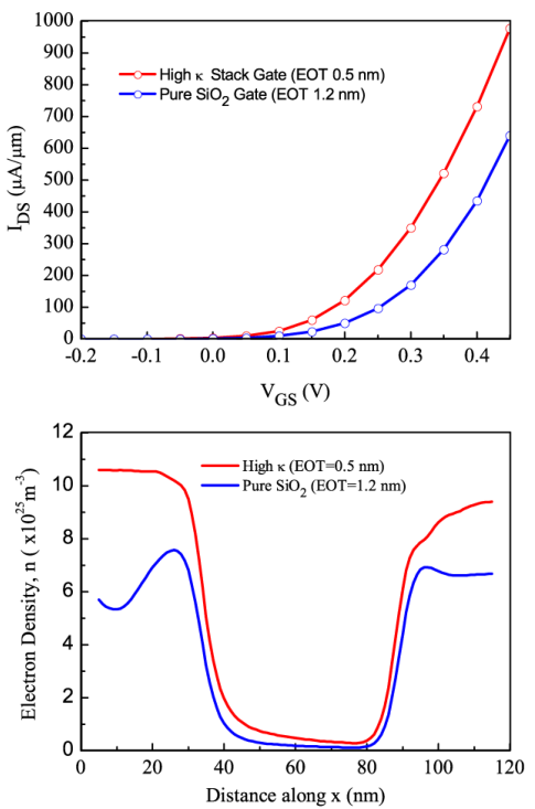
(a) The high-κ stack (EOT = 0.5 nm) exhibits higher Ion than pure SiO₂ (EOT = 1.2 nm), indicating enhanced drive current and reduced Vth due to increased Cox.
(b) Electron density along the channel is higher in the high-κ stack device, confirming improved gate control.
Figure 2 demonstrates the core mechanism: EOT ↓ ⇒ Cox↑ ⇒ Vth↓ ⇒ Ion↑, supporting the performance advantage of gate-stacked DG-MOSFETs.
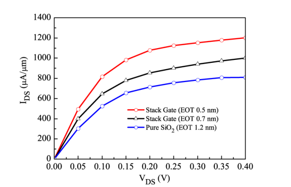
In Figure 3, Vth decreases as EOT reduces from 1.2 nm (SiO₂) to 0.7 nm and 0.5 nm (high-κ stacks), confirming stronger gate control.
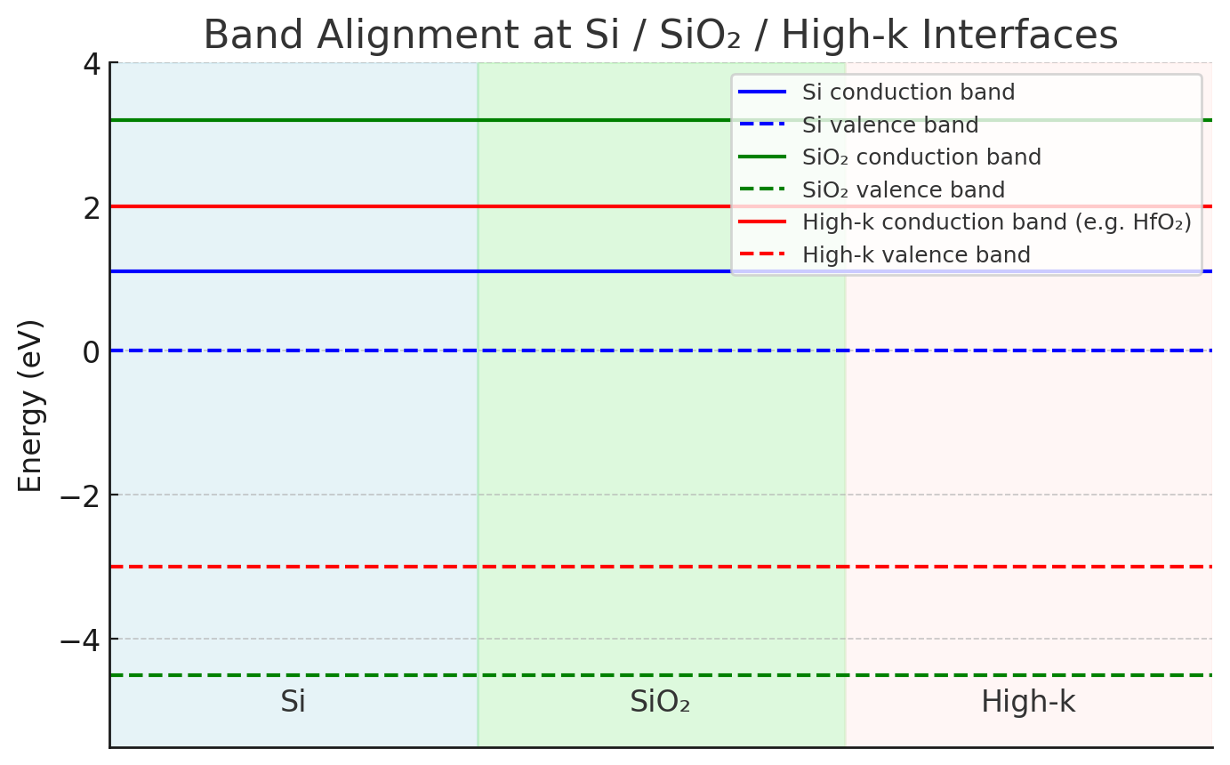
Despite the advantages of high-κ materials, a thin SiO₂ interfacial layer is typically retained to address challenges such as high interface-state density, poor band alignment with silicon, and process immaturity [7,10]. Band alignment is critical for minimizing gate leakage and ensuring device reliability. SiO₂ provides favorable conduction and valence band offsets, effectively suppressing unwanted carrier tunneling [6,7], which explains its continued use as a foundational layer in gate-stacked DG-MOSFETs that shows evidently in Figure 4. This integration balances high-κ dielectrics' benefits with traditional interfaces' stability, forming a key part of current optimization strategies.
Above all, gate stacking has proven highly effective in mitigating short-channel effects by reducing EOT, enhancing gate capacitance and drive current, and lowering the threshold voltage. However, further optimization remains possible, particularly in addressing performance limitations through improved material selection and structural engineering. The following section focuses on analyzing key performance metrics to identify critical factors and guide the development of more efficient and reliable gate-stacked DG-MOSFETs.
2.2. Material choices
Several viable high-k dielectric candidates exist, including HfO₂, Al₂O₃, ZrO₂, and La₂O₃. As noted earlier, the primary selection criterion is the ability to reduce the equivalent oxide thickness (EOT) while maintaining acceptable leakage. In a study by Farzana et al. [6], the optimal gate-stacking structure was investigated using a quantum ballistic transport model. Their work focused on a fully depleted n-type DG-MOSFET, with the top gate employing a SiO₂/La₂O₃ stack, a 4 nm bottom oxide, and an intrinsic silicon channel. The source/drain doping was set to 2×1020 cm-3, the silicon film thickness to tSi=2.5 nm, and the metal gate work function to 4.2 eV.
Furthermore, Salmani-Jelodar et al. [7] stressed that, for a fixed EOT = 0.86 nm, the optimum interface oxide thickness depends on the dielectric constant of the high-k layer: Al₂O₃ requires ≈3 Å SiO₂, HfO₂ ≈5 Å, and La₂O₃ ≈7 Å to balance leakage suppression and electrostatic control.
For comparison, the minimum usable top oxide thickness in a conventional SiO₂-only device is about 1.2 nm, below which gate tunneling becomes prohibitive. By contrast, high-k gate stacks achieve much smaller effective EOT values (≈0.7–0.5 nm, as derived from equations (3)) without sacrificing leakage performance, owing to their larger physical thickness.
|
High-k Material |
Recommended SiO₂ Interfacial Layer |
ION (Drive Current) |
IOFF (Leakage Current) |
SS (Subthreshold Swing) |
DIBL |
IGate (Gate Tunneling) |
Overall Assessment |
|
Al₂O₃ (k≈9) |
≈ 3 Å |
Moderate to high, good drivability |
Very low, best among candidates |
Close to ideal |
Well suppressed |
Extremely low |
Most balanced, suitable for low-power applications |
|
HfO₂ (k≈ 20) |
≈ 5 Å |
High, significant improvement |
Well controlled |
Slightly higher than Al₂O₃ |
Relatively low, slight degradation |
Low |
Balanced choice, mainstream for high-performance nodes |
|
La₂O₃ (k≈ 30) |
≈ 7 Å |
Highest, strongest drivability |
Relatively high, leakage concern |
Noticeably degraded (due to thickness) |
Poor performance |
Low |
Suitable for extreme scaling exploration, but with reliability concerns |
As shown in Table 1, different high-κ dielectric materials present distinct trade-offs among drivability, leakage suppression, and short-channel control. Given that double-gate (DG) MOSFETs are predominantly used in low-power circuit applications, materials with low leakage currents and mature fabrication compatibility are particularly desirable. From this perspective, Al₂O₃ combined with a SiO₂ interfacial layer emerges as an optimal choice. This stack offers the most balanced characteristics, including near-ideal subthreshold swing (SS), extremely low gate tunneling current, and excellent electrostatic control, making it especially suitable for ultra-low-power applications and thus well aligned with the inherent advantages of DG MOSFETs.
Moreover, considering the potential for DG MOSFETs to be extended into HPC domains with reduced cost, HfO₂ and La₂O₃ present promising opportunities. Although La₂O₃ raises concerns related to interface reliability and increased leakage, its exceptionally high drive current indicates strong potential for performance-critical nodes with DG MOSFETs. These drawbacks may be addressed through complementary techniques, such as strain engineering and dual-material gate (DMG) integration, which have improved carrier mobility and electrostatic integrity.
2.3. Other promising structural optimization strategies
Beyond material selection, strain engineering and dual-material gate (DMG) design offer effective structural enhancements for gate-stacked DG-MOSFETs. Strain engineering improves carrier mobility by reducing effective mass, enhancing drive current, a critical advantage for high-speed and high-performance logic applications [5]. In parallel, the DMG structure introduces a step potential along the channel using two gate materials with different work functions, suppressing short-channel effects such as DIBL while enabling threshold voltage tuning without degrading drivability [4].
When combined with gate stacking, both techniques address complementary challenges. While gate stacking strengthens gate control and suppresses leakage and strain, DMG improves current transport and electrostatic modulation. This co-optimization boosts device performance and expands DG-MOSFET applicability—from low-power circuits to performance-driven systems and emerging domains like biosensing [7].
|
Module |
Recommended Structural Combination |
Synergistic Mechanism |
|
Channel Region |
Tensile strain (for nMOS) / Compressive strain (for pMOS) |
Enhances carrier mobility |
|
Gate Dielectric |
SiO₂ / HfO₂ stack (Gate-stacked structure) |
Reduces leakage, strengthens electrostatic control |
|
Gate Metal Layer |
TiN (source-side) / TaN (drain-side) — DMG structure |
Tailors potential distribution, suppresses DIBL |
|
Overall Objective |
High Ion, low Ioff, strong gate control, low power consumption |
Ideal for high-performance/low-power SoC core applications |
In Table 2, there are optimized structural strategy for gate-stacked DG-MOSFETs combining strain and DMG to enhance mobility, gate control, and short-channel suppression for advanced CMOS applications.
3. Performance optimization of gate-stacked double-gate MOSFETs
Building on the structural advantages of gate-stacked DG-MOSFETs, assessing how these design choices translate into measurable device performance is necessary. Key figures of merit—such as the on-state current (Ion), off-state leakage (Ioff), subthreshold swing (SS), and drain-induced barrier lowering (DIBL)—provide critical insight into the trade-offs between enhanced gate control and potential reliability challenges.
3.1. Improved subthreshold characteristics
The subthreshold swing (SS) in gate-stacked DG-MOSFETs can be significantly reduced—approaching the theoretical limit of ~60 mV/dec—thanks to enhanced gate electrostatics [6,7]. This improvement effectively suppresses short-channel effects and mitigates threshold voltage variation, enabling steeper switching characteristics [12], because
Such behavior is essential for low-power design, supporting reliable operation at reduced supply voltages. By achieving near-ideal SS through gate-stacking, these devices offer a compelling route toward energy-efficient CMOS technologies with potential applications in biosensing and ultra-low-power systems [8].
Regarding gate-stacking structure, high-κ gate stacks improve gate control, lowering the subthreshold swing from 74 mV/dec to 63 mV/dec [6] compared to conventional SiO₂ gates. Together, these results substantiate the logical chain: EOT ↓ ⇒ Cox↑ ⇒ Vth↓ ⇒ Ion↑,
A key aspect yet to be fully explained is how an increased gate oxide capacitance Cox contributes to lowering the Vth.
This formula can actually expound the logic there.
Among these, lowering Vth also increases the transistor’s sensitivity in the subthreshold region: the device responds more strongly to small changes in gate voltage. This property can be exploited in ultra-low-power sensing applications (e.g., biosensors) to improve sensitivity and detection accuracy [8].
3.2. Reduced leakage current
Reducing leakage current can help us improve the performance of the MOSFET in our design and optimization. More specifically, the tunneling current accounts for a significant proportion of the leakage current, which is the kernel problem for the gate-stacking structure to address.
As stated before, when the gate dielectric is replaced with the high-k material, the EOT declines, but physical thickness augments [6], which addresses the tunneling current. In that way, the tunneling current will nearly disappear when the dielectric's physical thickness is enough.
If the SiO2 layer's thickness is less than 1.2nm, electrons will penetrate the whole layer, and the tunneling current will dominate.
Another essential part of the leakage current is the subthreshold current. Among the various leakage components in scaled MOSFETs, the subthreshold current is often dominant, especially when the gate voltage is below the threshold voltage. In this regime, carriers are still thermally activated to overcome the potential barrier, giving rise to an exponential dependence of the drain current on the gate bias:
A steeper subthreshold swing (SS) therefore suppresses subthreshold leakage by reducing the slope of this exponential relationship [7]. Due to their enhanced gate control and reduced EOT, gate-stacked DG-MOSFETs effectively lower subthreshold leakage compared with single-gate counterparts [6]. This improvement reduces static power consumption and enables reliable operation in low-power circuits and sensing applications, where leakage currents are critical design constraints [8].
3.3. Increased drive current (Ion)
As discussed earlier, enhancing the drive current (Ion) is a core motivation behind adopting gate-stacked structures in DG-MOSFETs. By reducing the equivalent oxide thickness (EOT), high-κ dielectrics increase the gate capacitance (Cox), which directly strengthens the gate–channel coupling and enables more carriers to flow during the on-state. Physically, Ion represents the current conducted by electrons or holes per unit time when the device is active—thus, a higher drive current implies faster charge/discharge cycles within the transistor.
At the circuit level, switching delay is inversely proportional to Ion, as expressed by
Therefore, increasing
Furthermore, strain engineering can be integrated to reduce carrier effective mass and boost mobility [5], providing an additional pathway to enhance Ion. High-performance computing (HPC) applications benefit significantly from such improvements, where rapid logic switching is essential. Meanwhile, in ultra-low-power domains, a higher Ion under constant
4. Application fields of gate-stacked double - gate MOSFETs
Gate-stacked DG-MOSFETs, benefiting from enhanced gate control and reduced leakage, present a highly adaptable platform for low-power and high-performance applications. In ultra-low-power electronics, suppressing subthreshold swing and gate leakage enables reliable operation at reduced supply voltages, making these devices ideal for battery-constrained systems, such as portable electronics and IoT sensors [6,7,9]. Simultaneously, when integrated with strain engineering, gate-stacked DG-MOSFETs achieve significant improvements in carrier mobility and drive current, offering a cost-effective solution for high-performance computing (HPC) scenarios that demand rapid charge/discharge cycles and high-speed logic switching [5].
Beyond digital logic, their steep subthreshold characteristics make them well-suited for biosensing applications, where sensitivity to minute voltage changes is critical for detection accuracy. For example, Singh et al. [8] demonstrate that gate-stacked configurations significantly enhance biosensor transduction efficiency by amplifying low-amplitude signals. Moreover, gate-stacking compatibility with emerging multigate architectures—such as FinFETs and GAAFETs—ensures continued relevance in advanced technology nodes, facilitating scalable CMOS integration.
Looking forward, the optimization of gate-stacked DG-MOSFETs demands the selection of high-κ materials with favorable electrostatic and leakage characteristics and synergistic co-design strategies. These include integrating strain engineering, dual-material gates, and structural innovations like FinFET or DMDG architectures [4,5], which mitigate reliability issues such as interface trap density or band misalignment. While Al₂O₃ gate stacks offer a balanced solution for low-power use cases, HfO₂ and La₂O₃ variants unlock potential in performance-driven systems, albeit with trade-offs that require advanced co-optimization [7].
5. Future development trends of the gate-stacking structure
While gate-stacked DG-MOSFETs have shown impressive gains in short-channel control and leakage suppression, further refinements are needed to meet the demands of scalable and application-specific design. One critical direction is the judicious selection of high-κ materials for gate stacks. For instance, Al₂O₃ with a SiO₂ interfacial layer strikes an optimal balance—offering low leakage, ideal subthreshold swing, and compatibility with ultra-low-power logic, making it especially suitable for DG-MOSFET deployment in power-sensitive domains. Additionally, the dielectric stack must continue to evolve to address reliability and integration issues such as band alignment and interface quality.
Beyond materials, co-design strategies combining gate-stacking with strain and dual-material gate (DMG) techniques offer a path toward performance-driven customization. Strain enhances mobility; DMG improves potential distribution and suppresses DIBL; gate-stack boosts Cox and suppresses leakage. These effects align well with emerging application demands: for example, HPC circuits require high drive current and fast switching—both achievable via strained high- Cox stacks. Combining with material, La₂O₃, while presenting reliability and leakage challenges, stresses outstanding drive current, highlighting its potential in high-performance DG-MOSFET designs. Meanwhile, ultra-low-power designs benefit from steeper subthreshold slopes and lower Vth, realized through gate-stack–DMG synergy. In biosensing, the sharp SS directly enhances detection sensitivity. Future development should thus focus on integrated material–structure strategies.
6. Conclusion
This work systematically reviews the structural and material evolution of gate-stacked double-gate (DG) MOSFETs as a response to the scaling limits of conventional single-gate devices. By introducing stacked high-k/SiO₂ gate dielectrics, these transistors achieve reduced leakage, enhanced electrostatics, and improved figures of merit such as subthreshold swing, drain-induced barrier lowering, and drive current. Their applicability spans low-power circuits, high-performance computing, and biosensing, underscoring both breadth and technological relevance. Despite unresolved issues in interface quality, band alignment, and scalability at deep nanoscale nodes, the study stresses that gate-stacked DG-MOSFETs form a critical stepping stone toward next-generation CMOS. Their value lies in immediate performance benefits and compatibility with advanced architectures, ensuring a continuous pathway for semiconductor innovation.
References
[1]. X. Zhou, L. Yang, C. Liu, Y. Zhao, and K. Zhang, “Short-Channel Effect Suppression and Footprint Reduction in Double Gate-All-Around Field Effect Transistors and Inverters Based on Two-Dimensional Materials, ” ACS Appl. Electron. Mater., vol. 6, no. 7, pp. 3852–3861, Jul. 2024, doi: 10.1021/acsaelm.4c01319.
[2]. Y. Cui, Z. Zhong, and C. Wang, “High-k gate dielectrics for advanced MOS devices, ” Nat. Rev. Mater., vol. 6, pp. 131–148, 2021, doi: 10.1038/s41578-020-00243-4.
[3]. J. Saint-Martin, A. Bournel, and P. Dollfus, “Comparison of multiple-gate MOSFET architectures using Monte Carlo simulation, ” arXiv preprint cond-mat/0505168, May 2005. Available: https: //arxiv.org/abs/cond-mat/0505168.
[4]. G. V. Reddy and M. J. Kumar, “A New Dual-Material Double-Gate (DMDG) Nanoscale SOI MOSFET – Two-Dimensional Analytical Modeling and Simulation, ” arXiv, Aug. 2010.
[5]. P. K. Pradhan, S. K. Mohapatra, P. K. Sahu, and S. Parija, “Impact of Strain on Fully Depleted Strained Gate Stack Double-Gate (FD-S-GS-DG) MOSFET: A Simulation Study, ” ECTI Trans. Electr. Eng., Electron. Commun., vol. 17, no. 2, pp.--, 2024.
[6]. E. Farzana, S. Chowdhury, R. Ahmed, and M. Z. R. Khan, “Performance analysis of nanoscale double gate MOSFETs with high-k gate stack, ” Appl. Mech. Mater., vols. 110–116, pp. 1892–1899, Oct. 2011, doi: 10.4028/www.scientific.net/AMM.110-116.1892.
[7]. M. Salmani-Jelodar, H. Ilatikhameneh, S. Kim, K. Ng, and G. Klimeck, “Optimum high-k oxide for the best performance of ultra-scaled double-gate MOSFETs, ” arXiv preprint arXiv: 1502.06178, Feb. 2015. Available: https: //arxiv.org/abs/1502.06178.
[8]. S. K. Singh, R. Kumar, and P. K. Yadav, “Thermal influence on performance characteristics of double gate MOSFET biosensors with gate stack configuration, ” Discover Appl. Sci., vol. 6, no. 202, pp. 1–12, Aug. 2024, doi: 10.1007/s42452-024-06055-1.
[9]. G. Fiori and G. Iannaccone, “Ultralow-power tunnel FETs with high-k gate stacks for beyond-CMOS applications, ” IEEE Trans. Nanotechnol., vol. 10, no. 6, pp. 1409–1416, Nov. 2011, doi: 10.1109/TNANO.2011.2165073.
[10]. A. T. Shora, “3-D Modelling Based Comprehensive Analysis of High-κ Gate Stack Graded Channel Dual Material Trigate MOSFET, ” J. Semicond., vol. 39, no. 12, Art. 124016, 2018.
[11]. E. Dastjerdy, R. Ghayour, and H. Sarvari, “Simulation and Analysis of the Frequency Performance of a New Silicon Nanowire MOSFET Structure, ” Physica E: Low-Dimensional Systems and Nanostructures, vol. 45, pp. 66–71, Aug. 2012, doi: 10.1016/j.physe.2012.07.007.
[12]. H. Jung, “Analysis of subthreshold swing in junctionless double gate MOSFET using stacked high-k gate oxide, ” Int. J. Electr. Comput. Eng., vol. 11, no. 3, pp. 2522–2530, Jun. 2021, doi: 10.11591/ijece.v11i3.pp2522-2530.
[13]. K. Martens, A. Vandooren, S. Sioncke, and G. Groeseneken, “Performance projections for gate-stack engineered double-gate MOSFETs, ” IEEE Trans. Electron Devices, vol. 61, no. 12, pp. 4145–4152, Dec. 2014, doi: 10.1109/TED.2014.2365162.
[14]. Z. Dibi, R. Boujamaa, and A. Jarray, “New gate stack double diffusion MOSFET design to improve the electrical performances for power applications, ” Proc. World Acad. Sci. Eng. Technol., vol. 1, no. 11, pp. 617–621, 2007.
Cite this article
Wang,W. (2025). The Review of Structure Development of Gate-stacked Double-Gate MOSFETs. Theoretical and Natural Science,145,17-27.
Data availability
The datasets used and/or analyzed during the current study will be available from the authors upon reasonable request.
Disclaimer/Publisher's Note
The statements, opinions and data contained in all publications are solely those of the individual author(s) and contributor(s) and not of EWA Publishing and/or the editor(s). EWA Publishing and/or the editor(s) disclaim responsibility for any injury to people or property resulting from any ideas, methods, instructions or products referred to in the content.
About volume
Volume title: Proceedings of CONF-CIAP 2026 Symposium: International Conference on Atomic Magnetometer and Applications
© 2024 by the author(s). Licensee EWA Publishing, Oxford, UK. This article is an open access article distributed under the terms and
conditions of the Creative Commons Attribution (CC BY) license. Authors who
publish this series agree to the following terms:
1. Authors retain copyright and grant the series right of first publication with the work simultaneously licensed under a Creative Commons
Attribution License that allows others to share the work with an acknowledgment of the work's authorship and initial publication in this
series.
2. Authors are able to enter into separate, additional contractual arrangements for the non-exclusive distribution of the series's published
version of the work (e.g., post it to an institutional repository or publish it in a book), with an acknowledgment of its initial
publication in this series.
3. Authors are permitted and encouraged to post their work online (e.g., in institutional repositories or on their website) prior to and
during the submission process, as it can lead to productive exchanges, as well as earlier and greater citation of published work (See
Open access policy for details).
References
[1]. X. Zhou, L. Yang, C. Liu, Y. Zhao, and K. Zhang, “Short-Channel Effect Suppression and Footprint Reduction in Double Gate-All-Around Field Effect Transistors and Inverters Based on Two-Dimensional Materials, ” ACS Appl. Electron. Mater., vol. 6, no. 7, pp. 3852–3861, Jul. 2024, doi: 10.1021/acsaelm.4c01319.
[2]. Y. Cui, Z. Zhong, and C. Wang, “High-k gate dielectrics for advanced MOS devices, ” Nat. Rev. Mater., vol. 6, pp. 131–148, 2021, doi: 10.1038/s41578-020-00243-4.
[3]. J. Saint-Martin, A. Bournel, and P. Dollfus, “Comparison of multiple-gate MOSFET architectures using Monte Carlo simulation, ” arXiv preprint cond-mat/0505168, May 2005. Available: https: //arxiv.org/abs/cond-mat/0505168.
[4]. G. V. Reddy and M. J. Kumar, “A New Dual-Material Double-Gate (DMDG) Nanoscale SOI MOSFET – Two-Dimensional Analytical Modeling and Simulation, ” arXiv, Aug. 2010.
[5]. P. K. Pradhan, S. K. Mohapatra, P. K. Sahu, and S. Parija, “Impact of Strain on Fully Depleted Strained Gate Stack Double-Gate (FD-S-GS-DG) MOSFET: A Simulation Study, ” ECTI Trans. Electr. Eng., Electron. Commun., vol. 17, no. 2, pp.--, 2024.
[6]. E. Farzana, S. Chowdhury, R. Ahmed, and M. Z. R. Khan, “Performance analysis of nanoscale double gate MOSFETs with high-k gate stack, ” Appl. Mech. Mater., vols. 110–116, pp. 1892–1899, Oct. 2011, doi: 10.4028/www.scientific.net/AMM.110-116.1892.
[7]. M. Salmani-Jelodar, H. Ilatikhameneh, S. Kim, K. Ng, and G. Klimeck, “Optimum high-k oxide for the best performance of ultra-scaled double-gate MOSFETs, ” arXiv preprint arXiv: 1502.06178, Feb. 2015. Available: https: //arxiv.org/abs/1502.06178.
[8]. S. K. Singh, R. Kumar, and P. K. Yadav, “Thermal influence on performance characteristics of double gate MOSFET biosensors with gate stack configuration, ” Discover Appl. Sci., vol. 6, no. 202, pp. 1–12, Aug. 2024, doi: 10.1007/s42452-024-06055-1.
[9]. G. Fiori and G. Iannaccone, “Ultralow-power tunnel FETs with high-k gate stacks for beyond-CMOS applications, ” IEEE Trans. Nanotechnol., vol. 10, no. 6, pp. 1409–1416, Nov. 2011, doi: 10.1109/TNANO.2011.2165073.
[10]. A. T. Shora, “3-D Modelling Based Comprehensive Analysis of High-κ Gate Stack Graded Channel Dual Material Trigate MOSFET, ” J. Semicond., vol. 39, no. 12, Art. 124016, 2018.
[11]. E. Dastjerdy, R. Ghayour, and H. Sarvari, “Simulation and Analysis of the Frequency Performance of a New Silicon Nanowire MOSFET Structure, ” Physica E: Low-Dimensional Systems and Nanostructures, vol. 45, pp. 66–71, Aug. 2012, doi: 10.1016/j.physe.2012.07.007.
[12]. H. Jung, “Analysis of subthreshold swing in junctionless double gate MOSFET using stacked high-k gate oxide, ” Int. J. Electr. Comput. Eng., vol. 11, no. 3, pp. 2522–2530, Jun. 2021, doi: 10.11591/ijece.v11i3.pp2522-2530.
[13]. K. Martens, A. Vandooren, S. Sioncke, and G. Groeseneken, “Performance projections for gate-stack engineered double-gate MOSFETs, ” IEEE Trans. Electron Devices, vol. 61, no. 12, pp. 4145–4152, Dec. 2014, doi: 10.1109/TED.2014.2365162.
[14]. Z. Dibi, R. Boujamaa, and A. Jarray, “New gate stack double diffusion MOSFET design to improve the electrical performances for power applications, ” Proc. World Acad. Sci. Eng. Technol., vol. 1, no. 11, pp. 617–621, 2007.