


1. Introduction
Clocks, as timekeepers, are deeply woven into the fabric of human existence, serving as vital instruments. Within the vast domain of timekeeping, electronic clocks have carved a distinct niche, offering a suite of advantages over their mechanical antecedents. Chiefly, the precision of electronic clocks is peerless. By leveraging the meticulousness of crystal oscillators combined with state-of-the-art digital mechanisms, these devices can detail time down to the millisecond, a precision level mechanical clocks, confined by their tangible gears, often fail to achieve. This granular accuracy proves indispensable in settings necessitating rigorous timekeeping, be it complex scientific research or the nuances of air navigation [1].
Further accentuating their superiority, electronic clocks showcase an impressive resistance to environmental variables. While mechanical clocks might waver amidst temperature variances, humidity changes, or even minute oscillations, their electronic siblings remain unfazed. This inherent robustness translates into unwavering performance across diverse environmental conditions, reducing the need for regular recalibrations or maintenance. Fundamentally, the rise of electronic clocks can be traced back to their harmonious blend of precision, resilience, and economic viability. With technological strides, these timepieces have witnessed intricate advancements, catering to a spectrum of unique requirements. Their omnipresence and evolving capabilities reaffirm their indispensable status in today’s age [2].
Delving deeper, this research focuses on conceptualizing a foundational digital clock harnessing the capabilities of Verilog HDL, orchestrated on the Quartus platform, with subsequent simulations undertaken on the Modelsim platform. The digital clock’s blueprint seamlessly integrates three essential modules: the frequency divider, counter, and decoder. The frequency divider plays a critical role, methodically refining the 50 MHz input waveform to derive a singular 1 Hz clock pulse. The counter meticulously tracks temporal segments—hours, minutes, and seconds—illuminating this information vividly on the FPGA development board through the decoder’s display. A distinct aspect of this design is the incorporation of manual time-setting capabilities. The efficacy and authenticity of the entire setup are subsequently validated and delineated through dedicated simulation software.
2. Essential Modules of the Digital Clock
2.1. Frequency Divider
The primary objective of a frequency divider is to decrease the frequency of the input signal to achieve the intended output frequency [3]. The achievement of this objective is facilitated through the use of a counter or alternative electrical component situated within the frequency divider. The frequency divider is a device that decreases the frequency of a periodic waveform by dividing the input signal into equidistant segments and subsequently producing a fraction of it as the output. The functionality of a crossover is contingent upon the specific crossover ratio that is chosen. The crossover ratio is a measure that quantifies the correlation between the frequency of the input signal and the frequency of the output signal. The frequency division principle of the frequency divider is employed in this particular design. The frequency division principle is a fundamental operational idea that facilitates the reduction of a high frequency signal to a lower frequency. The aforementioned approach entails the reduction of signal frequency by the process of dividing the periodic waveform of the input signal into equidistant segments, afterwards outputting a fraction of said waveform [4].
The simulation signal exhibits a frequency of 50KHZ, whereas the clock necessitates an input signal frequency of 1HZ. Consequently, a frequency divider is required to modulate the input signal frequency. The schematic diagram of the frequency divider is depicted in Figure 1. The symbol “clk” denotes the input signal [5]. The acronym “RST” denotes the reset signal, which is considered genuine when it is at a low level. The symbol “clk_1s” denotes the input signal subsequent to undergoing frequency division. The term “clk_10hz” denotes the dynamic scan clock. Both “clk_1s” and “clk_10hz” undergo a transition near the positive edge of the clock signal.
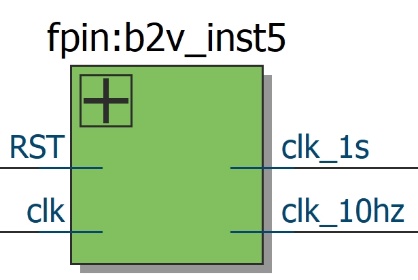
Figure 1. The schematic diagram of the frequency divider (Photo/Picture credit: Original).
2.2. Counter
The authors established a system consisting of two decimal counters to symbolize the units of seconds and minutes, two hex counters to symbolize the tens of seconds and minutes, and one twenty-four counter to symbolize the hours [6]. In this study, the researchers made the decision to utilize the LPM function of Verilog HDL for the implementation of the counters. This choice was made due to its capacity to minimize the amount of code required, hence decreasing the likelihood of errors during the coding phase and alleviating the burden of debugging in subsequent stages.
The schematic depicted in Figure 2 illustrates the structure of a decimal counter. While the decimal and hexadecimal counters share similarities, the 24-bit counter offers the advantage of eliminating the requirement to select a rounded output during the LPM production process. The term “clock” denotes the input that represents the passage of time [7]. The term “cout” is used to denote the output stream in programming. The abbreviation “sclr” is commonly used to denote the connection of the reset signal. The inclusion of a “LOAD” signal in the design facilitates manual time modification by allowing for the changing of the high and low values of seconds, minutes, and hours.
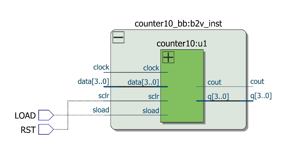
Figure 2. The schematic diagram of the a decimal counter (Photo/Picture credit: Original).
The flow of counter counting and bit feeding is depicted in Figure 3. The term “counter_6” denotes a counter that operates in the hexadecimal number system. The term “counter_10” denotes a decimal counter. The term “counter_24” denotes a counter with a bit width of 24 [8].
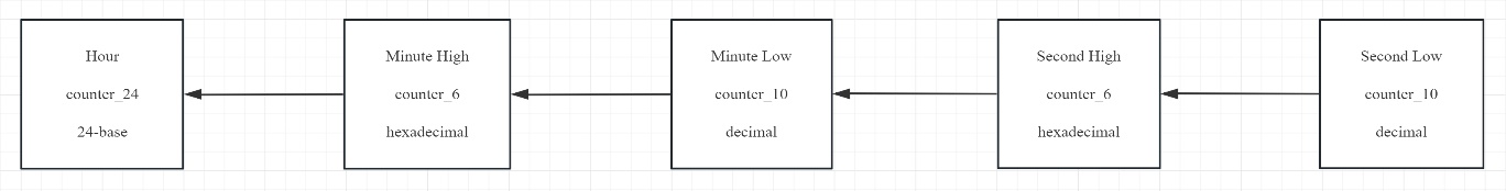
Figure 3. The flow of counting and feeding of the counter (Photo/Picture credit: Original).
2.3. Decoder
A decoder is a fundamental electronic circuit element employed to transform one or more input signals into equivalent output signals in the digital domain. The primary purpose of this device is to determine and activate specific output lines based on the input signal’s state, hence facilitating the implementation of various logic operations [9]. The decoder is employed in this design to transform the signals originating from the counter into output signals that are capable of being exhibited by the seven-segment digital tube.
The schematic diagram of the decoder is depicted in Figure 4, wherein the labels “led0” through “led3” correspond to the low second, high second, low minute, and low minute, respectively. The display visually creates a static display effect due to the dynamic scanning clock frequency being 10Hz, which is below the threshold frequency perceived by the human eye.
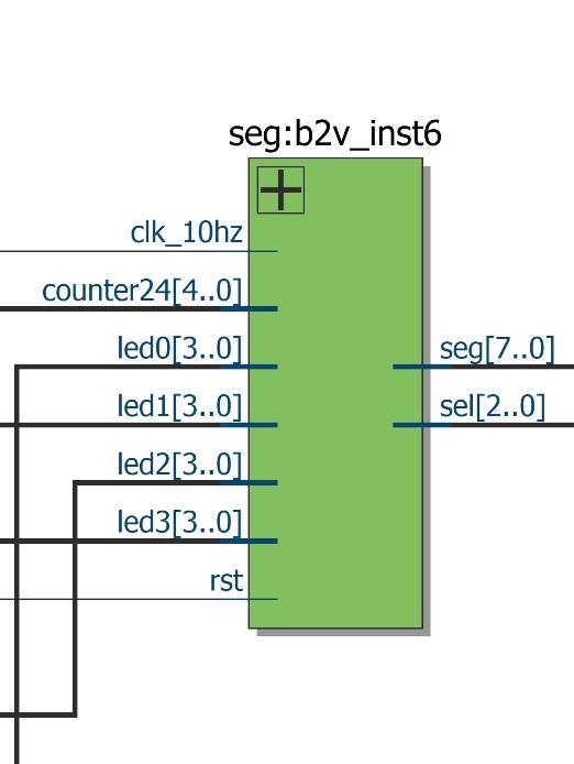
Figure 4. The schematic diagram of the a decoder (Photo/Picture credit: Original).
The notation “seg [7.0]” represents the output signal for an eight-bit segment code, while “sel [2.0]” represents the output signal for a three-bit slice code [10]. The purpose of segment code signal is to condense the state of the entire digital tube into a single byte, whereas slice code signal aims to encapsulate the state of each particular segment into multiple bits separately. Chip code signals are commonly employed in applications that necessitate advanced control due to their enhanced flexibility. Conversely, segment code signals are typically utilized for simpler digital display requirements, such as the digital clock incorporated in this particular design.
3. Comprehensive Circuit Design
In the process of composing the highest-level module, the authors produced module diagrams derived from the submodules. Subsequently, these module diagrams were interconnected to construct the top-level module, without resorting to instantiation statements for the purpose of implementing the design of said top-level module. The utilization of submodule diagrams for interconnection purposes offers a more streamlined and direct approach, hence facilitating the design process by eliminating the requirement for instantiation statements and detailed hardware descriptions. Furthermore, the reduction of errors in creating source code can be achieved through the process of designing and linking at the module diagram level. The diagram depicted in Figure 5 illustrates the circuit configuration subsequent to its establishment.
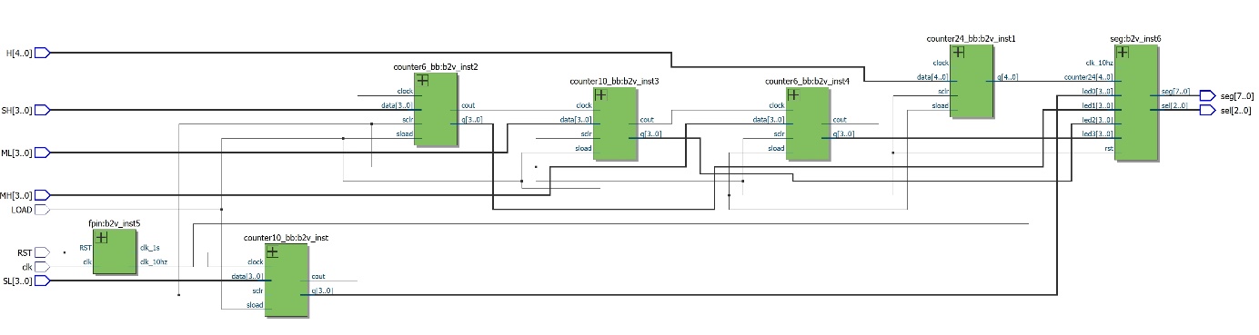 Figure 5. Connection of the completed circuit diagram (Photo/Picture credit: Original).
4. Analysis and Simulation Results
The simulation of the clock function is depicted in Figure 6. The image illustrates that when the minute count hits 59, it undergoes an automatic transition to 00. Simultaneously, the hour advances by one unit, transitioning from 13 to 14.
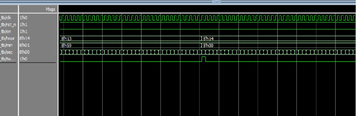
Figure 6. Clock function simulation diagram (Photo/Picture credit: Original).
The simulation diagram of the time setting function is depicted in Figure 7. When the time is manually adjusted, the counter is able to accurately update and exhibit the inputted time.
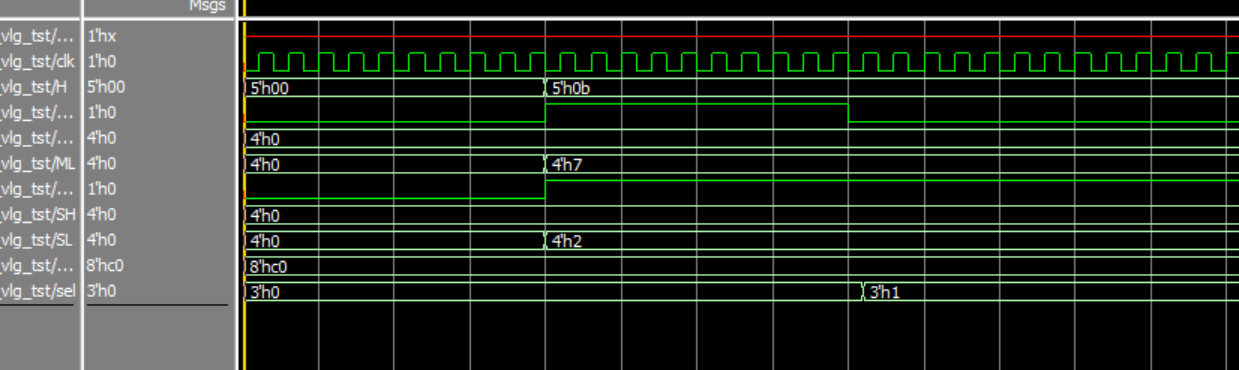
Figure 7. Manual adjustment function simulation diagram (Photo/Picture credit: Original).
5. Limitations and Future Directions
The process of creating a primary file from a network of interconnected subordinate files has certain benefits, but it also presents evident disadvantages and constraints. The design’s portability may be constrained as a consequence. The design implemented in this approach is constrained to a particular simulation tool, as shown by the module diagram level design approach. This implies that the design may exhibit suboptimal performance when deployed on diverse hardware platforms. Furthermore, this methodology presents challenges in managing intricate circuit designs. The process of connecting module diagrams for extensive and intricate digital designs is deemed too convoluted and ineffective. Moreover, this strategy imposes restrictions on the utilization of automated technologies. The process of hardware design frequently depends on the utilization of automated technologies, including synthesis tools, layout tools, and timing analysis tools. In order to function effectively, these tools necessitate precise hardware description language source code and do not derive sufficient information alone from the module diagram. In conclusion, while the utilization of module diagram design and connectivity leads to a reduction in code volume, the adoption of a hardware description language for the instantiation of submodules proves to be a superior option in terms of design portability and precision. The utilization of hardware description languages is attributed to their provision of enhanced tools and syntax, hence enabling the design to achieve a higher degree of precision and controllability.
The digital clock incorporated in this design alone possesses the fundamental capability of presenting the current time and allowing manual adjustments. However, this limited functionality may not be suitable for certain clock usage circumstances seen in everyday life. In the future, a potential avenue for improvement involves the incorporation of additional functionalities, such as a comprehensive time chime, alarm clock, timer, and other related features. Simultaneously, additional display modules can be incorporated to present supplementary information, such as the year, month, and day. In prospective developments, the integration of a toggle mechanism could be implemented to facilitate the transition between a 12-hour and 24-hour timer format. Additionally, the 12-hour timer can be enhanced with the inclusion of an AM and PM indicator on its display. By implementing these enhancements, the current design will be transformed into a digital clock with improved functionality.
6. Conclusion
This thesis provides an in-depth exploration into the design and realization of a digital clock developed in Verilog, augmented with a manual timing adjustment feature. Central to this design are three pivotal modules: the frequency divider, counter, and decoder. The culminating simulation confirmed the system’s precision and reliability.
To encapsulate, the research presented herein underscores Verilog’s prowess as a formidable and efficient tool for digital clock design endeavors. The synergistic blend of the frequency divider, counter, and decoder ensures the clock’s delivery of exact temporal representation, unwavering operation, and modifiable attributes. Verilog’s intrinsic flexibility and hardware description capabilities empower designers to refine and customize the digital clock for diverse scenarios, thereby aligning with users’ nuanced demands. This adaptability underscores the vital role of such digital tools in our modern landscape. To further elevate the digital clock’s utility and dynamism, future iterations could encompass additions like an hourly chime, an option to toggle between 12-hour and 24-hour formats, and an integrated temperature display. Such enhancements not only amplify the clock’s functional breadth but also ensure it remains attuned to evolving user needs and contemporary applications.
References
[1]. Li, W., Li, S., Zeng, Q., & Zhou, C. (2023). A Review of Design of Digital Clock Based on Verilog HDL. Highlights in Science, Engineering and Technology, 46, 289–297.
[2]. Zhongjian Gao, Maojin Wei, Ruige Zhang, & Lianzhou Rao. (2016). Design study of Verilog hdl digital clock circuit. Journal of Pingxiang University (3), 5.
[3]. Fan, H., Wang, S., Mao, N., & Dai, K. (2019). Development of Tibetan Multifunctional Digital Clock Based on FPGA. Journal of Physics: Conference Series, 1288(1), 012023.
[4]. Sau, S., Paul, R., Biswas, T., & Chakrabarti, A. (2012). A novel AES-256 implementation on FPGA using co-processor-based architecture. Proceedings of the International Conference on Advances in Computing, Communications, and Informatics - ICACCI ‘12.
[5]. Tian, W, & Xingzhong, X. (2018). Design of verilog-based encoder and decoder for scma system. Modern Electronics Technique.
[6]. Hao, L. (2008). Design of general frequency divider based on fpga using verilog hdl. Science Mosaic.
[7]. Ren Q, Liu Yi, & Wu Ji. (2015). Research on the advantages of parametric module library in Verilog design. Instrumentation Technology (7), 2.
[8]. McNamara, M. T. Y. IEEE Standard Verilog Hardware Description Language. The Institute of Electrical and Electronics Engineers (2001). IEEE Computer Society, Washington, DC, 1364-2001.
[9]. Tala, D. K. (2003). Verilog tutorial. WWW page. http://www. asic-world. com/verilog/veritut. html. (in English).
[10]. Palnitkar, S. (2003). Verilog HDL: A Guide to Digital Design and Synthesis (Bk/CD-ROM). Prentice-Hall, Inc.
Cite this article
Wang,Y. (2023). Verilog-based digital clock design methodology. Theoretical and Natural Science,14,102-107.
Data availability
The datasets used and/or analyzed during the current study will be available from the authors upon reasonable request.
Disclaimer/Publisher's Note
The statements, opinions and data contained in all publications are solely those of the individual author(s) and contributor(s) and not of EWA Publishing and/or the editor(s). EWA Publishing and/or the editor(s) disclaim responsibility for any injury to people or property resulting from any ideas, methods, instructions or products referred to in the content.
About volume
Volume title: Proceedings of the 3rd International Conference on Computing Innovation and Applied Physics
© 2024 by the author(s). Licensee EWA Publishing, Oxford, UK. This article is an open access article distributed under the terms and
conditions of the Creative Commons Attribution (CC BY) license. Authors who
publish this series agree to the following terms:
1. Authors retain copyright and grant the series right of first publication with the work simultaneously licensed under a Creative Commons
Attribution License that allows others to share the work with an acknowledgment of the work's authorship and initial publication in this
series.
2. Authors are able to enter into separate, additional contractual arrangements for the non-exclusive distribution of the series's published
version of the work (e.g., post it to an institutional repository or publish it in a book), with an acknowledgment of its initial
publication in this series.
3. Authors are permitted and encouraged to post their work online (e.g., in institutional repositories or on their website) prior to and
during the submission process, as it can lead to productive exchanges, as well as earlier and greater citation of published work (See
Open access policy for details).
References
[1]. Li, W., Li, S., Zeng, Q., & Zhou, C. (2023). A Review of Design of Digital Clock Based on Verilog HDL. Highlights in Science, Engineering and Technology, 46, 289–297.
[2]. Zhongjian Gao, Maojin Wei, Ruige Zhang, & Lianzhou Rao. (2016). Design study of Verilog hdl digital clock circuit. Journal of Pingxiang University (3), 5.
[3]. Fan, H., Wang, S., Mao, N., & Dai, K. (2019). Development of Tibetan Multifunctional Digital Clock Based on FPGA. Journal of Physics: Conference Series, 1288(1), 012023.
[4]. Sau, S., Paul, R., Biswas, T., & Chakrabarti, A. (2012). A novel AES-256 implementation on FPGA using co-processor-based architecture. Proceedings of the International Conference on Advances in Computing, Communications, and Informatics - ICACCI ‘12.
[5]. Tian, W, & Xingzhong, X. (2018). Design of verilog-based encoder and decoder for scma system. Modern Electronics Technique.
[6]. Hao, L. (2008). Design of general frequency divider based on fpga using verilog hdl. Science Mosaic.
[7]. Ren Q, Liu Yi, & Wu Ji. (2015). Research on the advantages of parametric module library in Verilog design. Instrumentation Technology (7), 2.
[8]. McNamara, M. T. Y. IEEE Standard Verilog Hardware Description Language. The Institute of Electrical and Electronics Engineers (2001). IEEE Computer Society, Washington, DC, 1364-2001.
[9]. Tala, D. K. (2003). Verilog tutorial. WWW page. http://www. asic-world. com/verilog/veritut. html. (in English).
[10]. Palnitkar, S. (2003). Verilog HDL: A Guide to Digital Design and Synthesis (Bk/CD-ROM). Prentice-Hall, Inc.