


1. Introduction
Various types of heart diseases have become one of the leading causes of death annually, with the death toll exceeding one million each year [1]. Specialized cells in the heart generate electrical impulses, which spread through the atria and ventricles of the heart, causing the heart to contract and pump blood. The tiny changes in electric currents generated by these impulses, which are the source of the Electrocardiogram (ECG) signal, can be detected through the skin by the electrode. After detecting and analyzing the ECG curve, doctors can evaluate one’s heart condition. But one of the main problems is that heart disease often happens suddenly, and the accurate but huge devices in hospitals can’t be used to detect ECG signals in time. Wearable ECG signal-detecting devices have become an emerging technology to deal with the sticky situation [2-4]. Those wearable devices can detect the patients’ ECG curves and store them so that doctors can do treatments when the patients reach to hospital later [5].
However, the ECG signal only has an amplitude of several microvolts and usually has a lower frequency of about 0.5 Hz. Therefore, flicker noise becomes a big problem [6-8]. In addition, some unexpected signals need to be filtered, such as the 50 Hz/60 Hz interference caused by the country’s power lines or other bioelectrical interferences [9]. Therefore, a highly integrated analog front-end (AFE) circuit is necessary. AFE circuit can amplify the weak ECG signal and meanwhile suppress the interference ability of the acquired signal [10]. The amplifier circuit is a significant part of the analog front-end circuit. Low noise amplifier (LNA) is extensively used in AFE circuits on account of its ability to produce lower noise.
There are many researches about the amplifier circuit for wearable ECG devices. Wei proposed a preamplifier circuit that can weaken the electrode imbalance interference [11]. The authors provided an amplifier that has a higher cut-off frequency of 0.52 Hz and a lower cut-off frequency of 108. 6 Hz. And the input-referred noise was 3.5 \( μ{ V_{RMS}} \) . In the study of Chen [12], an amplifier circuit with a bandwidth of 250 Hz, a gain from 51dB to 96 dB, an input-referred noise of 6.52 \( μ {V_{RMS}} \) and a CMRR of 226 dB was designed.
However, the amplifiers in the research can’t achieve low noise, low power and a higher bandwidth at the same time. A wider bandwidth can provide higher resolution, thereby obtaining more accurate ECG signals. More detected signals allow doctors to identify potential heart problems more accurately. Higher frequency bandwidth can capture important information in ECG signals that might be lost. The information may include abnormal signals that cannot be detected at lower frequencies. An amplification circuit with a wider bandwidth can reduce signal distortion caused by filters, thus improving the quality of ECG signals. In some applications that require quick response, higher bandwidth can provide faster signal processing speed.
Nevertheless, the power consumption should be lower enough so that the wearable device can work longer. The total noise of the circuit should be lower to make the waveform clearer. Typically, reducing circuit noise requires increasing the current or power consumption, and reducing power consumption often leads to increased noise. Making the balance between power and noise is a significant challenge.
In this paper, an improved low-noise amplifier circuit has been proposed. The circuit is based on a conventional instrumentation amplifier and consists of two stages. The op-amps were replaced with an Operational Transconductance Amplifier (OTA) and the Berkeley Short-channel Insulated-gate field-effect transistor (BSIM) 180 nm CMOS model is used in the OTA. The circuit also has a Driven-Right-Leg (DRL) circuit part, which can tremendously reduce the effect of common-mode noise. The most essential and innovative improvement is that the circuit has a higher bandwidth.
2. Methodology
2.1. Design criteria
Typically, the frequency range of common ECG signals is from 0.05 Hz to 150 Hz. However, most ECG machines are designed with a higher bandwidth to capture and display high-frequency details that may be clinically important. In practice, a bandwidth of 0.05 to 250 Hz is often used. A higher bandwidth ensures the signal integrity of the faster components of the ECG, such as the QRS complex, which has a higher frequency content. Bandwidth up to 250 Hz also helps in noise reduction, as it eliminates frequencies that are out of this range, which is most likely to be due to muscle artifacts, power line interferences, or other electronic interferences.
The amplified ECG signals are usually fed into an analog-to-digital converter (ADC) for further processing and display. Most ADCs require inputs in certain voltage ranges (often around 0 to 5 V or -10 to +10 V). A gain of 40 dB can help to bring the small ECG signals into the appropriate range for the ADC. In addition, a gain of 40 dB is often a good compromise that allows for sufficient amplification without risk of saturation.
The ECG signals being measured are very small, often in the range of microvolts. By keeping the noise level low, the accuracy of the ECG signal is maintained. High noise levels may obscure clinically relevant information or lead to misinterpretation of the ECG signal. This could potentially lead to incorrect diagnoses.
Keeping the noise level low improves the signal-to-noise ratio (SNR), which in turn improves the quality of the signal. The power consumption should also be as low as possible to increase battery life.
High capacitance could lead to signal distortion and phase shifts in the ECG signal, which might decrease the accuracy of the ECG curve. High-value capacitors take longer to charge and discharge, which can slow down the circuit response time. This could be problematic in time-critical applications such as ECG signal amplification. Therefore, it is generally recommended to use capacitors with a value lower than 1nF in ECG signal amplifier circuits to avoid these potential issues and ensure accurate, reliable ECG readings.
According to the actual requirement of ECG amplifiers and wearable devices. The amplifier circuit in the design must, at minimum, meet the following specifications:
- Frequency range: 0.1 Hz – 250 Hz ± 10%
- Differential mode gain: 40 dB ± 5 dB
- Total integrated input-referred noise: <4 \( μ {V_{RMS}} \)
- Total power consumption: <5µ W
- Total employed capacitance: < 1n F
2.2. Conventional 3- operational-amplifier Instrumentation Amplifier Circuit
A conventional 3-Operational-Amplifier (Op-Amp) instrumentation amplifier circuit is a type of difference amplifier that amplifies the difference between the voltages at its two input terminals. The circuit can be seen in Figure 1. Rather than the one op-amp design, a three op-amp design is used to provide high input impedance, making it suitable to measure small signals among common mode signals.
The first two op-amps form a differential amplifier stage that amplifies the differential voltage between two input ends. The third op-amp is a difference amplifier that subtracts the output of one input amplifier from the other to provide the final output.
However, there are limitations to this conventional 3-Op-Amp Instrumentation Amplifier Circuit. The cascaded nature of this design can limit the bandwidth of the amplifier. This is because an op-amp’s bandwidth decreases as the gain increases, which can affect the amplifier’s performance at high frequencies. Ideally R3 is equal to R3’ and R4 is equal to R4’. But actually, the resistors that the factory produced always have a at least 1% mismatch. The output gain can be affected by mismatches in the resistors used in the circuit, and by the op-amp’s offset voltage and bias current.
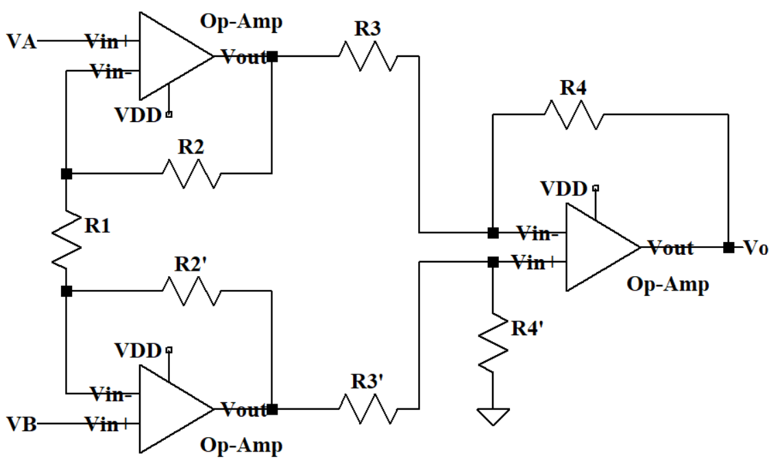
Figure 1. Schematic of the Conventional 3-Op-Amp Instrumentation Amplifier Circuit.
2.3. The modified circuit
The overall modified circuit can be seen in Figure 2 and it mainly consists of two parts. The first part is a two-stage amplifier circuit. The second part is the DRL circuit. VRA is connected to one’s right arm through electrodes while VLA will be connected to the left arm. VRL is connected to one’s right leg. There are four OTAs in the circuit and the supply voltage of every OTA is set to be 1.6 V. The input bias voltage Vref, which is half of the VDD, is used to keep the OTA’s output at a mid-level in the absence of an input signal. The bias voltage can allow the OTA to have the maximum output swing and prevent it from distortion.
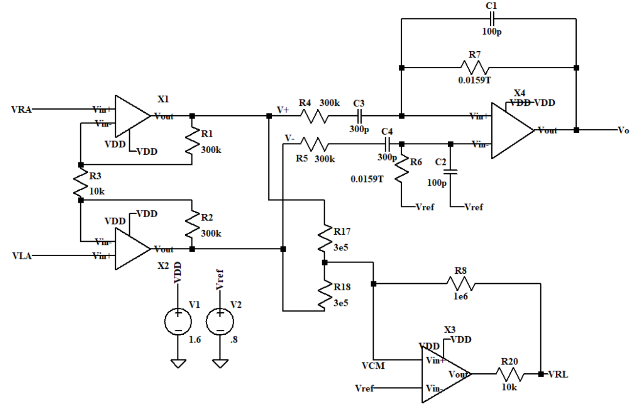
Figure 2. Schematic of the modified circuit.
2.4. First stage: Differential input and output buffer
The first stage circuit which can be seen in Figure 3 is a differential input and output buffer. It can collect the differential voltage of the weak ECG signal and make it stronger. Then the differential output can pass the differential mode signal V+ and V- to the second stage. The circuit has R1 and R2 as negative feedbacks. The theoretical differential gain of the first stage is equal to 35.71 dB.
\( {A_{vd1}}=\frac{{R_{1}}+{R_{2}}+{R_{3}}}{{R_{3}}}\ \ \ (1) \)
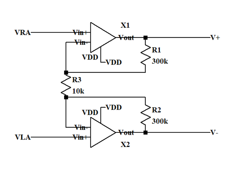
Figure 3. Schematic of the first stage circuit.
2.5. Second stage: Differential-to-single ended amplifier
The second stage which can be seen in Figure 4 is a differential-input to the single-output amplifier. The bias resistor R6 and capacitor C2 can reduce the impact of the OTA’s input current on its performance. Considering R7 is big enough, the theoretical differential gain of the second stage is 9.54 dB.
\( \frac{{{A_{vd2}}=C_{3}}}{{C_{1}}}\ \ \ (2) \)
So, the total ideal differential gain is 45.25 dB.
\( {A_{vd}}={A_{vd1}}+{A_{vd2}}\ \ \ (3) \)
C1 and R7 work as a RC parallel positive feedback and the lower cut-off frequency is 100m Hz.
\( {f_{low}}=\frac{1}{2π{R_{7}}{C_{1}}}\ \ \ (4) \)
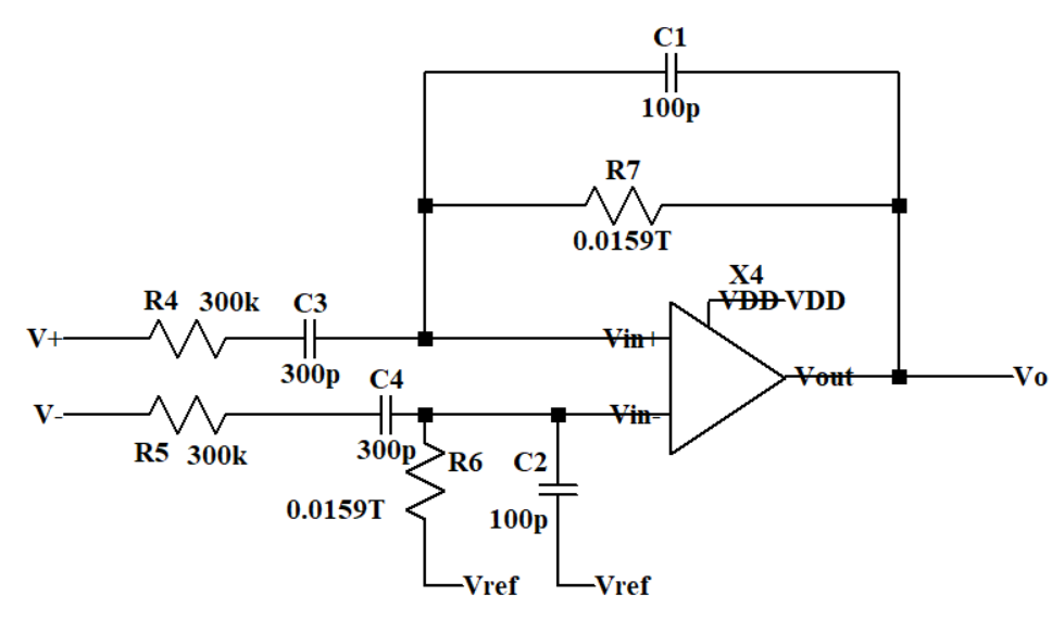
Figure 4. Schematic of the second stage circuit.
2.6. Driven-right-leg circuit
The human body has different electromagnetic interference in different environments, such as 50/60Hz electromagnetic interference generated by power lines and electrical equipment. This interference is conducted into the ECG amplification circuit through the human body, forming common-mode noise. Common-mode noise has a serious impact on the measurement of ECG signals, masking the real ECG signal. The DRL circuit in Figure 5 can minimize the common-mode noise. R17 and R18 are large resistors to collect common mode signals. Then an OTA with positive feedback can amplify the common-mode noise signal in the reverse phase and input it into the human body through the right leg, thereby canceling the common-mode noise in the circuit.
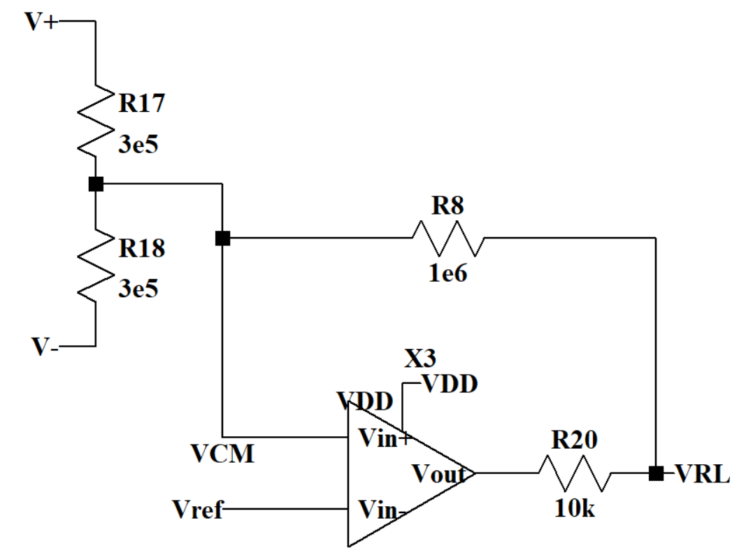
Figure 5. Driven-Right-Leg circuit.
2.7. Design of the OTA circuit
OTA is a type of amplifier whose differential input voltage produces an output current, which is in contrast to the Op-Amp. The gain of the OTA can be adjusted by changing the bias current, making it a useful component in applications where gain control is necessary.
This circuit structure of OTA X1 and X2 can be seen in Figure 6. This operational amplifier incorporates MILLER compensation. I1 functions as an external current source that provides biasing, and M5 serves as a backside current source giving DC bias for the transconductance transistor. M1 and M2 are configured as differential-input stages. C1 is deployed to isolate the primary pole from the sub-dominant one. The zero point, positioned initially in the right half-plane, can be translocated to the left half-plane to bolster the stability of the phase margin. The higher cut-off frequency is inversely proportional to the value of C1.
According to the structure of OTA X3 and X4 in Figure 7 and Figure 8, the current goes through PMOS M3 and M4 contributes most of the 1/f noise. 1/f noise gets higher when the current gets higher but the power will meanwhile get higher. Another consideration is that if the current flows through the OTA is too large or too small, the amplifier may not work in saturation region. After making the trade-off, the value of the current source and the W/L ratio of M5 and M7 have been changed to balance the noise and power. The value of the current sources in OTA X3 and X4 were set to be 8n A. Therefore, the OTAs all work in subthreshold region, which has lower power consumption than above-threshold region. Transistors in the subthreshold region generate less heat, which helps to reduce the operating temperature and improve the reliability and lifespan of the device.
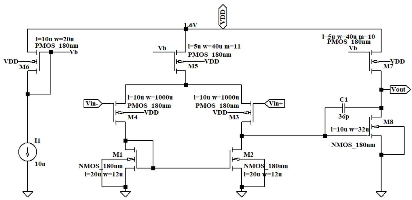
Figure 6. The circuit of OTA X1 and X2.
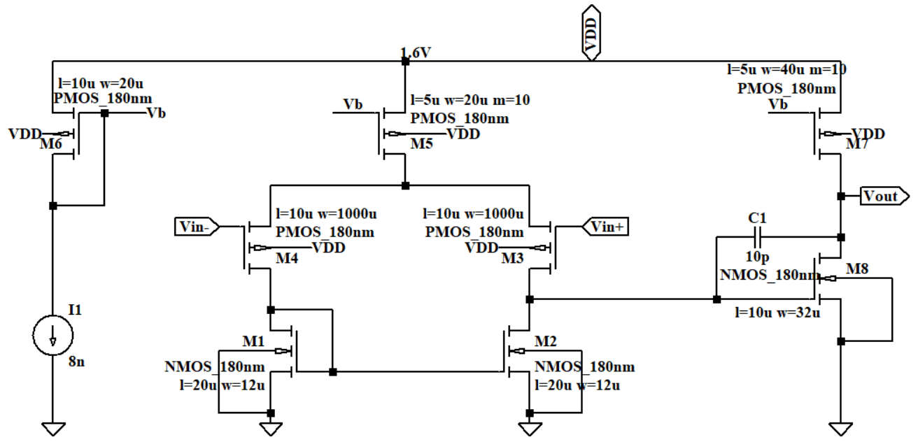
Figure 7. The circuit of OTA X3.
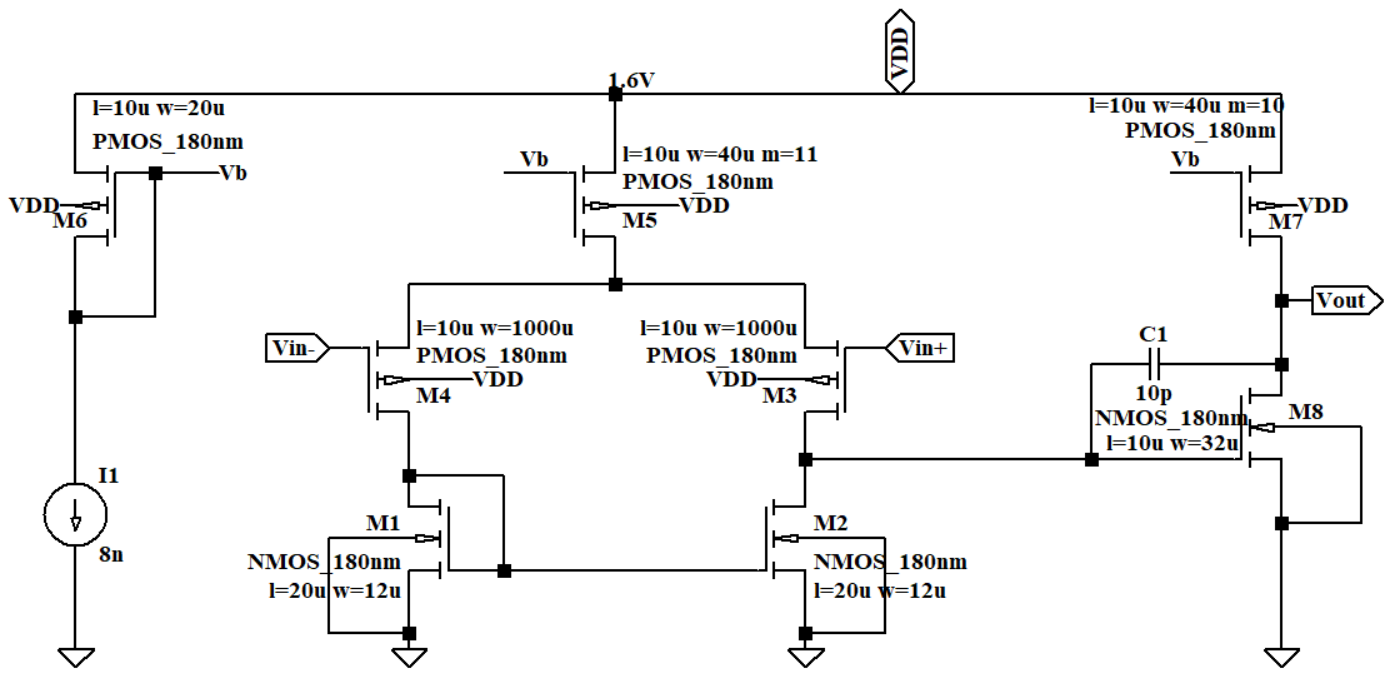
Figure 8. The circuit of OTA X4.
3. Results and discussions
3.1. Simulation based on LTspice
LTspice is a high-performance SPICE simulator software that enhances the design of analog and mixed electronic devices and circuits. The reason why LTspice is used for the simulation is that it can model actual performance parameters of components such as the BSIM 180nm CMOS model used in the circuit.
3.2. Simulated human body
For further simulation, the circuit in Figure 9 can work as the real human body. V1 works as the ECG signal and has an AC value of 0.1 μV. I1 can simulate the power-line interference and it has a 50 Hz sine signal output. R5, R6 and R7 are the body resistance. Electrodes can translate bio-signals into electrical ones, and these are subsequently channeled toward the electric component of the recording system. The electrode model used for simulation is a 2kΩ resistor in series with a 1 MΩ resistor and a 50 nF capacitor.
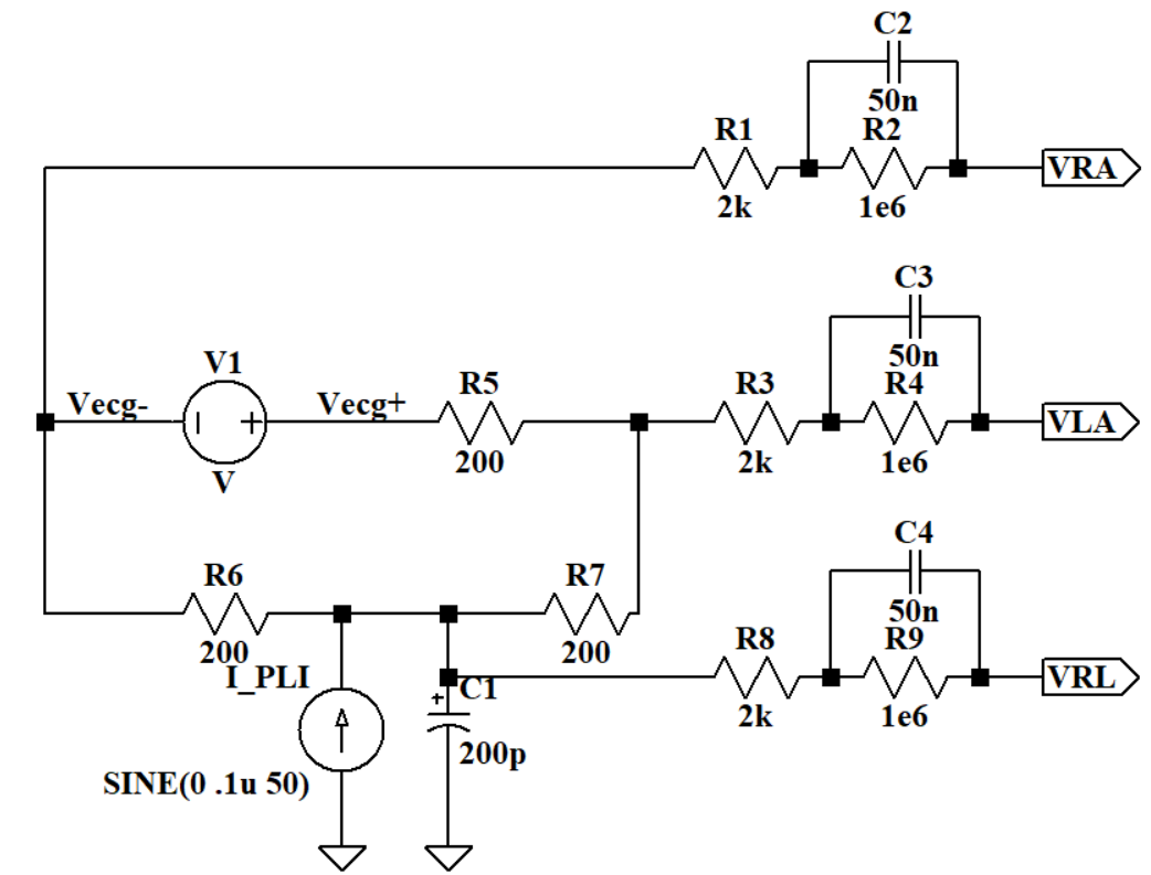
Figure 9. Human body simulation circuit.
3.3. Overall gain and bandwidth analysis
As for the simulation, the differential gain between VRA and VLA is about -3.5 dB, which means before getting into the amplifier circuit, there has already been a 3.5 dB loss. When doing measurements, there is no need to access the human body, so the 3.5 dB lost does not need to be taken into account.
According to the differential gain curve in Figure 10, the lower cut-off frequency is about 101m Hz and the higher cut-off frequency is 252 Hz, so the bandwidth is 251. 9 Hz. The mid-band gain is t 43.98 dB.
The CMRR calculated in this article is not the real CMRR but describes how much the DRL circuit affects the common mode gain. Firstly, Vecg was set to be zero. Then VRL was connected to VCM and a 0.1μ AC was added in the current source. After that R4 and R5 were made to have a 1% mismatch. Then measure \( {V_{o}} \) at 50 Hz when the DRL circuit was connected and measured VRA when VRL was connected to Vref. As a calculation, the common mode gain is -94 dB.
\( {A_{CM}}=\frac{{V_{o}}}{{V_{RA}}}\ \ \ (5) \)
Recalling from earlier simulation that \( {A_{od}} \) is 43.98 dB. Therefore, CMRR is 137.98 dB, which means the DRL circuit could reduce the common mode gain and enhance the amplifier’s ability to amplify differential mode signals.
\( CMRR=\frac{{A_{od}}}{{A_{CM}}}\ \ \ (6) \)
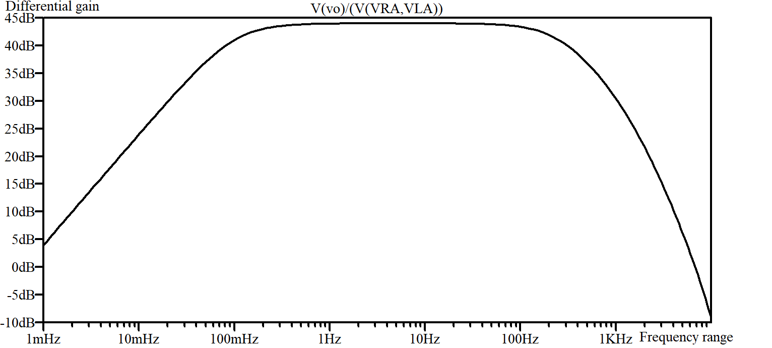
Figure 10. Differential gain curve.
3.4. Noise analysis
The feedback resistors and OTA contribute to the input-referred noise of the LNA. However, because of the low bandwidth, the noise from the feedback resistor can be ignored. Therefore, the overall noise of the LNA is primarily owing to the OTA.
As a simulation result, the differential gain is 43.98 dB and the total RMS noise is 586.6 \( μ V \) .So the total integrated input-referred noise is 3.70 \( μ {V_{RMS}} \) .That means the circuit has a very low signal-to-noise ratio, which can enhance the signal quality.
\( total integrated input-referred noise=\frac{total RMS noise}{{A_{od}}}\ \ \ (7) \)
According to the formula of Noise Efficiency Factor (NEF) first supposed in [13].
\( NEF={V_{n,in,RMS}}{(\frac{2{I_{tot}}}{{φ_{t}}·4KT·BW·π})^{\frac{1}{2}}}\ \ \ (8) \)
\( {I_{tot}} \) is the total current being used in the whole design, so it would be all of the current coming out of the VDD supply. \( {φ_{t}} \) is 1.5 mV and BW is 251. 9 Hz. K is Boltzmann’s constant and T is Kelvin temperature. NEF primarily measures the relationship between the circuit’s noise performance and power consumption. The lower the NEF, the less noise the circuit generates at the same power consumption. The lower the NEF, the lower the power consumption of the circuit while maintaining the same noise performance. As a calculation result, the NEF of this circuit is 14.38, which means that the power and noise efficiency haven’t met the perfect trade-off. However, a 14.38 NEF is still an acceptable parameter.
3.5. Total power consumption
Theoretically, the total current is the current flows through every component and it is calculated to be 2.52 \( μ A \) .The simulation result shows that the total current is 2.479 \( μ A \) .
\( {P_{tot}}={I_{tot}}·VDD\ \ \ (9) \)
The theoretical power consumption is \( 4.032 μW \) and the simulation result was 3.96 \( μW \) .
3.6. Summary and Comparison
In summary, the designed circuit has a higher bandwidth of about 251. 9 Hz. Meanwhile, it has a high CMRR of about 138 dB, a total integrated input-referred noise of \( 3.70μ {V_{RMS}} \) and a total power consumption of about 3.96 \( μ W \) .Compared with the existed research, the circuit proposed in the paper has a low noise, low power consumption and a perfect high bandwidth at the same time. The improved circuit meets the design criteria well. It has absorbed existing research’s advantages and eliminated drawbacks. Table 1 shows the comparisons between the results in this paper and in existed essays.
Table 1. Comparisons between the result in this paper and existed essays.
Wei, 2020 [11] | Chen Y et al, 2014 [12] | The circuit proposed in this paper | |
Frequency range | 0.52 Hz-108.6 Hz | 250 Hz | 101m Hz-252 Hz |
Supply voltage | 1.8 V | 0.6 V | 1.6 V |
Differential gain | 47.6 dB-59.8 dB | 51-96 dB | 43.98 dB |
Total integrated input-referred noise | 3.50 \( μ {V_{RMS}} \) | 6.52 \( μ {V_{RMS}} \) | 3.70 \( μ{ V_{RMS}} \) |
Power consumption | 70 \( μ W \) | NA | 3.96 \( μ W \) |
4. Discussions
A high enough bandwidth is the key focused index in the design. So, the capacitors in the OTA of the first stage were changed to control the lower cut-off frequency and used RC parallel feedback to set a higher cut-off frequency. However, a higher bandwidth means that some unexpected signal in other frequencies would also be amplified, which contributed to higher input-referred noise. Furthermore, the power consumption also needed to get lower to make the wearable device work longer. Based on a conventional 3-op-amp Instrumentation amplifier, a two-stage amplifier circuit with three OTAs was designed and a DRL circuit that can decrease common mode noise was added.
After finishing the circuit design, the circuit was simulated based on LTspice. Simulation results showed that the circuit has high bandwidth, low noise, and power consumption. The result is approximately equal to the theoretical calculation.
However, reducing the size of the circuit has been our main problem. The two 0.0159T Ω resistors used in the feedback and bias circuit might be too large to be integrated into small chips. For the future iteration, the large resistors can be replaced with a pseudo resistor, which consists of CMOS and is easier to integrate.
5. Conclusion
With the swift advancement of technology, medical wearable devices are raising the awareness of millions of people. Keenly aware of the high ratio of heart disease and the significance of monitoring heart beats at any time, a low-power low-noise ECG signal amplifier circuit that is suitable for wearable devices has been proposed in this paper. The two-stage structure can provide stable differential gain and the DRL circuit can significantly reduce common mode noise and increase CMRR. The OTA contributes lower noise and the RC paralleled feedback accurately controls the cut-off frequency. Compared with amplifier circuits in existing research, our improved amplifier circuit has a higher bandwidth of 252 Hz and also successfully has a low power consumption and noise. In addition, instead of using 12-18 leads medical-grade ECG detecting equipment in the hospital, our circuit only needs 3 leads and therefore it is wearable. Because of the low power consumption, low noise, and stable gain, the wearable device can record patients’ ECG curve constantly and provide a high-accuracy ECG curve for doctors to do further treatments. Wearable devices characterized by reduced power consumption and diminished noise levels are progressively emerging as a trend. It is full of expectations that the research will more or less promote the update and iteration of wearable ECG detection devices. In this way, the practicality and durability of wearable devices can be better developed.
References
[1]. Sufi F, Fang Q, Khalil I and Mahmoud S 2009 Novel methods of faster cardiovascular diagnosis in wireless telecardiology IEEE J. Sel. Areas Commun. 27 537
[2]. Winokur E, Delano M and Sodini C 2013 A wearable cardiac monitor for long-term data acquisition and analysis IEEE Trans. Biomed. Eng. 60 189
[3]. Wang N, Zhou J, Dai G, Huang J and Xie Y 2019 Energy-efficient intelligent ECG monitoring for wearable devices IEEE Trans. Biomed. Circuits Syst. 13 1112
[4]. Yin S, Li G, Luo Y, Yang S, Tain H and Lin L 2020 A single-channel amplifier for simultaneously monitoring impedance respiration signal and ECG signal Circuits Syst. Signal Process. 40 559
[5]. Ha S, Kim C, Chi Y, Akinin A, Maier C, Ueno A and Cauwenberghs G 2014 Integrated circuits and electrode interfaces for noninvasive physiological monitoring IEEE Trans. Biomed. Eng. 61 1522
[6]. Mazur A, Wang L, Anderson M, Yee R, Theres H, Pearson A, Olson W and Wathen M 2001 Functional similarity between electrograms recorded from an implantable cardioverter defibrillator emulator and the surface electrocardiogram Pacing Clin. Electrophysiol. 24 34
[7]. Black B, Stromberg K, Balen G, Ghanem R, Breedveld R and Tieleman R 2010 Is surface ECG a useful surrogate for subcutaneous ECG? Pacing Clin. Electrophysiol. 33 135
[8]. Himmrich E, Zellerhoff C, Nebeling D, Rosocha S, Przibille O, Nowak B and Liebrich A 2000 An welcher Stelle soll ein implantierbarer EKG-Event-Recorder plaziert werden? Zeitschrift für Kardiologie 89 289
[9]. David P and Michael N 2004 Design and Development of Medical Electronic Instrumentation:A Practical Perspective of the Design, Construction, and Test of Medical Devices John Wiley & Sons Inc 65
[10]. Zhang Y, Wang J, Xiong D and Guo L 2021 Design of wearable wireless bioelectric feedback control system Transducer Microsyst. Technol. 40 73
[11]. Wei C 2020 Analog front-end circuit design for ECG signal acquisition Anhui University doi: 10.26917/d.cnki.ganhu.2020.001280
[12]. Chen Y et al 2015 An Injectable 64 nW ECG Mixed-Signal SoC in 65 nm for Arrhythmia Monitoring IEEE J. Solid-State Circuits 50 375
[13]. Steyaert M and Sansen W 1987 A micropower low-noise monolithic instrumentation amplifier for medical purposes IEEE J. Solid-State Circuits 22 1163
Cite this article
Liu,X. (2023). Design of a high bandwidth ECG signal low noise amplifier circuit for wearable devices. Theoretical and Natural Science,25,12-22.
Data availability
The datasets used and/or analyzed during the current study will be available from the authors upon reasonable request.
Disclaimer/Publisher's Note
The statements, opinions and data contained in all publications are solely those of the individual author(s) and contributor(s) and not of EWA Publishing and/or the editor(s). EWA Publishing and/or the editor(s) disclaim responsibility for any injury to people or property resulting from any ideas, methods, instructions or products referred to in the content.
About volume
Volume title: Proceedings of the 3rd International Conference on Computing Innovation and Applied Physics
© 2024 by the author(s). Licensee EWA Publishing, Oxford, UK. This article is an open access article distributed under the terms and
conditions of the Creative Commons Attribution (CC BY) license. Authors who
publish this series agree to the following terms:
1. Authors retain copyright and grant the series right of first publication with the work simultaneously licensed under a Creative Commons
Attribution License that allows others to share the work with an acknowledgment of the work's authorship and initial publication in this
series.
2. Authors are able to enter into separate, additional contractual arrangements for the non-exclusive distribution of the series's published
version of the work (e.g., post it to an institutional repository or publish it in a book), with an acknowledgment of its initial
publication in this series.
3. Authors are permitted and encouraged to post their work online (e.g., in institutional repositories or on their website) prior to and
during the submission process, as it can lead to productive exchanges, as well as earlier and greater citation of published work (See
Open access policy for details).
References
[1]. Sufi F, Fang Q, Khalil I and Mahmoud S 2009 Novel methods of faster cardiovascular diagnosis in wireless telecardiology IEEE J. Sel. Areas Commun. 27 537
[2]. Winokur E, Delano M and Sodini C 2013 A wearable cardiac monitor for long-term data acquisition and analysis IEEE Trans. Biomed. Eng. 60 189
[3]. Wang N, Zhou J, Dai G, Huang J and Xie Y 2019 Energy-efficient intelligent ECG monitoring for wearable devices IEEE Trans. Biomed. Circuits Syst. 13 1112
[4]. Yin S, Li G, Luo Y, Yang S, Tain H and Lin L 2020 A single-channel amplifier for simultaneously monitoring impedance respiration signal and ECG signal Circuits Syst. Signal Process. 40 559
[5]. Ha S, Kim C, Chi Y, Akinin A, Maier C, Ueno A and Cauwenberghs G 2014 Integrated circuits and electrode interfaces for noninvasive physiological monitoring IEEE Trans. Biomed. Eng. 61 1522
[6]. Mazur A, Wang L, Anderson M, Yee R, Theres H, Pearson A, Olson W and Wathen M 2001 Functional similarity between electrograms recorded from an implantable cardioverter defibrillator emulator and the surface electrocardiogram Pacing Clin. Electrophysiol. 24 34
[7]. Black B, Stromberg K, Balen G, Ghanem R, Breedveld R and Tieleman R 2010 Is surface ECG a useful surrogate for subcutaneous ECG? Pacing Clin. Electrophysiol. 33 135
[8]. Himmrich E, Zellerhoff C, Nebeling D, Rosocha S, Przibille O, Nowak B and Liebrich A 2000 An welcher Stelle soll ein implantierbarer EKG-Event-Recorder plaziert werden? Zeitschrift für Kardiologie 89 289
[9]. David P and Michael N 2004 Design and Development of Medical Electronic Instrumentation:A Practical Perspective of the Design, Construction, and Test of Medical Devices John Wiley & Sons Inc 65
[10]. Zhang Y, Wang J, Xiong D and Guo L 2021 Design of wearable wireless bioelectric feedback control system Transducer Microsyst. Technol. 40 73
[11]. Wei C 2020 Analog front-end circuit design for ECG signal acquisition Anhui University doi: 10.26917/d.cnki.ganhu.2020.001280
[12]. Chen Y et al 2015 An Injectable 64 nW ECG Mixed-Signal SoC in 65 nm for Arrhythmia Monitoring IEEE J. Solid-State Circuits 50 375
[13]. Steyaert M and Sansen W 1987 A micropower low-noise monolithic instrumentation amplifier for medical purposes IEEE J. Solid-State Circuits 22 1163