


1. Introduction
As science and technology keep developing in this century, people start to realize the importance of maintaining good physical condition. Working out regularly, having a healthy diet, and visiting doctors are all approaches that people take to maintain a healthy physical state. However, visiting doctors and doing medical examinations are tedious, as they often take time and money. Therefore, wearable devices that can provide instant feedback become extremely popular, as they are more convenient and much cheaper than visiting doctors. Wearable devices were first used in 1956, as they were used to monitor the oxygen level in the blood during surgery [1]. Now, there are varieties of wearable devices in the market that have distinct functions, such as rings that can track sleep patterns, bracelets that can measure walking speed, and necklaces that can record heart conditions [2]. However, not all wearable devices can provide useful information that is meaningful to people, and not all of them are comfortable to wear. For example, one of the main reasons that people are resisting implantable glucose sensors is because they are invasive and uncomfortable to wear [3]. Some other devices, such as the Apple Watch developed by Apple, can only be used for eighteen hours before a recharge, which is extremely inconvenient.
Design the electrocardiogram (ECG) devices that are not invasive and have long-lasting batteries, it is required to use microcircuits that have very small power consumption. In this case, this circuit will have a small current and a small voltage level. As a result, a very small noise level will ultimately make a significant difference to the whole system, disrupting the heartbeat signal and distorting the morphological features of the ECG [4]. Therefore, one of the major issues for designing the circuit will be lowering the noise level while keeping both the current and the voltage low, to help the patient receive the most accurate diagnosis.
2. Methodology
2.1. The model of the traditional physiological monitoring circuit design method
Presently, there are numerous technologies regarding monitoring human body conditions. However, a large portion of those devices is invasive and tedious, which makes them hard to integrate into people’s daily lives. For example, Electroencephalogram (EEG), which can monitor live brain function, requires a huge device to be connected to the human brain skin [5]. Other devices such as smart watches can count the number of daily steps. However, this information is not quite useful, as the number of steps per day does not reflect a person’s physical health condition [6]. Therefore, people need new devices that are small and non-invasive so that they can be incorporated perfectly into people’s daily lives. Moreover, they have to be able to provide useful feedback information that can be used to analyze people’s physical health conditions. Lastly, these devices should be designed with long-lasting batteries and small power consumptions to minimize recharging [7].
The physical attributes of microcircuits determine that they have to be low-power, low-voltage, and low-current. Therefore, for signal-processing purposes, an applicable amplification circuit is required.
2.2. Improved amplification circuit design using LTspice
To design and simulate the circuit, the author uses LTspice software to assist. During the designing of the ECG circuit, since the specifications of this circuit make small noise very significant. Therefore, to minimize the common-mode pickup noise, the driven-right-leg (DRL) circuit is introduced [8]. Another benefit of adopting this circuit is that it is a safe way to ground the body. For instance, in cases where there is a sudden increase in the body’s voltage level, the operational amplifier enters a saturated state, essentially disconnecting the body from the circuit’s ground.
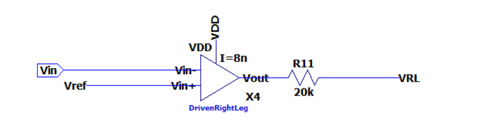
Figure 1. The DRL circuit.
As Figure 1. shows, the resistor, R11, set with a huge number, can protect the human body from suddenly raised current. Inside the op-amp, a capacitor can be placed between the op-amp’s input and output to compensate for the phase and adjust the bandwidth. To reduce the noise, this circuit can extract the common-mode signal through the reverse amplifier and then impose it on the human body [9].
To calculate the feedback of this part of the circuit, it is helpful to check Figure 2 below.
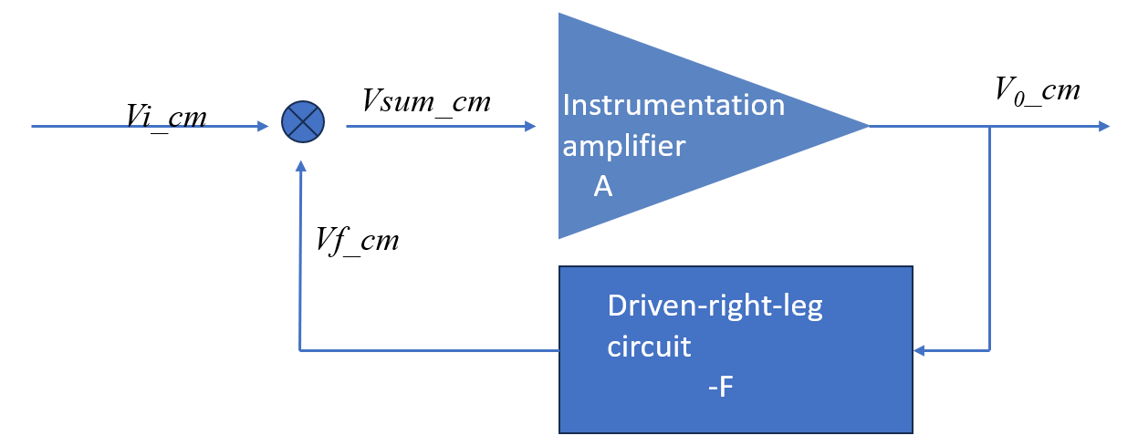
Figure 2. Demonstration of the feedback.
Based on Figure 2, one can easily calculate the relationship between the input and the output:
\( {V_{{0_{cm}}}}={V_{su{m_{cm}}}}×A\ \ \ (1) \)
\( {V_{su{m_{cm}}}}={V_{{i_{cm}}}}+{V_{fcm}}\ \ \ (2) \)
\( {V_{{f_{cm}}}}= -F×{V_{{0_{cm}}}}\ \ \ (3) \)
Therefore, the relationship can be deducted:
\( {V_{{o_{cm}}}}=\frac{{V_{{i_{cm}}}}}{1+F}\ \ \ (4) \)
After introducing the DRL circuit, the human-body model and the electrode model are designed to simulate real-life situations where the ECG device is connected to a human body with several electrodes, as shown in the Figure 3.
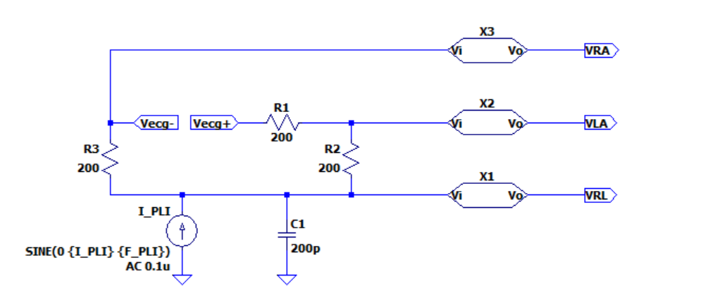
Figure3. The human body circuit.
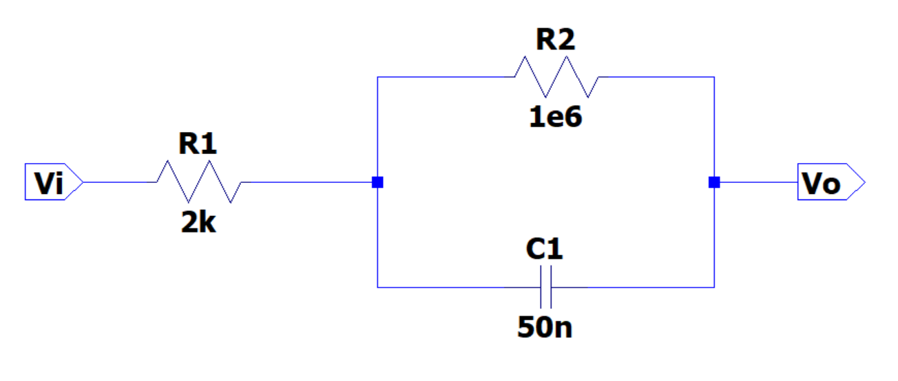
Figure 4. The electrode circuit.
Since the electrode is in contact with the human skin directly without any intermediate medium, the discomfort of the person wearing the electrode can be minimized. However, this design also raises the level of danger. Therefore, the electrode circuit is implanted with a very large contact impedance as shown in Figure 4 to ensure safety.
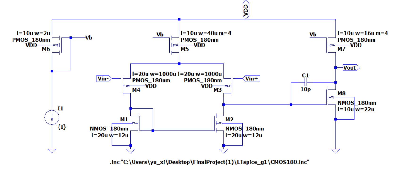
Figure 5. 180nm NMOS circuit
As shown in Figure 5, this is the circuit of an op-amp, with the current mirror M6 powering M5. All the other transistors from M1 to M5 are constituted with primary op-amp structures for amplifying input signals. M7 and M8 constitute secondary op-amp structures. The capacitor, C1, is analyzed with Miller’s theorem after equivalence.
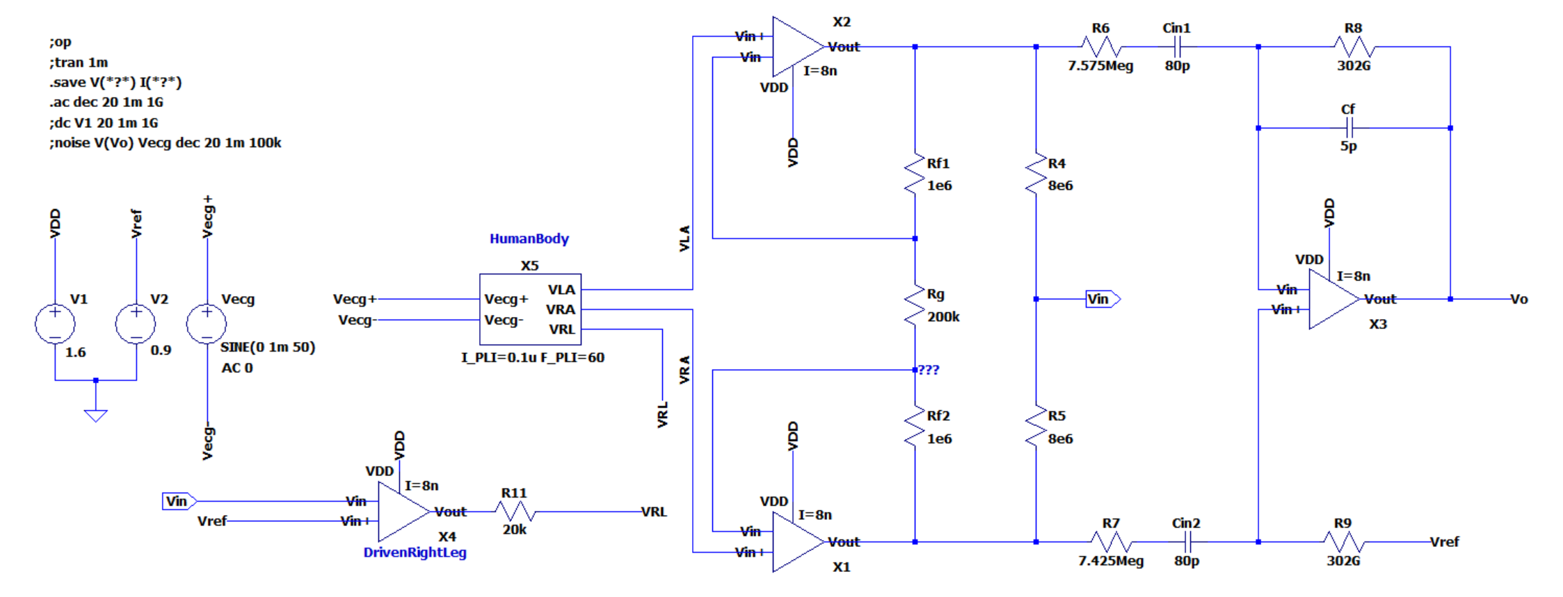
Figure 6. Complete design of the amplification.
As shown in Figure 6, in this design of the comlete amplification circuit, the differential mode gain for stage 1 can be calculated as following:
\( {A_{1}}=\frac{{V_{out}}}{{V_{in}}+(-{V_{in-}})}=R1+\frac{{R_{2}}+{R_{3}}}{{R_{1}}}=20.8dB\ \ \ (5) \)
For stage 2,
\( {A_{2}}=\frac{{V_{0}}}{{V_{in}}}=-\frac{{Z_{f}}}{{Z_{in}}}(\frac{1}{1+\frac{1+\frac{{Z_{f}}}{{Z_{in}}}}{{A_{x3}}}})\ \ \ (6) \)
Let \( {Z_{f}}=\frac{{R_{f}}}{1+S{R_{f}}{C_{f}}},{Z_{in}}=\frac{1}{S{C_{in}}}\ \ \ (7) \)
\( {A_{dm2}}=-\frac{S{R_{f}}{C_{in}}}{1+S{R_{f}}{C_{f}}}(\frac{1}{1+\frac{1+\frac{S{R_{f}}{C_{in}}}{1+S{R_{f}}{C_{f}}}}{{A_{x3}}}})\ \ \ (8) \)
\( \underset{ \begin{array}{c} {R_{f}}→∞ \\ {A_{x3}}→∞ \end{array} }{lim}{{A_{dm2}}=}-\frac{{C_{in}}}{{C_{f}}}\ \ \ (9) \)
3. Results and Discussions
3.1. Simulations based on improved amplification circuit
Based on the newly developed amplification circuit diagram and with the assistance of LTspice, the author simulated the design of the circuit and analyzed the data collected.
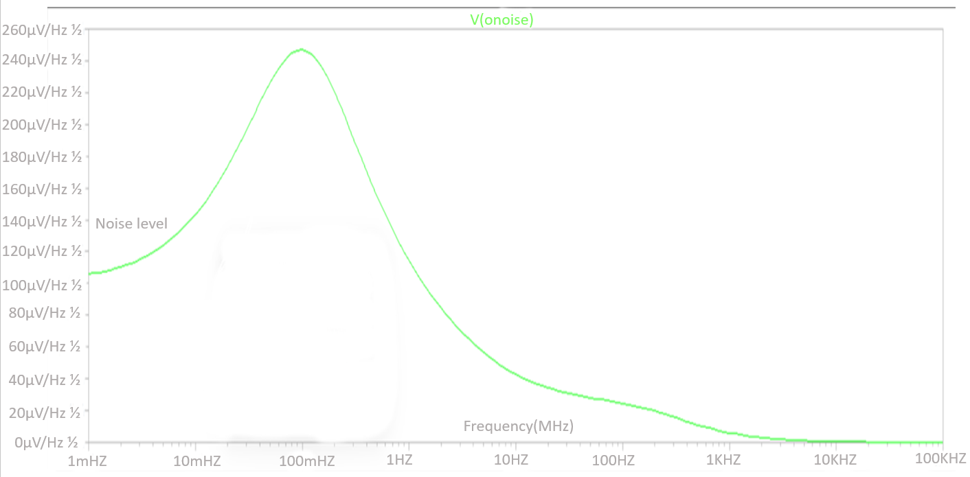
Figure 7. Noise simulation. The continuous line signifies the noise level.
As shown in Figure 7, the total input referred noise can be obtained by the following calculation:
\( Noise= \frac{574.69μV}{{10^{\frac{45dB}{20}}}}=3.23μ{V_{RMS}}\ \ \ (10) \)
which is fairly small. To calculate the noise efficiency factor (NEF), it is required to use formula for NEF:
\( NEF={v_{n, in, RMS}}\sqrt[]{\frac{{I_{total}}}{Φt∙4kT∙BW∙\frac{π}{2}}}\ \ \ (11) \)
For the circuit,
\( {I_{total}}=3.01uA\ \ \ (12) \)
When it is plugged in,
\( NEF=3.23μ{V_{RMS}}∙\sqrt[]{\frac{3.01uA}{Φt∙4kT∙BW∙\frac{π}{2}}}=13.89\ \ \ (13) \)
Next, the simulation also proves the effectiveness of the DRL.
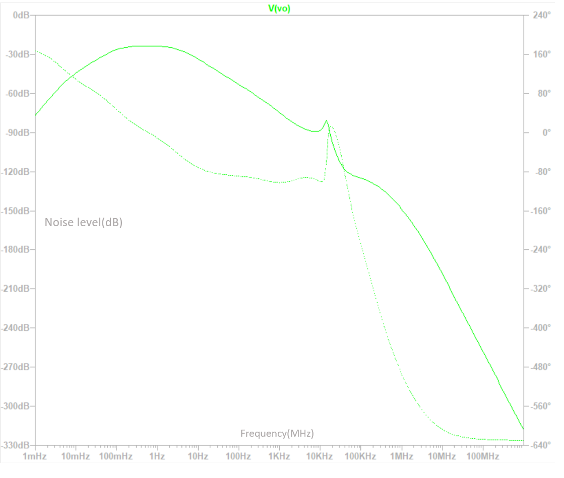
Figure 8. CMG without the DRL circuit. The dashed line signifies the noise level about Vo, while the continuous line signifies the noise level associated with V.
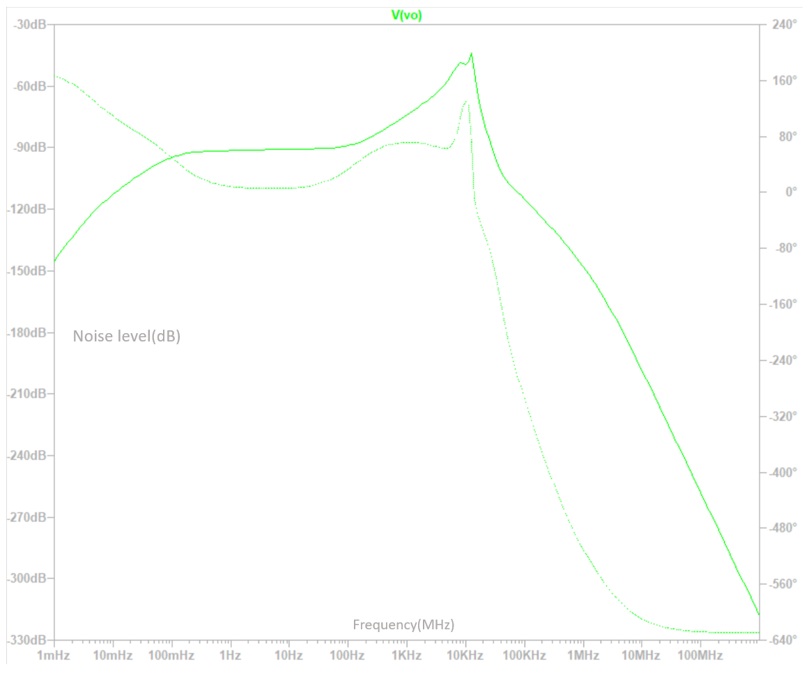
Figure 9. CMG with the DRL circuit connected. The dashed line signifies the noise level about Vo, while the continuous line signifies the noise level associated with V.
As demonstrated in Figure 8, the common mode gain of the system without the DRL circuit is at approximately -48dB when the frequency is at around 50MHz. However, when it is connected to the DRL circuit, as shown in Figure 9, the common mode gain drops to -89dB at the frequency of 50 MHz . This 41 dB difference proves that adding the DRL circuit does have a significant improvement on the common mode gain [10].
At the same time, the common mode rejection ratio is also significantly improved with the DRL. The author first only connected V+ with common mode (VCM) voltage and recorded the result, and then connected V+ with drive-right leg circuit voltage (VRL) to the DRL circuit.
Comparing the value in Figure 8 with Figure 9, the voltage dropped from -47 to -75 dB. Therefore, from this, it is reasonable to conclude that the driven-right leg circuit does help decrease the common mode signal.
3.2. Discussion of the simulation results
Collecting all the results of the circuit based on both hand calculations and LTspice simulations, results are presented as follows:
Table 1. The complete specifications of the amplification circuit.
Specification | Required specs | Results |
Frequency spectrum | 0.1Hz —— 250Hz \( ± \) 10% | 0.11Hz – 249Hz |
Differential gain | 40dB \( ± \) 5dB | 45dB |
Total IRN | < \( 4μ{V_{RMS}} \) | 3.23 \( μ{V_{RMS}} \) |
Total power consumption | < \( 5μW \) | 4.83 \( μW \) |
Total amount of employed capacitance | < \( 1nF \) | 185pF |
All of the data shown proves that the circuit that the author designed and developed satisfies the specifications of being a successful micro-ECG amplifier. The relatively low power consumption of only 4.83 \( μW \) ensures that its battery can last a fairly long period without recharging. The small input referred noise of 3.23 \( μ{V_{RMS}} \) also proves that the amplifier can effectively filter out noise. However, more measures can be taken to improve its working efficiency. Since the amount of current flow in the operational transconductance amplifier (OTA) is associated with the noise level, the power consumption, as well as the common mode gain. Therefore, it takes a lot of effort to find the balance point between these three factors. For further lowering the noise level, approaches such as selecting low-noise components and static operating points of the amplifier. At the same time, the application of differential structure to transmit analog signals and decoupling capacitors at the power output of the circuit can also largely reduce the noise.
4. Conclusion
The current design of the circuit meets all specifications of being a successful ECG amplifier. The small power consumption of only 4.83 \( μW \) ensures that the battery can last for multiple days without any recharge. At the same time, the noise level of only 3.23 \( μ{V_{RMS}} \) proves the effectiveness of this amplification circuit. The design of the electrode also maximizes people’s comfort while wearing this device. Overall, this design of the circuit is a feasible solution for people who have the desire to track their heart condition. The non-invasive design of this device makes it portable and easy to use. The long-lasting battery also makes it perfect for traveling.
Designing a perfect solution to the current problem is never the author’s intention, and some many adjustments and advancements can be made in the future to make this device more powerful and more user-friendly. A pseudo resistor can be used to further improve the circuit. Moreover, since the transistors the author are using is only 180nm, which limits the efficiency of the circuit and the size of the circuit. If there are more advanced manufacturing procedures, the size of the circuit can be further decreased, and the efficiency of the circuit can be largely improved.
References
[1]. Iqbal S M A., Mahgoub I, Du E. et al. 2021 Npj Flex. Electron. 5, 9
[2]. Iskandar A A, Kolla R, Schilling K and Voelker W, 2016 IEEE 18th International Conference on e-Health Networking, Applications and Services, (Munich, Germany: IEEE), 2016, pp. 1-4
[3]. Lee H, Hong Y J, Baik S, Hyeon T, Kim D-H, 2018 Adv. Healthcare Mater. 7, 1701150
[4]. Chatterjee S, Thakur R S, Yadav R N, Gupta L and Raghuvanshi D K. 2020, IET Signal Process., 14 569-590
[5]. Soufineyestani M, Dowling D, Khan A. E. 2020 Appl. Sci. 10 7453
[6]. Kraus W E, Janz K F, Powell K E, et al. 2019 Med Sci Sports Exerc. 51 1206-1212
[7]. Wang N, Zhou J, Dai G, Huang J and Xie Y, 2019 IEEE Trans. Biomed. Circ. Syst., 13, pp. 1112-1121
[8]. Guermandi. M, Scarselli E F and Guerrieri R, 2016 IEEE Trans. Biomed. Circ. Syst., 10, pp. 507-517
[9]. Zompanti A, Sabatini A, Grasso S, Pennazza G, Ferri G, Barile G, Chello M, Lusini M, Santonico M. 2021 Sensors. 21, 2777
[10]. Jedari E, Rashidzadeh R., Mirhassani M. and Ahmadi M., 2017 IEEE 30th Canadian Conference on Electrical and Computer Engineering (CCECE), (Windsor, Canada: IEEE), 2017, pp. 1-4
Cite this article
Yu,X. (2023). The design of the micro-ECG amplification circuit. Theoretical and Natural Science,25,112-119.
Data availability
The datasets used and/or analyzed during the current study will be available from the authors upon reasonable request.
Disclaimer/Publisher's Note
The statements, opinions and data contained in all publications are solely those of the individual author(s) and contributor(s) and not of EWA Publishing and/or the editor(s). EWA Publishing and/or the editor(s) disclaim responsibility for any injury to people or property resulting from any ideas, methods, instructions or products referred to in the content.
About volume
Volume title: Proceedings of the 3rd International Conference on Computing Innovation and Applied Physics
© 2024 by the author(s). Licensee EWA Publishing, Oxford, UK. This article is an open access article distributed under the terms and
conditions of the Creative Commons Attribution (CC BY) license. Authors who
publish this series agree to the following terms:
1. Authors retain copyright and grant the series right of first publication with the work simultaneously licensed under a Creative Commons
Attribution License that allows others to share the work with an acknowledgment of the work's authorship and initial publication in this
series.
2. Authors are able to enter into separate, additional contractual arrangements for the non-exclusive distribution of the series's published
version of the work (e.g., post it to an institutional repository or publish it in a book), with an acknowledgment of its initial
publication in this series.
3. Authors are permitted and encouraged to post their work online (e.g., in institutional repositories or on their website) prior to and
during the submission process, as it can lead to productive exchanges, as well as earlier and greater citation of published work (See
Open access policy for details).
References
[1]. Iqbal S M A., Mahgoub I, Du E. et al. 2021 Npj Flex. Electron. 5, 9
[2]. Iskandar A A, Kolla R, Schilling K and Voelker W, 2016 IEEE 18th International Conference on e-Health Networking, Applications and Services, (Munich, Germany: IEEE), 2016, pp. 1-4
[3]. Lee H, Hong Y J, Baik S, Hyeon T, Kim D-H, 2018 Adv. Healthcare Mater. 7, 1701150
[4]. Chatterjee S, Thakur R S, Yadav R N, Gupta L and Raghuvanshi D K. 2020, IET Signal Process., 14 569-590
[5]. Soufineyestani M, Dowling D, Khan A. E. 2020 Appl. Sci. 10 7453
[6]. Kraus W E, Janz K F, Powell K E, et al. 2019 Med Sci Sports Exerc. 51 1206-1212
[7]. Wang N, Zhou J, Dai G, Huang J and Xie Y, 2019 IEEE Trans. Biomed. Circ. Syst., 13, pp. 1112-1121
[8]. Guermandi. M, Scarselli E F and Guerrieri R, 2016 IEEE Trans. Biomed. Circ. Syst., 10, pp. 507-517
[9]. Zompanti A, Sabatini A, Grasso S, Pennazza G, Ferri G, Barile G, Chello M, Lusini M, Santonico M. 2021 Sensors. 21, 2777
[10]. Jedari E, Rashidzadeh R., Mirhassani M. and Ahmadi M., 2017 IEEE 30th Canadian Conference on Electrical and Computer Engineering (CCECE), (Windsor, Canada: IEEE), 2017, pp. 1-4