


1. Introduction
In order to cope with the energy crisis and environmental pressures, solar energy occupies a major position in the long-term energy strategies because of its abundant energy and ease of use. Photovoltaic cells have therefore become a popular research direction. Among them, photovoltaic cells made of silicon with a crystalline structure account for exceeding 90% of the photovoltaic market. Meanwhile, monocrystalline silicon has a perfect crystal structure and large abundance. In particular, N-type silicon wafers have advantages such as lower impurity and defect concentrations and greater tolerance to optical radiation and thermal effects. High-efficiency cells prepared as substrates have the advantage of superior conversion efficiency and low temperature coefficients. Thus, they are getting more and more attention [1]. The key indicator of the technological level of solar cells is the photoelectric conversion efficiency. Starting in 1954, the first monocrystalline silicon solar cell with an efficiency of 6% was manufactured at the Bell Laboratory in the United States. Efforts to improve the conversion efficiency have been ongoing. In 1976, the Aluminium Back Surface Field (Al-BSF) cell structure was proposed, and the laboratory conversion efficiency reached 15%. In 1999, Passivated Emitter and Rear Locally-diffused (PERL) cell at the University of New South Wales in Australia achieved a conversion efficiency of 24.7%, which reached 25% after the solar spectrum correction. This record has been maintained for fifteen years. The market for solar cells has grown rapidly over the past 15 years. The main body of research now consists of research teams in enterprises selecting technical routes to fulfill technical research. Therefore, both cost and efficiency need to be considered [1,2].
Limited by cost and process, PERL cells have not yet emerged as an industrial battery solution. In 2014, the photovoltaic industry made an important breakthrough. Monocrystalline P-type Passivated Emitter and Rear Cell (PERC) cells are starting to be partially mass-produced in the industry. They gradually replaced the BSF cell technology as the mainstream mass-produced cell technology in 2017. In 2022, the average conversion efficiency will be approximately 23.3%, but the PERC efficiency is approaching the theoretical upper limit of 24.5%. At the same time, due to N-type silicon unique advantages and the development of related efficient technologies, the options for future cell technologies are increasingly rich [2].
2. Principles and theoretical efficiency of solar cells
2.1. Photovoltaic effect
The photovoltaic effect was first discovered in 1839 by French physicist Alexandre-Edmond Becquerel. Solar cells convert solar energy into electrical energy based on the photovoltaic effect. Photovoltaic effect is a specific form of internal photoelectric effect. If the photoelectric effect is understood as two processes: the first is the absorption of light by electrons, and the second is the reaction of electrons after obtaining the energy of light [3]. The focus of this discussion is on the second process: after obtaining energy, if the electron escapes from the surface of the object and becomes a free particle, this is an external photoelectric effect. If the electron is released from the confinement of the nucleus and becomes a free electron in the material, this is an internal photoelectric effect.
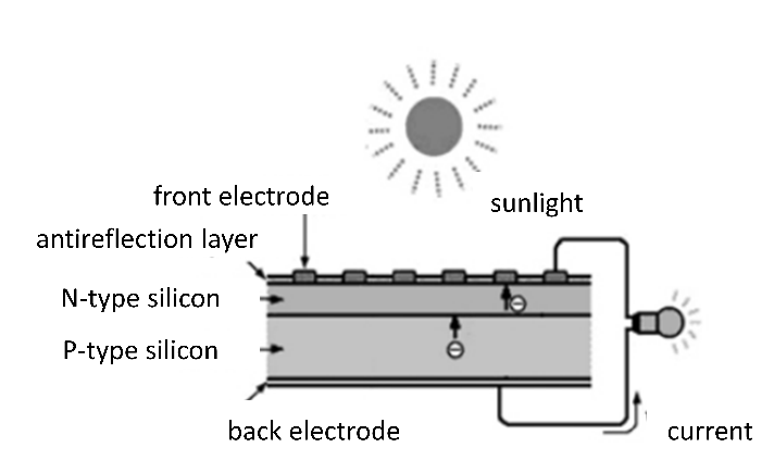
Figure 1. Structure of crystalline silicon cells [4].
The following is combined with the structure of the crystalline silicon cell to elaborate the specific content: as shown in Figure 1. In the preparation of crystalline silicon solar cells, boron is first doped into crystalline silicon to form a P-type silicon wafer. Then, a phosphorus doping process is applied to heavily dope one surface of the silicon wafer, resulting in the formation of a thin layer consisting of N-type, which leads to a p-n junction inside the wafer. In the absence of light, free electrons in the silicon wafer diffuse from the N-type region to the P-type region, forming a diffusion current. The N-type region loses electrons with positive charge, while the P-type region gains electrons with negative charge, forming a built-in electric field. When illuminated by light, the bound electrons absorb the energy of the light and break away from the atomic nucleus, becoming photoelectrons and moving in the silicon wafer. Under the influence of the built-in electric field, photoelectrons in the P-type region will cross the p-n junction and move toward the N-type region. Due to charge accumulation, the p-region potential is higher than the n-region potential. Eventually a voltage is generated between the back electrode and the front electrode. This effect is the photovoltaic effect. When the external circuit is not connected, the voltage difference across the p-n junction is referred to as the open-circuit voltage ( \( {V_{oc}} \) ). When the external circuit forms a direct connection, the current flowing through both ends of the p-n junction is known as the short-circuit current ( \( {I_{sc}} \) ) [3,4].
2.2. Theoretical efficiency
Photoelectric conversion efficiency ( \( η \) ) is a particularly valuable parameter, which is defined as the ratio of the maximum output power of the solar cell ( \( {P_{m}} \) ) to the total incident light power ( \( {P_{in}} \) ) of on the surface of the solar cell. In the standard test environment of solar cells (spectral distribution of m when the air mass is AM1.5, solar irradiance is 1000 \( w/{m^{2}} \) , and temperature is 25℃±1℃), \( {P_{in}} \) considered to be a constant at this time, \( η \) can be written as (1).
\( η=\frac{{P_{m}}}{{P_{in}}}=\frac{{U_{m}}·{I_{m}}}{{P_{in}}} \ \ \ (1) \)
\( {V_{m}} \) and \( {I_{m}} \) denote the voltage and current corresponding to \( {P_{m}} \) . The fill factor ( \( {F_{f}} \) ) is defined as
\( {F_{f}}=\frac{{U_{m}}·{I_{m}}}{{V_{oc}}·{I_{sc}}}. \ \ \ (2)\ \ \ \)
Finally, the expression of \( η \) can be rewritten as
\( η=\frac{{V_{oc}}·{I_{sc}}·{F_{f}}}{{P_{in}}}. \ \ \ (3) \)
It can be concluded from the expression that \( {F_{f}} \) , \( {V_{oc}} \) and \( {I_{sc}} \) are the decisive factors for the photoelectric conversion efficiency. Exploration of extreme efficiency of photoelectric conversion can target how to improve them [4, 5].
3. Characteristics analysis of high-efficiency monocrystalline silicon solar cells
For the loss of battery conversion efficiency, Martin Green has analysed five possible ways as shown in Figure 2: First, when light is emitted to a solar cell, f the photon energy is less than the band- gap width of the cell’s absorption layer, the photon will penetrate directly and cannot stimulate the electron-hole pair. Second, if the photon energy is greater than the band-gap width of the battery absorption layer, the electron-hole pair can be excited, and the excess energy will also cause the electrons and holes to be excited to a higher energy state, which will occur heat with the lattice before formation of the current, and the excess energy will be lost, resulting in the lattice thermal vibration loss. Third, the loss of charge separation and transport of photogenerated carriers in the PN junction. Fourth, the voltage drop loss caused by contact between metal electrode and semiconductor material. Fifth, recombination loss during photogenerated carrier transport [1].
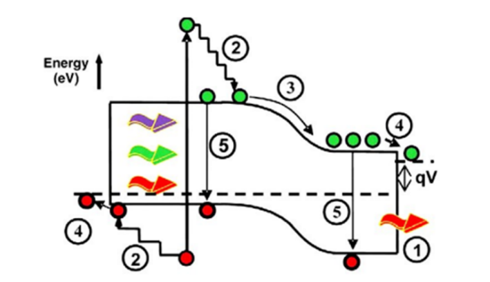
Figure 2. The energy losses in typical solar cell [1].
The above analysis can be summarized as optical loss and electrical loss. Reducing both types of losses effectively improve \( {F_{f}} \) , \( {V_{oc}} \) and \( {I_{sc}} \) and ultimately the conversion efficiency [1]. Methods to reduce optical losses include reflective structures and techniques: such as suede light-trapping structures and optically reflective films. Measures to reduce electrical losses include improving metal contact technology, reducing surface and interface defects with new passivation materials and technologies, improving silicon wafer quality to reduce body defects, adopting special device structures, etc [1]. The following will explore how each of the five types of solar cells can improve against the two losses.
3.1. Passivated Emitter and Rear Cell
In 1989, Martin Green’s research group at the University of New South Wales disclosed the results of a perc-structured monocrystalline silicon solar cell with a laboratory efficiency of 22.8% on a P-type Float Zone silicon wafer. The construction is shown in Figure 3 (a) [1]. It is a natural derivative of the previous generation of yield-dominated Al-BSF cell structures. In the Al-BSF cell, the suppression of the recombination of collective carriers on the Al back-contact surface by the backfield is minimal, making it difficult to reduce the back-contact recombination rate. Moreover, the aluminum layer will partially absorb the infrared bands, reducing the light absorption rate of the cell and limiting its conversion efficiency improvement. Compared to the BSF cell, the Passivated Emitter and Rear Cell (PERC) cell has the following features and advantages. Firstly, optimization of back passivation technology: adding a back passivation dielectric layer between the silicon wafer and the aluminum layer reduces the recombination rate of the back photogenerated carriers. \( {F_{f}} \) , \( {V_{oc}} \) and \( {I_{sc}} \) all increase accordingly. In the meantime, as a back reflector, it increases the long-wave response of the back spectrum of the cell, increases the \( {I_{sc}} \) of the cell, and reduces optical losses. Secondly, the perc cell uses laser slots to form local back electrodes for micro-Nano-level high-precision local contacts, effectively reducing the area of non-passivated regions and ensuring passivation.
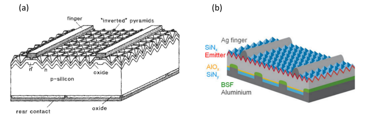
Figure 3. Illustrations of PERC solar cells. (a) Sketch of solar cell in laboratory. (b) Sketch of solar cell in industry [6].
In the preparation process of perc cells, the optimization of back passivation materials and the development of key processes such as back passivation and laser grooving have been ongoing, all of which have contributed to the improvement of conversion efficiency. In terms of the back passivating medium layer, silicon nitride ( \( {SiN_{x}} \) ) was replaced by aluminum oxide (AlO) because of parasitic diverging. Later, an \( {AlO_{x}} \) / \( {SiN_{y}} \) layer stack was a dominant option. The Fraunhofer ISE laboratory proposed laser-based LFC technology, which replaced complex lithography techniques and increased the photoelectric conversion efficiency of PERC cells to 21.3%, followed by the LCO and MWT technologies [6]. Figure 3 (b) shows a typical industrial perc cell. In 2022, by authoritative test of the China Academy of Metrology Science, the conversion efficiency of Hengdian East Magnetic M6 and M10 high-efficiency P-type PERC batteries successfully exceeded 24.01% reaching the highest level in the industry of PERC cell conversion efficiency under current main flow production equipment, materials and processes.
3.2. Tunnel Oxide Passivated Contact solar cell
The Passivated Emitter, Rear Totally-diffused cell (PERT), with n-type silicon wafer as the substrate, the structure is relatively simple, is the earliest n-type battery. At the moment, mass production is at a disadvantage in the light of efficiency and cost compared to PERC cells, and PERT manufacturers will consider upgrading. One of the upgraded solutions based on the Pert battery is the Tunnel Oxide Passivated Contact solar cell (TOPCon) technology.
The main technical features are the preparation of a layer of ultra-thin silicon oxide at the rear of the cell, followed by a coating of doped polysilicon, and finally a metal layer for the electrodes. The three form a passivate contact structure without the need for an opening. In contrast to the perc cell technique, this structure avoids damage to the silicon material caused by the opening, and the carriers migrate from a migration path perpendicular to the contact surface, which may lead to a loss of filling factor at the opening. Among them, the excellent passivation effect of ultra-thin silicon oxide and doped polysilicon causes the energy band atop the exterior of the silicon wafer (as depicted in the illustration provided in Figure 4 (a)), reducing electron transport barrier.
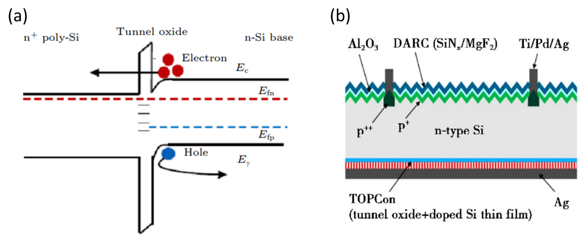
Figure 4 Illustrations of TOPcon cell. (a) Energy band diagram. (b) The structure of TOPCon cell [7].
Due to the quantum tunnelling effect, the ultrathin silicon oxide layer allows the tunnelling of electrons and blocks the passage of holes. The separation of the two reduces the recombination of charge carriers, which effectively increases the \( {V_{oc}} \) and \( {I_{sc}} \) of the cell, thus increasing its efficiency. For ultra-thin tunneling oxide layers, there is another carrier transport theory: the pinhole theory [7]. Based on the result that the interfacial oxide ruptures after thermal annealing, it has been proposed to transport charge carriers through pinholes on the interfacial oxide.
The TOPCon cell was first proposed in 2014 by the Feldmann Institute. As shown in Figure 4 (b), an N-type Float Zone silicon wafer is used. On the front side, silicon nitride passivation is prepared using ordinary pyramidal fleece, boron diffusion, Atomic Layer Deposition of alumina and Plasma Enhanced Chemical Vapor Deposition method to achieve passivation and anti-reflection effect, and on the reverse side, TOPCon technique is used. After optimizing the cell structure, the final cell achieved 700 mV \( {V_{oc}} \) , 82% \( {F_{f}} \) , and 23.7% efficiency. The most critical technology for TOPCon is the fabrication of ultra-thin tunneling oxide layers. Currently, common preparation methods include thermal oxidation, wet oxidation, anodization, plasma-assisted \( {N_{2}}O \) oxidation, etc [1, 7]. The large scale manufacturing efficiency of N-type TOPCon cells in the industry is around 24.5-25%, with a theoretical upper limit of 28.7%.
3.3. Interdigitated back contact cell
The concept of constructing Interdigitated back contact cells (IBC) was initially introduced by Schwartz and Lammert as Figure 5. The salient features of the IBC cell are: Unlike previous types of solar cells, where the electrodes are distributed on both sides of the cell, the IBC cell has a metal-free electrode design on the front that completely avoids electrode obstruction. At the same time, the optically trapped structure consisting of a pyramidal suede structure and an anti-reflection layer on the front surface achieves the optimal design of both the front surface passivation and the surface optically trapped structure, with reduced optical losses and higher \( {I_{sc}} \) [1]. Moreover, the positive and negative electrodes are designed to form an interdigitated arrangement that avoids contact with each other. Optimized electrode grid lines are used to reduce the series resistance. By doing so, the \( {F_{f}} \) is increased.
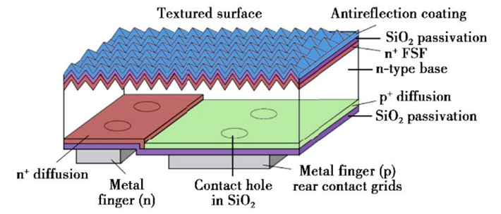
Figure 5. The IBC cell structure mentioned in the paper [1].
A leader in industrial IBC cells, SunPower has developed three generations of IBC solar cells by simplifying and improving back contact cells for large-scale commercial applications. In 2014, an IBC cell with the highest efficiency of 25.2% was fabricated by improving the optical losses at the emitter and back. Similarly, domestic Trina Solar is committed to combining preparation processes to find the best balance between compound and optical losses. In 2018, Trina Solar self-developed 6-inch area (243.18cm²) N-type monocrystalline full back electrode solar cell efficiency reached 25.04%. \( {V_{oc}} \) reaches 715.6 mV. The test results were certified by JET as a third-party test. It represents China’s progress in this field.
3.4. Heterojunction with Intrinsic Thin-layer cell
Heterojunction with Intrinsic Thin-layer (HIT) cells originated from single-sided heterojunction cells studied by Sanyo Corporation of Japan. Later, Hamakawa et al. designed a kind of a-Si/c-Si stacked solar cell. It has the advantage of superior conversion efficiency and reduced temperature sensitivity compared to conventional monocrystalline silicon solar cells. Japan’s Panasonic Corporation is a leader in HIT solar cells. The company increased the cell conversion efficiency to 24.7% in 2013 after continuous optimization and tuning of key technologies such as the transparent conductive oxide layer properties, the amorphous silicon layer resistance loss, and the gate electrodes.
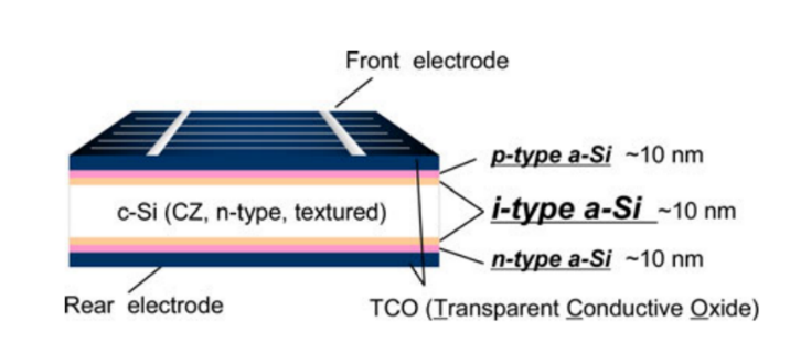
Figure 6. The structure of HIT cell [8].
Figure 6 depicts the Panasonic HIT cell. In order to create a p/n heterogeneous mass junction, intrinsic amorphous silicon and p-type a-Si layer are deposited at low temperatures positioned above Czochralski silicon. The backside field structure is made upon the contrary surface of the wafer using intrinsic amorphous silicon and an n-type a-Si layer. On either side of the doped a-Si an HIT solar cell, there exists a layer of TCO and an electrode composed of a grid made of metal. Using intrinsic amorphous silicon and doped amorphous silicon to accomplish selective carrier transport and full surface passivation, HIT is also a typical selective passivation contact structure like Topcon cells. The advantages of HIT cells are: the a-Si layer is enclosed by a doped a-Si layer and c-Si wafer for more effective passivation of both sides, resulting in higher \( {V_{oc}} \) ; the low-temperature process avoids thermal damage to the battery components etc [8].
In recent years, China has made great progress in HIT cells. By introducing nanocrystallization technology into the doping layer of selective contact of two polar carriers, Longi Green Energy independently created silicon heterojunction cells with a conversion efficiency of 26.81%, which broke all previous records for silicon solar cell efficiency [9].
3.5. Heterojunction with Intrinsic Thin layer and Interdigitated Back Contact cell
In 2014, inspired by the Heterojunction with Intrinsic Thin layer and Interdigitated Back Contact (HBC) structure proposed by Sharp Corporation, Panasonic Corporation combined its HIT cell with the IBC cell structure and eventually developed an HBC cell attaining a level of conversion efficiency that reaches 25.6%. In 2017, its conversion efficiency was further improved to 26.3% and 26.63%, setting a world record. Figure 7 shows the structure of Panasonic’s HBC cell [10].
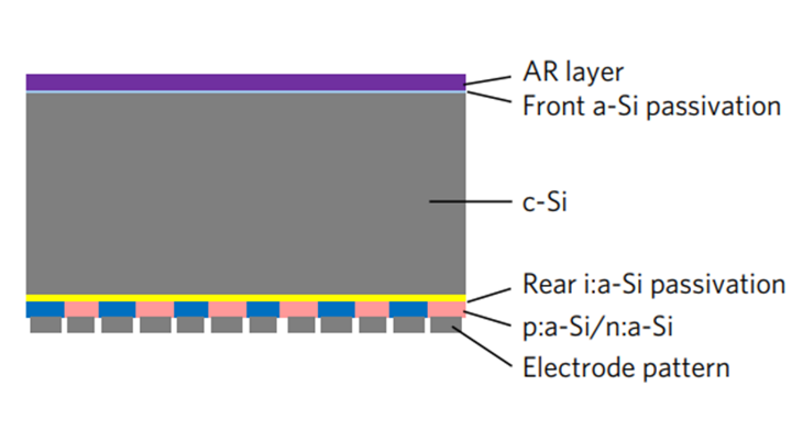
Figure 7. The structure of HBC cell [10].
In general, the advantages and characteristics of HBC are the following. Firstly, improved optical properties: Coating the front surface with an a-Si passivation layer and a dielectric optical antireflection layer. Secondly, improved passive properties: The surface carrier recombination loss can be reduced and the \( {V_{oc}} \) and \( {F_{f}} \) of the cell can be improved by coating the front and back surfaces with a-Si passivation layers, respectively. A local a-Si/c-Si heterojunction structure is formed at back, which totally absorbs the advantages of the amorphous silicon passivation technique for HJT cells. Thirdly, the HBC cells have an IBC cell structure with no black-out losses on the front face and therefore higher \( {I_{sc}} \) [2].
3.6. The present state of battery industrialization across five distinct categories
The mass production efficiency of P-type PERC cells has been gradually approaching the theoretical efficiency limit of 24.5%, and there is limited room for future improvements. The four N-types technical routes TOPCon, HJT, IBC and HBC all have extreme efficiency upper limits. Among them, the TOPCon line has clear advantages. From the current mainstream PERC technology to TOPCon technology, approximately 70% of battery lines are still compatible, allowing for low-cost upgrades. In addition, TOPCon is supported by a complete and sustainable route. In the future, it could be combined with IBC techniques to form Tunnelling oxide passivated contact Back Contact cells and with perovskite cells to form laminated cells. The scope for iterative upgrades is extensive.
HJT has superior mass production efficiency, but the cost of rebuilding the production line and the low-temperature silver paste and metal indium used in the process and technology considerably increases the cost. The advantage of IBC battery comes from the full back electrode, and the disadvantage is also generated. The cross-finger arrangement increases the design difficulty and accuracy; in order to reduce the composite, the passivation of the front surface and the substrate material are required. The process is complicated, the cost increases significantly, so large-scale mass production is difficult. However, its high conversion efficiency and excellent compatibility with battery structures have received a lot of attention. HBC cells represent the highest level of efficiency for crystalline silicon cells, integrating the advantages of both IBC and HJT while retaining the difficulties of the production process, which is complex and costly.
4. Conclusion
Through the analysis of solar cell conversion efficiency, it is concluded that it is mainly determined by \( {F_{f}} \) , \( {V_{oc}} \) , \( {I_{sc}} \) and other parameters. Together with five types of monocrystalline silicon solar cells, exploring ways to reduce optical and electrical losses in various cells to increase the conversion efficiency, taking into account the cost factor. In this paper, it is concluded that with the perc battery approaching the theoretical limit and the development of N-type silicon wafers and corresponding high-efficiency battery technologies, the N-type TOPCon battery technology has huge potential: the production line advantages are obvious, and can realize the low-cost upgrade from the current mainstream perc battery technology. There is a complete sustainable development of the technical route support, and the space for iterative upgrades is wide. Therefore, it is very promising to become a mainstream battery technology after the mass production of perc cells. In addition, the IBC structure can effectively increase the short circuit current. High \( {V_{oc}} \) and \( {F_{f}} \) can be obtained using selective fully passivated contact techniques. Making full use of these two types of technologies, considering the two major loss paths, starting with the three decisive parameters of solar energy conversion efficiency, and relying on the compatibility of various types of batteries, continually innovate and upgrade, and strive to find a balance between cost and efficiency, which is more likely to lay the cornerstone for the industrialization of inexpensive and highly effective monocrystalline silicon solar cells. Finally, this review only discusses the current perc battery technology and the four efficient N-type technologies, and additional efficient battery technologies can be added for comparison in the future to facilitate an in-depth study of the whole.
References
[1]. Chen J F, Zhao S S, Gao T et al. (2019). High-efficiency Monocrystalline Silicon Solar Cells: Development Trends and Prospects. Materials Reports, 33(1), 110-116.
[2]. Deng Q W, Huang Y G, Zhu H L. (2015). Newest Achievement of More than 25% Conversion Efficiency with Crystalline Silicon-Base Solar Cell. Laser & Optoelectronics Progress, 52(11), 1-8.
[3]. Wei S Y, Sun W H, Chen Z J, et al. (2016). The analysis of the efficiency of solar cells. Science China Press, 61(16), 1748-1753.
[4]. Zhang L. (2012). The difference and relation between photoelectric effect and photovoltaic effect. Physics Bulletin, (10), 121-122.
[5]. Yang L L. (2019). Research on Efficiency Abnormality of Crystalline Silicon Solar Cells. Equipment for Electronic Products Manufacturing, 48(6), 1-4,39.
[6]. Dullweber T, Schmidt J. (2016). Industrial silicon solar cells applying the passivated emitter and rear cell (perc) concept—a review. IEEE Journal of Photovoltaics, 6(5), 1366-1381.
[7]. Ren C C, Zhou J K, Zhang B Y, et al. (2021). Status and prospective of high-efficiency c-si solar cells based on tunneling oxide passivation contacts. Acta Physica Sinica, 70(17), 294-304.
[8]. Taguchi M, Yano A, Tohoda S, et al. (2014). 24.7% record efficiency hit solar cell on thin silicon wafer. IEEE Journal of Photovoltaics, 4(1), 96-99.
[9]. Lin H, Yang M, Ru X N, et al. (2023). Silicon heterojunction solar cells with up to 26.81% efficiency achieved by electrically optimized nanocrystalline-silicon hole contact layers, Nature Energy, 8(8), 789-799.
[10]. Yoshikawa K, Kawasaki H, Yoshida W, et al. (2017). Silicon heterojunction solar cell with interdigitated back contacts for a photoconversion efficiency over 26%. Nature Energy, 2(5), 17032.
Cite this article
Mao,J. (2023). Enhancement of efficiency in monocrystalline silicon solar cells. Theoretical and Natural Science,25,173-180.
Data availability
The datasets used and/or analyzed during the current study will be available from the authors upon reasonable request.
Disclaimer/Publisher's Note
The statements, opinions and data contained in all publications are solely those of the individual author(s) and contributor(s) and not of EWA Publishing and/or the editor(s). EWA Publishing and/or the editor(s) disclaim responsibility for any injury to people or property resulting from any ideas, methods, instructions or products referred to in the content.
About volume
Volume title: Proceedings of the 3rd International Conference on Computing Innovation and Applied Physics
© 2024 by the author(s). Licensee EWA Publishing, Oxford, UK. This article is an open access article distributed under the terms and
conditions of the Creative Commons Attribution (CC BY) license. Authors who
publish this series agree to the following terms:
1. Authors retain copyright and grant the series right of first publication with the work simultaneously licensed under a Creative Commons
Attribution License that allows others to share the work with an acknowledgment of the work's authorship and initial publication in this
series.
2. Authors are able to enter into separate, additional contractual arrangements for the non-exclusive distribution of the series's published
version of the work (e.g., post it to an institutional repository or publish it in a book), with an acknowledgment of its initial
publication in this series.
3. Authors are permitted and encouraged to post their work online (e.g., in institutional repositories or on their website) prior to and
during the submission process, as it can lead to productive exchanges, as well as earlier and greater citation of published work (See
Open access policy for details).
References
[1]. Chen J F, Zhao S S, Gao T et al. (2019). High-efficiency Monocrystalline Silicon Solar Cells: Development Trends and Prospects. Materials Reports, 33(1), 110-116.
[2]. Deng Q W, Huang Y G, Zhu H L. (2015). Newest Achievement of More than 25% Conversion Efficiency with Crystalline Silicon-Base Solar Cell. Laser & Optoelectronics Progress, 52(11), 1-8.
[3]. Wei S Y, Sun W H, Chen Z J, et al. (2016). The analysis of the efficiency of solar cells. Science China Press, 61(16), 1748-1753.
[4]. Zhang L. (2012). The difference and relation between photoelectric effect and photovoltaic effect. Physics Bulletin, (10), 121-122.
[5]. Yang L L. (2019). Research on Efficiency Abnormality of Crystalline Silicon Solar Cells. Equipment for Electronic Products Manufacturing, 48(6), 1-4,39.
[6]. Dullweber T, Schmidt J. (2016). Industrial silicon solar cells applying the passivated emitter and rear cell (perc) concept—a review. IEEE Journal of Photovoltaics, 6(5), 1366-1381.
[7]. Ren C C, Zhou J K, Zhang B Y, et al. (2021). Status and prospective of high-efficiency c-si solar cells based on tunneling oxide passivation contacts. Acta Physica Sinica, 70(17), 294-304.
[8]. Taguchi M, Yano A, Tohoda S, et al. (2014). 24.7% record efficiency hit solar cell on thin silicon wafer. IEEE Journal of Photovoltaics, 4(1), 96-99.
[9]. Lin H, Yang M, Ru X N, et al. (2023). Silicon heterojunction solar cells with up to 26.81% efficiency achieved by electrically optimized nanocrystalline-silicon hole contact layers, Nature Energy, 8(8), 789-799.
[10]. Yoshikawa K, Kawasaki H, Yoshida W, et al. (2017). Silicon heterojunction solar cell with interdigitated back contacts for a photoconversion efficiency over 26%. Nature Energy, 2(5), 17032.