


1. Introduction
Digital clocks are an integral part of contemporary life, gracing homes, offices, and public spaces alike. These clocks display time using numerals or symbols, contrasting with analog clocks, which indicate time through rotating hands. Although digital clocks are typically associated with electronic mechanisms, the term “digital” merely denotes the display technique, not the mechanism behind it. This article delves into the design of a digital clock powered by an FPGA board [1].
For decades, Field-programmable gate arrays have been cornerstones in signal processing and embedded systems. Leveraged in diverse realms like digital signal processing, network communication, and embedded systems [2], FPGAs are champions of parallel processing, hardware acceleration, and intricate logic functions. Thanks to their hardware-centric computations, FPGAs often outpace even the swiftest microprocessors. Their in-field reprogrammability, enabling diverse functionalities without physical hardware alterations, and their innate reconfigurable structure positions them perfectly for rapid prototyping and agile development. Compared to Application-specific Integrated Circuits (ASICs), FPGAs are cost-effective and time-efficient [3]. While ASIC designs are resource-heavy and rigid post-design, FPGAs offer shorter design and debugging cycles, expediting time-to-market. Their growing versatility and affordability make them attractive alternatives to ASICs, especially in low-volume applications.
This endeavor harnesses digital circuitry and FPGA technology, utilizing a MOD 60 counter for tracking minutes and seconds, a MOD 24 counter for hours, and a frequency divider and decoder for support [4]. Through programming in Verilog HDL, the digital clock was crafted to display hours, minutes, and seconds in real-time. This clock boasts precision in time computation and display, fitting everyday needs seamlessly. During the nascent design phase of the digital clock, counters coupled with default clocks generated time [5]. A load signal was introduced to modulate each counter’s state, alongside five inputs - MH (minute’s higher unit), ML (minute’s lower unit), SH (second’s higher unit), SL (second’s lower unit), and H (hour) - to personalize time.
Discussing the project’s core, a load signal was added to govern each counter’s state. Every counter’s clear signal linked to the reset, with a divider on the input side and a decoder on the output to project the respective display signal. In the clock’s subsequent section, the second’s lower unit fed into the decimal counter, and its higher unit into the senary counter, creating a base 60 counter [6]. The clock control signal was directed through the frequency divider. Given the 60-unit upper limit for both minutes and seconds, their design structures mirrored each other. Contrarily, the hour segment employed a base 24 counter. The combined output from all counters, paired with the clock control signals, channeled into the decoder, realizing the time display functionality.
2. Relevant theories
Digital Circuit: A circuit that uses digital signals to perform arithmetic and logical operations on digital quantities is called a digital circuit. In this project, we utilize digital circuits to implement the timing and display functions of a clock, achieving the counting and display of hours, minutes, and seconds by utilizing a combination of a frequency divider, counter, and decoder [7].
FPGA: FPGA is a programmable logic device with features such as high flexibility and good reconfigurability. By utilizing FPGA devices, digital circuit design and logic functionality can be implemented.
Verilog HDL: Verilog HDL (Hardware Description Language) is a hardware description language used to describe the structure and behavior of digital circuits. In this project, we utilize Verilog HDL to model and describe various modules of the digital clock, including the clock, counter, and seven-segment display driver.
Seven-segment display: The seven-segment display is a common type of digital display device, consisting of 7 individual LEDs [8]. Each LED represents a segment of a digit, including segments a, b, c, d, e, f, and g. By controlling the on/off state of each segment, different numbers and characters can be displayed.
QUARTUS: QUARTUS is an FPGA design software developed by Altera [9]. It provides an integrated development environment for various functionalities, including Verilog code writing, logic synthesis, and placement and routing. Ultimately, it generates executable files that can be loaded onto an FPGA.
3. System Analysis and Application Research
As for a seven-segment display clock, the following is divided into four sections: overall design, coding process, simulation, and conclusion.
3.1. Overall design
The overall design is unfolded into three parts: second, minute, and hour display modules respectively. The circuit begins with counters and default clocks working to gain the time. Then, a load signal is added to control the state of each counter [10]. There are 5 inputs in all, which are MH (the high part of the minute), ML (the low part of the minute), SH (the high part of the second), SL (the low part of the second), and H (hour), operating as time customizer. The decoder module works as the corresponding display signal. Figure 1 is the overall module based on the circuit diagram.
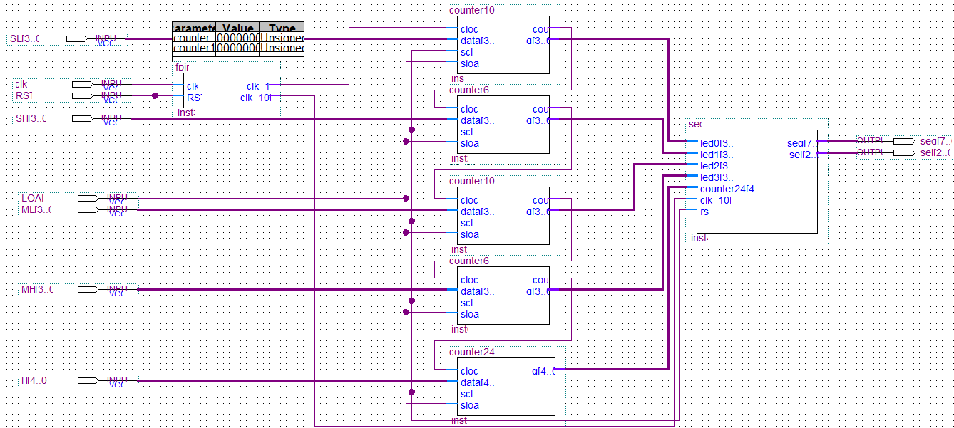
Figure 1. The overall module based on the circuit diagram (Photo/Picture credit: Original).
In general, a load signal serves a function of controlling the state of each counter. The signal which functions to clear the instructions for each counter is connected to the reset signal. When settling the divisor at the input site, it can do as a decoder at the opposite.
Figure 2 and 3 are the circuit design of the second display module. While the low part of the second is put into the decimal counter, the high part of the second is input to the integer counter.
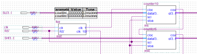
Figure 2. Second display module (Frequency divider) (Photo/Picture credit: Original).
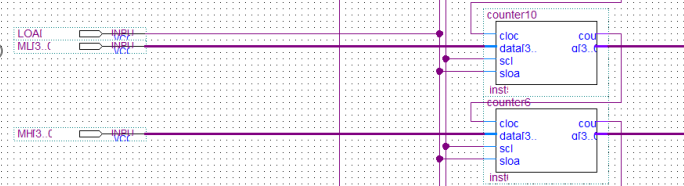
Figure 3. Minute display module (Photo/Picture credit: Original).
Figure 4 is the circuit design of the hour display module. It uses a counter based on twenty-four.
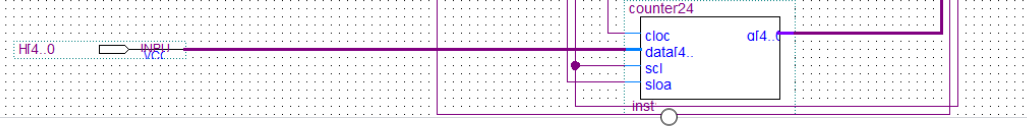
Figure 4. Hour display module (Photo/Picture credit: Original).
Finally, output all signals controlled by counters and clocks to the decoder, and the decoder module will output the corresponding display signal. Shown in Figure 5.
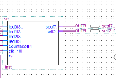
Figure 5. Decoder module (Photo/Picture credit: Original).
3.2. Principles of counters and frequency dividers
Implementing the counter with the LM function can greatly reduce the amount of code-writing work. Use the mega wizard plugin manager to implement the micro function module cause and design the counter parameters. Taking decimal counters as an example. Choose four bits for the bitwise of the output. Round it to a six-bit counter. The minute time adjustment function and the set-up function should have been loaded and selected. Figure 5 shows the design counter module. The process is proximately similar for six-bit and twenty-four-bit counters (the twenty-four counter eliminates the need to select the rounding output). After creating all the counters, they are added to the new project.
The twenty-four counter denotes the mode. When opening the top-level file for responding to the counter, it just produces a frame. Pull the contents of the sub-model and add the exemplification statement to the top level. The frequency divider is generated directly from the code. Since the RPM can’t be achieved, for each frequency, a frequency divider is needed to shift the input signal.
3.3. Decoding module
The decoding module in the quarters is shown in Figure 6, 7, 8 and 9. Inputs include a clock signal, a recess signal, and five data input signals. These five four-input signals correspond to the hours, minutes, and seconds respectively. After all the sub-models are coded, each signal of the sub-model is constructed and connected with the wires.
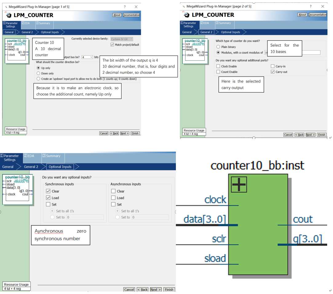
Figure 6. Design of Counter 10 (Photo/Picture credit: Original).
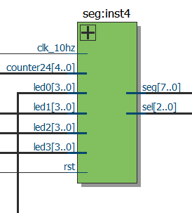
Figure 7. Decoding module (Photo/Picture credit: Original).
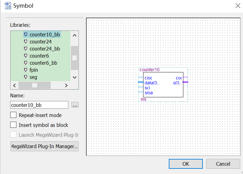
Figure 8. Structure diagram (Photo/Picture credit: Original).
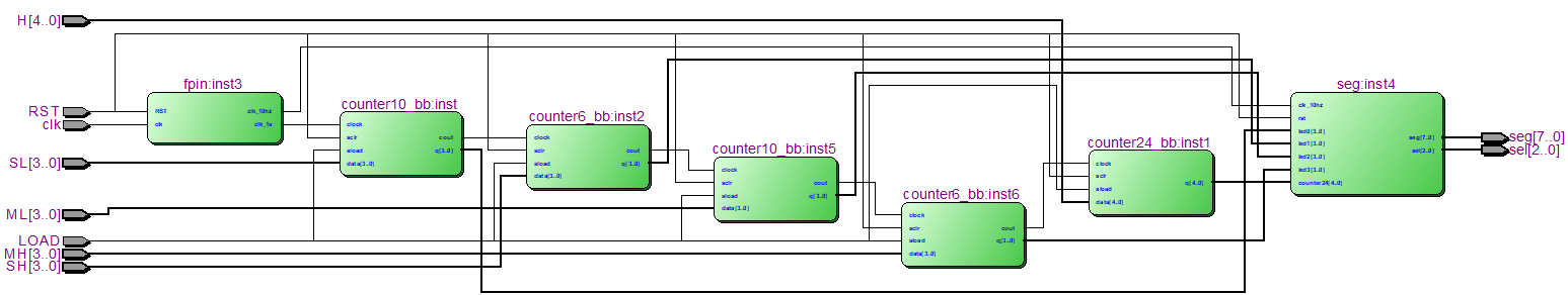
Figure 9. Flowchart (Photo/Picture credit: Original).
3.4. Generate circuit diagrams
The adding process of the test bench and verification of clock running and time setting.
3.5. Application research of 7-Segment Display Clock
Electronic equipment: 7-segment display has a wide range of applications in home appliances, through the use of servo motors, display numbers, and various characters, to provide users with a convenient information display.
Embedded system: In embedded systems, a 7-segment display is also a common display technology to achieve high-precision real-time data updates.
Industrial control: In the field of industrial control, 7-segment displays are widely used in various instruments and controllers because of their flexibility, convenience, and other advantages.
4. Challenges
Hardware Limitations: One often encounters the 7-segment display in electronic devices meant for showcasing numbers and specific letters. But, a notable drawback is its inability to represent all letters and symbols. Designers must be mindful of this constraint when crafting a clock centered around this display. Programming Complexity: The unique nature of a 7-segment display demands tailored programming strategies. To effectively control these displays, ensuring their synchronized operation, appropriate coding is paramount. When the display is expected to convey varied information, such as time, date, or temperature, the programming intricacies can escalate. Maintenance and Calibration: Setting 7-segment displays apart from conventional clocks is their calibration needs for consistent display precision. When glitches emerge, whether in the software or the hardware, specialized know-how and tools become essential for resolution.
User Experience: While 7-segment displays find relevance in certain scenarios, they lack the immediate clarity offered by modern digital or LCD screens, potentially impacting the user’s interaction and satisfaction. Compatibility Challenges: A myriad of devices and coding languages can stipulate unique drivers or interfaces for a seamless dialogue with 7-segment displays, occasionally leading to compatibility hurdles. Real-time Constraints: For some applications, like meteorological predictions or stock market activities, the need for real-time data updates is paramount. 7-segment displays might introduce lags due to their extended processing times for content refreshes.
5. Conclusion
This paper delves into the intricacies of the seven-segment display clock. Initially, the article elucidates the fundamental concept behind the seven-segment display, underscoring its prevalent use in showcasing both numbers and letters. The ensuing sections elucidate the mechanics of the seven-segment display, shedding light on its technical nuances. The piece breaks down the art of translating individual numbers or letters onto seven distinct LED lights through a symphony of logic gates, such as the AND, OR, and NOT gates. It further explores the crafting of a driver essential for dictating the precise display of each character. The narrative meticulously unpacks the algorithms and programming paradigms harnessed to breathe life into the clock functions of the seven-segment display. In culmination, the article trumpets the virtues and merits of the seven-segment display clock, offering insights into potential avenues for refinement to elevate the performance and versatility of this display technology further.
Authors Contribution
All the authors contributed equally and their names were listed in alphabetical order.
References
[1]. Borodzhieva, A. N., Stoev, I. I., & Mutkov, V. A. (2019, May). FPGA Implementation of Code Converters of Decimal Digits from BCD Codes to Seven-Segment Display Code. In 2019 X National Conference with International Participation (ELECTRONICA) (pp. 1-4). IEEE.
[2]. Kumar, M., Jayalaxmi, A., & Malemnganbi, W. (2022). Design and Implementation of Secured Car Parking System using FPGA. International Journal of Applied Engineering Research, 17 (3), 180-188.
[3]. Seetharaman, R., Ramajayam, M., Kamalakannan, K., Vignesh, M., Saran, R. L., Anandan, K., & Mole, S. S. (2022, March). FPGA Based Morse Code Communicator for Visual and Speech Impaired People using Basys-3. In 2022 International Conference on Electronics and Renewable Systems (ICEARS) (pp. 1889-1894). IEEE.
[4]. Qu, L., Wang, C., Sun, W., Lin, Y., & Zhang, H. (2020, September). Design and simulation of three-level SVPWM based on FPGA. In IOP Conference Series: Earth and Environmental Science (Vol. 565, No. 1, p. 012013). IOP Publishing.
[5]. Šušteršič, T., & Peulić, A. (2019). Implementation of face recognition algorithm on field programmable gate array (FPGA). Journal of Circuits, Systems and Computers, 28 (08), 1950129.
[6]. Zhu, X., Xu, H., Zhao, Z., & others. (2021). An Environmental Intrusion Detection Technology Based on WiFi. Wireless Personal Communications, 119 (2), 1425-1436.
[7]. Tsai, M. F., Tseng, C. S., & Cheng, P. J. (2021). Implementation of an FPGA-based current control and SVPWM ASIC with asymmetric five-segment switching scheme for AC motor drives. Energies, 14(5), 1462.
[8]. Sirisha, B., & Kumar, P. S. (2019, October). SVPWM based generalized switching schemes for seven level DCMLI including over modulation operation-FPGA implementation. In TENCON 2019-2019 IEEE Region 10 Conference (TENCON) (pp. 2135-2142). IEEE.
[9]. Minev, P., Kukenska, V., Varbov, I., & Dinev, M. (2022, September). Systems for Remote Access to FPGA Development Boards. In 2022 XXXI International Scientific Conference Electronics (ET) (pp. 1-6). IEEE.
[10]. Seetharaman, R., Shivananth, I., Ganeshakumar, M., Anitha, D., Anandan, K., & Gayathri, S. (2022, November). Development of Crowd Management System using FPGA Circuits. In 2022 International Conference on Augmented Intelligence and Sustainable Systems (ICAISS) (pp. 1-4). IEEE.
Cite this article
Zhang,J.;Zheng,X. (2023). Exploring the implementation and applications of 7-segment clocks on FPGA. Theoretical and Natural Science,26,37-43.
Data availability
The datasets used and/or analyzed during the current study will be available from the authors upon reasonable request.
Disclaimer/Publisher's Note
The statements, opinions and data contained in all publications are solely those of the individual author(s) and contributor(s) and not of EWA Publishing and/or the editor(s). EWA Publishing and/or the editor(s) disclaim responsibility for any injury to people or property resulting from any ideas, methods, instructions or products referred to in the content.
About volume
Volume title: Proceedings of the 3rd International Conference on Computing Innovation and Applied Physics
© 2024 by the author(s). Licensee EWA Publishing, Oxford, UK. This article is an open access article distributed under the terms and
conditions of the Creative Commons Attribution (CC BY) license. Authors who
publish this series agree to the following terms:
1. Authors retain copyright and grant the series right of first publication with the work simultaneously licensed under a Creative Commons
Attribution License that allows others to share the work with an acknowledgment of the work's authorship and initial publication in this
series.
2. Authors are able to enter into separate, additional contractual arrangements for the non-exclusive distribution of the series's published
version of the work (e.g., post it to an institutional repository or publish it in a book), with an acknowledgment of its initial
publication in this series.
3. Authors are permitted and encouraged to post their work online (e.g., in institutional repositories or on their website) prior to and
during the submission process, as it can lead to productive exchanges, as well as earlier and greater citation of published work (See
Open access policy for details).
References
[1]. Borodzhieva, A. N., Stoev, I. I., & Mutkov, V. A. (2019, May). FPGA Implementation of Code Converters of Decimal Digits from BCD Codes to Seven-Segment Display Code. In 2019 X National Conference with International Participation (ELECTRONICA) (pp. 1-4). IEEE.
[2]. Kumar, M., Jayalaxmi, A., & Malemnganbi, W. (2022). Design and Implementation of Secured Car Parking System using FPGA. International Journal of Applied Engineering Research, 17 (3), 180-188.
[3]. Seetharaman, R., Ramajayam, M., Kamalakannan, K., Vignesh, M., Saran, R. L., Anandan, K., & Mole, S. S. (2022, March). FPGA Based Morse Code Communicator for Visual and Speech Impaired People using Basys-3. In 2022 International Conference on Electronics and Renewable Systems (ICEARS) (pp. 1889-1894). IEEE.
[4]. Qu, L., Wang, C., Sun, W., Lin, Y., & Zhang, H. (2020, September). Design and simulation of three-level SVPWM based on FPGA. In IOP Conference Series: Earth and Environmental Science (Vol. 565, No. 1, p. 012013). IOP Publishing.
[5]. Šušteršič, T., & Peulić, A. (2019). Implementation of face recognition algorithm on field programmable gate array (FPGA). Journal of Circuits, Systems and Computers, 28 (08), 1950129.
[6]. Zhu, X., Xu, H., Zhao, Z., & others. (2021). An Environmental Intrusion Detection Technology Based on WiFi. Wireless Personal Communications, 119 (2), 1425-1436.
[7]. Tsai, M. F., Tseng, C. S., & Cheng, P. J. (2021). Implementation of an FPGA-based current control and SVPWM ASIC with asymmetric five-segment switching scheme for AC motor drives. Energies, 14(5), 1462.
[8]. Sirisha, B., & Kumar, P. S. (2019, October). SVPWM based generalized switching schemes for seven level DCMLI including over modulation operation-FPGA implementation. In TENCON 2019-2019 IEEE Region 10 Conference (TENCON) (pp. 2135-2142). IEEE.
[9]. Minev, P., Kukenska, V., Varbov, I., & Dinev, M. (2022, September). Systems for Remote Access to FPGA Development Boards. In 2022 XXXI International Scientific Conference Electronics (ET) (pp. 1-6). IEEE.
[10]. Seetharaman, R., Shivananth, I., Ganeshakumar, M., Anitha, D., Anandan, K., & Gayathri, S. (2022, November). Development of Crowd Management System using FPGA Circuits. In 2022 International Conference on Augmented Intelligence and Sustainable Systems (ICAISS) (pp. 1-4). IEEE.