


1. Introduction
In conventional materials, atoms and molecules organize into ordered, periodic structures in three or two-dimensional space, forming bulk materials with diverse crystal structures. The concept of metamaterials and metasurfaces involves the artificial design of micro/nanostructures, termed "meta-atoms," to mimic the arrangement of atoms and molecules found in natural materials. This artificial structuring imparts unique electromagnetic properties to bulk materials, such as zero or negative dielectric constant, zero or negative magnetic permeability, and zero or negative refractive index, etc. Metasurfaces, specifically, are based on the two-dimensional arrangement of these artificial micro/nanostructures, often referred to as two-dimensional versions of metamaterials. Any two-dimensional surface array with a thickness less than the wavelength of external electromagnetic waves qualifies as a metasurface [1, 2]. Due to their exceptional ability to manipulate optical/electromagnetic fields, lower energy loss compared to metamaterials, reduced space requirements, and lower processing difficulty and cost, metasurfaces have garnered significant attention in various applications, including wireless communication, solar energy harvesting, radar, displays, quantum computing, and biomedical imaging and sensing, etc.
In the last three years, there has been a growing focus on metasurface-based optical biosensors in biomedical sensing research. Over the past few decades, optical biosensors have received increasing attention due to their capability to label samples and provide rapid analysis. They utilize the molecular interactions in response to an incident light at the sensor surface to detect small molecules based on the principles of absorption, emission, scattering, and refractive index variations [3]. Therefore, various optical biosensors such as optical waveguides, optical resonators, photonic crystals, optical fibres, and surface plasmon resonance (SPR) biosensors have been widely explored [3, 4]. The SPR sensor has been widely studied and applied due to the capabilities of real-time monitoring, high sensitivity, and rapid response [5]. However, the traditional SPR biosensors also face challenges like substantial size and limited selectivity in complex biological solutions [6]. Metasurface biosensors, characterized by exceptional optical manipulation capabilities, ease of miniaturization or integration, and multiplexed/multifunctional sensing, emerge as one of the crucial improvements for the next generation biosensing chips.
Given the nascent nature of metasurface-based biomedical sensors, their extensive discussion in recent years has yet to be accompanied by a comprehensive review of new research progress and future directions. This article fills this gap by initially introducing principles in wavefront manipulation and surface resonance, pattern design principles, and performance evaluation indicators for metasurface biosensors. It then meticulously outlines specific applications in biomedical sensing, encompassing blood glucose measurement, virus detection, early cancer detection, and in-situ drug monitoring. The article further delves into mainstream manufacturing technologies for metasurfaces, including the template transfer methods such as projection lithography, nanoimprinting, self-assembly, and direct writing methods utilizing electron beams, ion beams, lasers, or probes. Finally, drawing on metasurfaces' advantages and their potential for commercialization, the article encapsulates future research directions for metasurface biosensors. These include multiplexed and multifunctional sensing, employing all-dielectric metasurfaces for stability and enhanced performance, integrating machine learning for meta-atom design and advanced data analysis, developing miniaturized devices for point-of-care diagnostics, and addressing fabrication challenges for future commercialization.
2. Fundamentals of Metasurface Optical Biosensors
2.1. Wavefront Engineering and Enhanced Light-Matter Interaction
Artificially designed metasurface microstructures demonstrate significant potential for optical wavefront manipulation, a crucial aspect in the design of optical devices. The control of phase plays a pivotal role in wavefront modulation, and metasurfaces excel in introducing an abrupt phase change to the incident wave, enabling effective wavefront modulation [7]. The general relationships between incident and scattered waves are expressed through the generalized Snell’s law of refraction and reflection:
\( \begin{cases} \begin{array}{c} {n_{t}}sin{({θ_{t}}) - {n_{i}}sin{({θ_{i}})=\frac{{λ_{0}}}{2π}\frac{dϕ(x)}{dx}}} \\ {n_{i}}sin{({θ_{r}}) - {n_{i}}sin{({θ_{i}})=\frac{{λ_{0}}}{2π}\frac{dϕ(x)}{dx}}} \end{array} \end{cases} \) (1)
Here \( {n_{i}} \) and \( {n_{t}} \) represent the refractive indices of the two connecting media, \( {λ_{0}} \) is the free space wavelength, \( {θ_{i}} \) , \( {θ_{0}} \) , \( {θ_{r}} \) , and \( {θ_{t}} \) denote the incident, reflected, and transmitted angles and dϕ(x)/dx indicates the phase gradient. This phase gradient is dictated by the geometric structure and distribution of the metasurface plane, and may also be altered by external stimuli.
The achievement of wavefront manipulation relies on enhanced light-matter interaction within the materials through polarizations: the dynamic response of small particles to the external electromagnetic field. These polarizations then induce resonances, and the wavelength of these resonances depends on the sizes, shapes, materials, and surrounding media of the meta-atoms. Meta-atoms with subwavelength scales possess the capability to confine optical field into nanoscale electromagnetic hotspots, a phenomenon commonly referred to as the localization of the optical field. This localized field can also trap analytes within these hotspots due to the influence of the optical gradient force [3]. This unique characteristic enables metasurface biosensors to not only enhance sensitivity, but also pushing the detection limit to single molecules. In the wavefront manipulation process, a phase shift of π can be generated in the resonance process, yet a phase shift of 2π is required for comprehensive manipulation of light properties [8]. Researchers have explored various materials and shapes for both single meta-atoms in periodically arranged metasurfaces and non-periodic metasurfaces to enhance light-matter interactions. For instance, metasurfaces can be designed to manipulate the wavefront using the following approaches [8, 9]:
• Adjusting the geometry and/or size of each micro/nanostructure to alter the characteristics of the wave.
• Huygens’ Metasurfaces: Incorporating nonperiodic micro/nanostructures or multilayered structures to generate secondary waves, either transmitted through or reflected from the metasurface, to obtain varied phase shifts.
• Pancharatnam–Berry (PB) Phase: Tuning the phase shift from 0 to 2π by rotating the orientation direction of the micro/nanostructure.
• Incorporation of Phase Change Materials: Utilizing materials with atomic arrangements switchable between amorphous and crystalline states in response to external thermal, optical, or electrical fields to construct dynamically tunable metasurfaces.
Due to the exceptional wavefront manipulation capabilities, metasurface biosensors have the potential to replace several optical components found in traditional SPR sensors, including prisms, diffraction gratings, beam splitters, polarizers, etc., thereby lead to a simplified system composition and a reduction in size.
2.2. Optical Resonances in Metasurfaces Biosensors
In the last decade, the demand for a rapid and reliable method for monitoring molecular binding, conducting cell studies, detecting cancer, etc., has been imperative. Existing methods, such as PCR, enzyme-linked immunosorbent assay, and mass spectrometry, are time-consuming and require specialized expertise. Metasurface biosensors, comprising plasmonic and/or dielectric micro/nanostructures, offer a novel analytical alternative with the advantages of rapid, label-free, and sensitive detection for various biological samples [8]. The most extensively investigated biosensing strategy with metasurfaces is plasmon resonance, wherein electrons in the metal-based metasurface layer are excited by incident light at a specific angle and then propagate across the metal surface. We should also note that resonance only occurs when the frequency of incident light couples with the intrinsic frequency of the target object. This is attributed to the phase shift in optical waves caused by the enhanced light-matter interaction. In metasurface biosensors, resonance enable label-free, real-time, and non-invasive detection as well as enhance the sensitivity and selectivity of the sensor. Subsequently, the signal detector measures the intensity or angular momentum of the manipulated optical wave, which depends on the refractive indices of analytes near the sensor surface, providing information about target sample concentrations [10]. Building upon plasmon resonance, various enhancements such as surface plasmon polarizations, localized surface plasmonic resonance, and surface-enhanced Raman scattering have been extensively explored to offer strongly confined and enhanced electromagnetic fields for the sensors. In recent years, metasurface biosensors have also expanded to include dielectric metasurfaces based on Mie resonance (resonances of spherical/spheroidal dielectric particles), Fano resonance (coupling between two/multiple resonance modes), etc. These provide comparable sensitivity with superior resonance bandwidth, enhanced quality (Q) factors, better field confinement, and the potential to address the ohmic loss and heating issues associated with current plasmonic sensors, thereby ensuring improved stability and biocompatibility [11, 12].
2.3. Figures of Merit: Sensitivity, Limit of Detection, Selectivity, and Q Factor
To assess the performance of biosensors, various figures of merit are commonly employed. Among them, detection limits or limit of detection (LOD), sensitivity, selectivity, and quality (Q) factor are the most widely recognized. Selectivity is defined as the sensor's capability to detect and differentiate a specific analyte without being influenced by similar or other elements from the whole sample. The primary attribution of this phenomenon is to the distinctive absorption/emission spectrum or chirality of the analytes, which can be enhanced by specially designed meta-atoms. These meta-atoms are strategically designed to induce multi-mode resonances, which are then selectively coupled with the vibrational frequencies of specific analytes [3].
Sensitivity indicates how effectively a sensor responds to changes in analyte concentration which is detected from the change in refractive index of the sample. And the refractive index variations can then be derived from the shifted wave transmission spectrum. Generally, the sensitivity of a biosensor can be quantified as:
\( S=\frac{∆λ}{∆C} \) (2)
Here, Δλ represents the change in peak transmission/reflection wavelength, and ΔC is the change in analyte concentration.
The Limit of Detection (LOD) or Detection Limit (DL) is the minimum analyte concentration detectable by the sensor. In other words, LOD is the minimum amount of analyte required to produce a detectable change in the sensor's output signal. The formula commonly used for determining LOD is:
\( LOD=\frac{3σ}{S} \) (3)
Here, σ is the standard deviation of the control without analyte, essentially representing the system's noise floor, and S is the sensitivity of the sensor. LOD for analyte detection can be specified in various units, with commonly used ones including (1) ng/mL, (2) copies of analyte/mL, (3) PFU/mL, (4) pg/mm2, (5) EID/mL, etc. [13].
The Quality (Q) factor is another crucial aspect for evaluating a biosensor's performance, describing the underdamped condition of an oscillator or resonator and implying the energy loss within a resonant device. The higher the Q factor, the lower the rate of energy loss. The Q factor of an optical biosensor can be expressed as:
\( Q=\frac{λ}{FWHM} \) (4)
where λ is the incident wavelength, and FWHM is the full width at half the maximum of the biosensor’s electromagnetic wave absorption curve [13].
2.4. Metasurface Designs for Biosensors
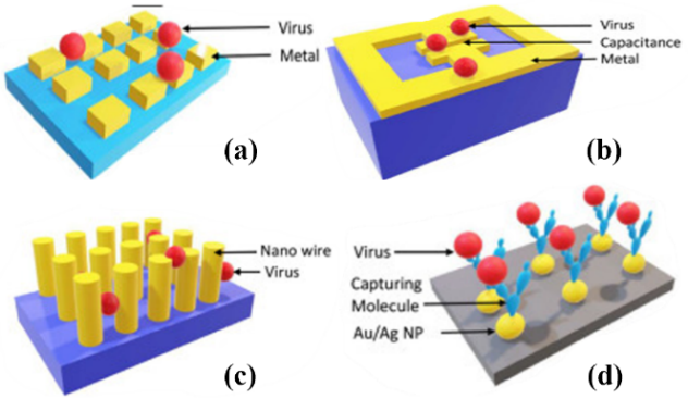
Metasurfaces typically consist of a dielectric substrate and a patterned layer of metal or dielectric micro/nanostructures on top to interact with molecules [14]. The figures below illustrate various plasmonic structures for virus sensing, featuring metal on top and a dielectric layer below. Some of these metal structures can be replaced by dielectric materials to enable all-dielectric sensing. Commonly used materials in the sensing layer include silver, gold, copper, aluminium, titanium dioxide, silicon, germanium, tellurium, and 2D materials such as graphene.
| Figure 1. Schematics of different plasmonic structures for virus detection, including (a, b) planar structures, (c) nanowires, and (d) nanoparticles, respectively. Figures adopted from [14]. |
The conventional design process for metasurfaces involves several steps. Initially, a potential metasurface unit cell with a known wavelength or frequency is established, and lookup tables of the phase (phase maps) are generated by modifying the geometric parameters of the unit cell. Subsequently, the target phase profile Φ(x,y) of the metasurface is created as a function of the spatial position of unit cells with different geometries based on the phase map [8]. However, the conventional direct design approach is time-consuming and not efficient enough for optimization. Researchers have explored an inverse design approach, capable of predicting metasurface structures based on desired optical performance. The steps involve calculating the target optical responses (phase, amplitude, and polarization) at a designated wavelength or frequency using analytical models and finite element simulations. A database of micro/nanostructures is then constructed, linking a given structural geometry to the phases it can provide for specific applications. Finally, the target phase Φ(x,y) is digitized, and a nanostructure from the established database is identified, which imparts a phase φn that matches Φ(x,y) as closely as possible [15].
3. Applications in Biomedical Sensing
3.1. Blood Glucose Measurements
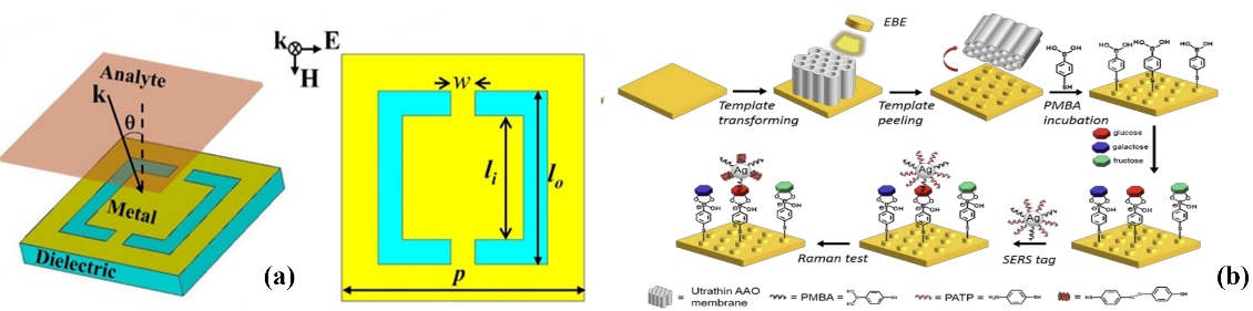
Diabetes, a highly prevalent chronic disease, poses severe risks, including blindness, kidney failure, heart disease, and stroke. According to the World Health Organization (WHO), by 2019, diabetes and associated kidney diseases had led to an estimated 2 million deaths [16]. Therefore, convenient, non-invasive methods for real-time blood glucose monitoring are crucial for managing patients' daily nutrient intake and medication. Normal blood glucose concentrations range between 70 to 120-180 mg/dL. Concentrations below or above this range are classified as hypoglycemia or hyperglycemia, respectively. In recent years, optical methods at different wavelengths, as alternatives to electrochemical methods, have shown high potential for future non-invasive, highly selective, and continuous glucose monitoring [17]. The sensor surface, when exposed to analyte samples containing glucose, experiences a redshift of the resonance frequency and a change in the resonance depth due to the altered dielectric environment. This shift and depth, which corresponds to the refractive index of the analyte, can be used to identify the type of analyte [18]. For instance, Al-Naib introduced a label-free planar terahertz (THz) metasurface comprising arrays of identical split rectangular resonators. The sensor detects glucose concentration ranging from 54 to 342 mg/dL, covering hypoglycaemia, normal, and hyperglycaemia conditions [18]. With a sensitivity of 75,700 nm/RIU, this sensor holds potential applications in both hypocalcaemia and hyperglycaemia cases. Long et al. also presented a surface-enhanced Raman spectroscopy (SERS)-based metasurface containing gold nano-disks, PBMA, and silver nanoparticles, demonstrating good selectivity between glucose and other monosaccharides such as fructose and galactose [19]. The sensor provides stronger SERS signals for glucose due to its unique sandwich-like binding structure with Au nano-disk and Ag nanoparticles.
|
Figure 2. Geometrical schematic of the resonator: (a) 3D representation showing the analyte top coating layer with the incidence angle (θ) of the electromagnetic field and 2D of the symmetric complementary split rectangular resonators with the related dimensions. Figure adopted from [18]. (b) Schematic diagram of the fabrication of the Au-ND metasurface and the corresponding flow chart of glucose detection based on the Au-ND/glucose/Ag NPs sandwich structure. Figure adopted from [19]. |
3.2. Virus Sensing
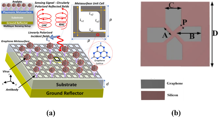
Surface plasmon resonance (SPR)-based immunoassays are widely adopted for label-free biomaterial sensing and clinical diagnostics. Plasmonic biomolecular sensors utilize specific bio-receptors to interact with viruses or viral proteins. These bio-receptors, made of antibodies found in animals, work to identify and neutralize viral proteins or antigens. The surface plasmon resonance can continuously monitor binding kinetics for potential biomolecular activity in real-time by measuring the local refractive index change surrounding the metal. The reactions between biomolecules are enabled by bio-receptors (antibodies) immobilized on the top of the metal surface. The binding event occurs only in the presence of the antigen, resulting in a change in local refractive index. Different types of viruses can be distinguished based on the variations of the reflected polarization states [20]. Some metasurface sensors using localized surface plasmonic resonance (LSPR) have shown the capability to detect various kinds of Avian Influenza (AI) viruses, including H1N1, H5N2, and H9N2 at the same time [20]. Another example is the application of coronavirus detection. A graphene-based plasmonic metasurface presented by Wekalao et al. enables strong light-graphene interactions with a sensitivity of 600 GHz/RIU [21]. This metasurface sensor has benefits, such as a small size, low cost, and also, good compatibility with current detecting systems.
|
Figure 3. Different graphene-based metasurfaces for virus sensing. (a) A graphene L-shaped split ring resonator for Avian Influenza (AI) detection. Different dimensions are given by Lx1=Ly1= 7.5 μm and Lx2=Ly2= 6 μm, and the width of the split ring is 1 μm. The distance between two unit cells (periodicity) is p = 10 μm. Figure adopted from [20]. (b) A Covid-19 detection sensor based on graphene triangular and rectangular structures. The grey region is graphene, and the pink substrate is silicon. Figure adopted from [21]. |
3.3. Early-stage Cancer Discovery
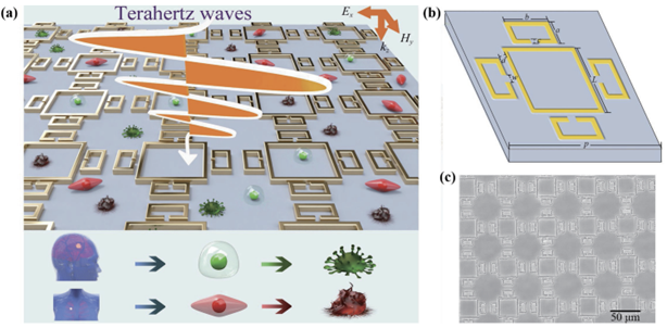
Cancer is a disease with an extremely high mortality rate. Early detection plays a crucial role in the timely treatment and cure of cancer. Current detection methods, such as noninvasive imaging, endoscopy, and ELISA, suffer from several limitations, including low sensitivity, inconvenience, and the risk of perniciousness, which limits the effectiveness of pre-diagnosis and prognosis of cancer. Metasurface biosensors also find applications in cancer biomarker detection, including breast, liver, brain, skin, and oral cancer. In the process of cancer detection, tumour markers (protein markers and non-protein markers) play an important role [22]. Each cancer cell has a particular optical parameter variation due to its internal protein structure, and the refractive index of normal and malignant cells will differ [23]. The change in refractive index helps distinguish between normal and malignant cells. Currently, plasmonic terahertz metasurfaces are widely explored in early cancer detection. Wang et al. presented an ultra-sensitive terahertz metasurface constructed by Au metasurface patterns deposited on a quartz substrate, which has a sensitivity of 504 GHz/RIU [24]. It requires fewer than 10,000 cells to operate with almost a 5-minute detection time, while current clinical technology requires more than 100,000 cells and 20 times longer. The sensor can also successfully distinguish lung and brain cells, leading to a future of early-stage cancer discovery and multiplexed biosensing.
| |
Figure 4. Schematic of the metasurface pattern and the process of detection. (a) Multiple cancer cell types are distinguished by terahertz waves. (b) Unit cell of the biosensor with four C-shaped structures surrounding a rectangular ring structure. (c) Image of the sensor taken by an optical microscope. Figures adopted from [24]. | |
3.4. In-situ Drug Monitoring
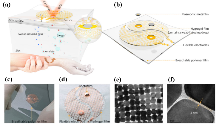
Noninvasive molecule tracking techniques can provide insight into the dynamics of the human body at a more profound molecular level. These capabilities are vital for personalized precision medicine, allowing for more accurate diagnosis and therapy based on an individual’s unique conditions [25]. Molecules in drugs can be identified due to their unique Raman “fingerprint” spectrum. In the past several years, Surface-enhanced Raman Spectroscopy (SERS) sensors have been investigated to detect low concentrations of drug molecules for medical applications. For example, metasurfaces have already shown capabilities of detecting cocaine with concentrations as low as 10 μg/mL with hybrid silver and gold nanoparticles [26]. The most profound research direction nowadays is to directly detect drug molecules through sweat or saliva, as they are speculated to diffuse into secreted biofluids with high degrees of correlation with blood [27]. Liu et al. show a wearable SERS metasurface allowing the detection of drug molecules directly from sweat [25]. The unique construction allows the sensor to sustain various stretches and distortions. Furthermore, the use of SERS also enables the sensor to possess almost “universal” molecular recognition ability.
|
Figure 5. Plasmonic metamaterial–integrated wearable SERS sensing device presented by Liu et al. Figures adopted from [25]. (a) Schematic drawing showing the working principle and design of the device, (b) which consists of two major components (sweat extraction component and SERS sensing component) and was styled to look like a yin-yang symbol. The inset figure highlights the key sensing interface near the metafilm. (c) Optical image of the device and (d) enlarged optical image of the sweat extraction component, which highlights the breathable polymer layer and the plasmonic metafilm. (e, f) High-resolution transmission electron microscopy (TEM) images of the SERS sensing region, which show the plasmonic metafilm is composed of ordered silver nanocube (NC) superlattices. |
4. Advanced Fabrication Techniques
In general, the fabrication of micro/nanostructures involves two approaches: the bottom-up approach and the top-down approach. The top-down approach refers to creating nanostructures by removing some parts of a large entity using an etching or imprinting process, while the bottom-up approach employs evaporating or depositing a thin layer of material on the substrate, together with a lift-off process to build up micro/nanostructures from scratch. It is also inevitable to use both of these two approaches in the process of building complex multilayer constructions in the chip industry. However, for the single-layer metasurface, the selection of top-down and bottom-up processes is much simpler. The truly challenging part is the manufacturing of complicated 2D patterns. The rest of this section mainly discusses the mainstream pattern processing methods as well as some of the emerging methods.
|
Figure 6. Comparison of (a) top-down process and (b) bottom-up process. |
4.1. Template Transfer Methods
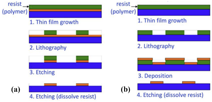
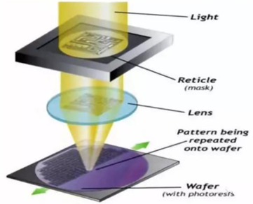
4.1.1. Standard Deposition, Photolithography and Etching. The composition of micro/nano metasurfaces typically involves a silicon-on-quartz substrate, with a thin layer of either metal or dielectric material film deposited via physical vapor deposition or chemical vapor deposition processes. Subsequently, the designed pattern can be transferred using photolithography, followed by the removal of excess material through development and etching processes. Alternatively, pre-patterned photoresist or sacrificial layers can be prepared on the substrate using photolithography or self-assembly processes. Once materials are deposited, the sacrificial layer and excess material are removed through a lift-off process. This set of micro-nano processing techniques is extensively employed in semiconductor chip manufacturing and is highly mature. Despite its high cost, due to its large-scale micro-nano processing, rapid manufacturing capabilities, and mature industrial supply chain, this process is anticipated to become the primary manufacturing method for future commercialized optical metasurface electronic products, transitioning optical metasurface devices from laboratory to mass production applications. The more critical steps in this process include projection photolithography and etching processes. Projection Photolithography (PPL) involves transferring geometric patterns from a photomask onto a substrate using the interactions of incident light with photoresist. Ultraviolet light passes through the photomask and incident on the surface of the photoresist in a stepper or scanning manner. Then, the photoresist in the exposed area undergoes chemical reactions, and through development technology, photoresist in the exposed area (positive resist) or unexposed area (negative resist) is removed, allowing further pattern fabrications on the substrate using etching and deposition techniques [28, 29]. For etching techniques, commonly used processes include plasma etching and other dry etching methods, such as reactive ion etching and deep reactive ion etching. Compared to wet etching, these dry etching techniques offer the advantages of directional etching, providing a larger aspect ratio and more vertical sidewalls. However, due to the wavelength limitations of light, to achieve higher resolutions, shorter wavelength light sources and more advanced immersion exposure systems in the semiconductor industry are required, which have lower degrees of freedom, higher costs, and require EBL or other direct writing methods for mask preparation.
| Figure 7. A schematic of typical projection lithography used in the chip manufacturing industry. |
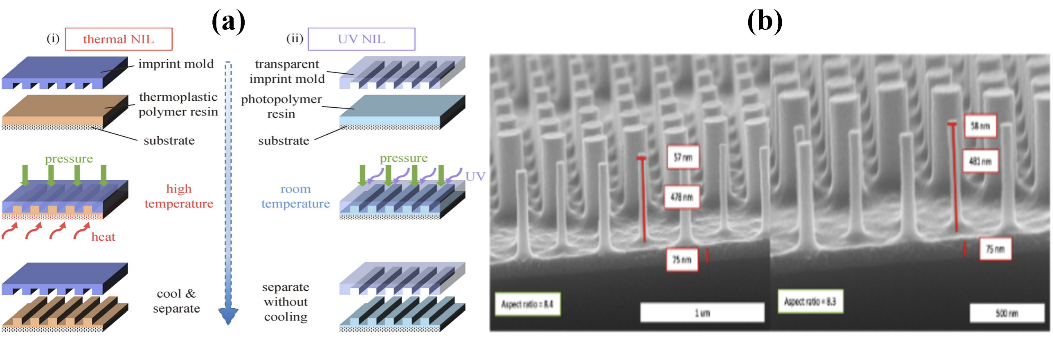
4.1.2. Nanoimprint Lithography. Nanoimprint Lithography (NIL) is a technique that utilizes mechanical deformation to replicate nanostructures. It has the advantages of high resolution (10 – 100 nm), large-area processing, and cost-effectiveness. However, it necessitates high-resolution equipment for template (mold) fabrication. Traditional NIL comprises hot embossing and ultraviolet (UV) embossing. In hot embossing, materials with low viscosity at high temperatures are employed. The template is pressed onto the substrate coated with a polymer layer, solidifying the polymer through heating and cooling. After template separation, the NIL pattern transfers to the substrate, followed by additional etching and polymer removal processes. UV embossing, conducted at room temperature, uses ultraviolet light to solidify the polymer layer during the imprinting. It generally boasts higher productivity due to its straightforward system and rapid response time, eliminating the need for a heat source [30]. Nanoimprint lithography stands out for its cost-effectiveness and high throughput. A significant limitation of conventional nanoimprint is its lower maximum aspect ratio compared to lithography combined with reactive ion etching for the lift-off method. However, Einck et al. introduced a nanoimprinted nanostructure for meta-lenses with UV light solidification, achieving an aspect ratio of ~ 8.4, which addressed this limitation [31]. Current research for industrial production turns toward solving the problems of residual imprinting polymer left on the device after the removal of imprinted polymer, which might impact the optical performance of the surface, and also, the uneven pressure distribution during the large area imprinting.
|
Figure 8. (a) Conventional nanoimprint lithography (NIL) and its replicating performance. Schematics of (i) thermal NIL and (ii) ultraviolet (UV) NIL. Figure adopted from [30]. (b) Cross-sectional SEM images of nano-imprinted structures with height and width, along with the calculated aspect ratio. Figure adopted from [31]. |
4.2. Direct Writing Methods
4.2.1. Electron Beam Lithography. Electron Beam Lithography (EBL) is a method with the capability to directly draw each micro/nano pattern onto the photoresist based on the design, eliminating the need for a photomask to preset the pattern. It involves directing a focused beam of electrons with extremely short wavelengths onto the photoresist, which is sensitive to electrons. The electron beam lithography system offers ultra-high resolution (achieving an extreme feature size of <10 nm) and flexible drawing (enabling direct writing without a mask) [28]. Due to its high resolution and considerable degree of freedom, aligning well with the processing requirements of periodically or non-periodically arranged micro/nano structures, EBL has become the most widely used method in the fabrication of metasurface-based optical sensors. However, the drawback of this maskless lithography technology is that it is time-consuming to prepare large-area complex patterns, resulting in low yield. As of now, its applications are primarily limited to mask manufacturing and the device research and development stage [28].
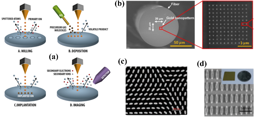
4.2.2. Focused Ion Beam Processing. Focused Ion Beam (FIB) processing is another high-resolution and maskless direct writing technology. This method involves removing atoms from the target surface to create patterns by bombarding the surface with an ion beam without the need for photoresist. Because of its purely mechanical processing, FIB has no material selectivity requirements, theoretically allowing it to process any metal and non-metal [28]. The heavier ions used also result in relatively large etching depth and width. Moreover, the ion beam can bombard gaseous precursors, causing decomposition and direct deposition of materials on the sample surface, granting FIB both bottom-up and top-down manufacturing capabilities. With its exceptional degree of freedom, FIB can also be applied to micro/nano fabrication on rough surfaces or the lateral sides of targets. Sloyan et al. demonstrated the use of FIB in processing metasurface micro/nanostructures at various locations of optical fibers, including the end (lab-on-tip), surface (lab-around-fiber), and inside (lab-in-fiber), thereby enhancing light coupling in optical fibers [32]. However, due to the larger beam diameter of FIB which utilizes ions like Ga and He, its resolution is slightly lower than the EBL, which ranges from 20 to 100 nm. Additionally, the relatively slow processing speed and high cost make this fabrication method more suitable for the proof-of-principle applications in small-area metasurfaces design, fabrication of lab-on-fiber devices, and chip repair [28, 32].
|
Figure 9. (a) Schematics illustrating different applications of focused ion beam processing, including pure mechanical milling, material deposition, ion implantation, and real-time monitoring using SEM during the FIB process. The orange areas indicate the ion source directing ion particle beams toward the substrate. (b) SEM images of non-periodic chiral metasurface and (c) periodic ellipse-shaped structures fabricated by FIB. (d) SEM images of gold nanoarray structures fabricated on the tip of an optical fiber using FIB. Figures adopted from [29] and [32]. |
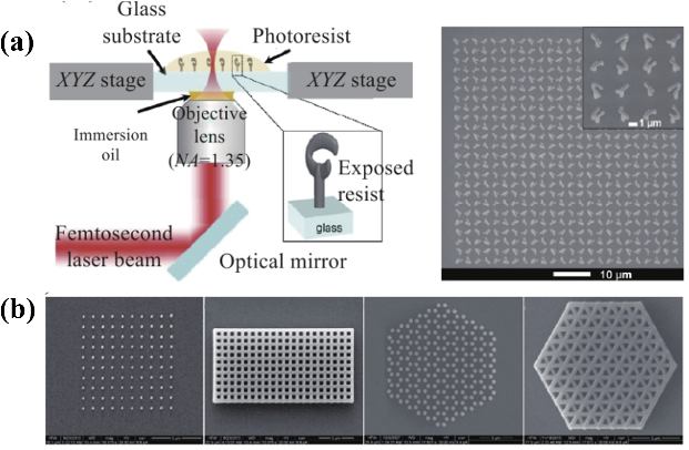
4.2.3. Direct Laser Writing. Direct Laser Writing (DLW) is a technology that employs laser beams to directly scan and process materials, offering the advantages of being maskless, highly flexible, cost-effective, and relatively faster processing. Based on different material processing mechanisms in direct writing, DLW can be further categorized into continuous laser direct writing, ultrafast laser direct writing, and two/multi-photon direct printing technologies. Direct laser writing utilizes a laser beam with adjustable intensity for scanning exposure to the photoresist, creating the desired patterns. Subsequently, etching or thin film deposition is employed to build up the patterns on the substrate. However, the resolution of DLW processing is constrained by the optical diffraction limit, restricting its application to infrared to terahertz waves (760nm - 3mm) [28]. Ultrafast laser direct writing utilizes ultra-fast energy pulses at femtosecond levels to interact with materials in an extremely short period, well below the material's thermal relaxation time, thereby avoiding photothermal effects and potential damage. Two/multi-photon printing exploits the characteristics of two/multi-photon absorption of materials to achieve polymerization in any area within photosensitive materials [28]. This method can define features smaller than those achieved with conventional single-photon polymerization, with a resolution reaching 100 – 200 nm. Due to the two/multi-photon absorption phenomenon and ample radiation, it can not only fabricate materials that are challenging to mechanically machine but also realize 3D printing. This capability extends to processing devices with more complex or even three-dimensional structures. However, in comparison to previously mentioned direct writing technologies, the resolution of direct laser writing is relatively lower. Nevertheless, it still offers the advantages of slightly shorter processing times and reduced processing costs.
| Figure 10. Schematics of different plasmonic structures for virus detection, including (a, b) planar structures, (c) nanowires, and (d) nanoparticles, respectively. Figures adopted from [28]. |
4.2.4. Other Novel Methods. For emerging fabrication methods, table 1 provides a concise overview of self-assembly lithography, scanning probe lithography, plasmonic lithography, and laser-induced forward transfer and ablation. Each entry includes information on the fabrication principle, advantages and disadvantages, extreme resolution, and key attributes.
Table 1: List of other novel fabrication methods including Self-assembly Lithography (SAL), Scanning Probe Lithography (SPL), Plasmonic lithography, and Laser-induced forward transfer and ablation. Information accessed from [28, 29]. | ||||
Method | Fabrication Principle | Advantages & Disadvantages | Extreme Resolution | Attributes |
Self-assembly Lithography (SAL) | Using an array of polystyrene spheres formed by colloidal self-assembly to act as a mask template in combination with subsequent etching or deposition processes to fabricate micro/nano structures. | • Simple process; low cost; large area processing • Only extremely simple structures can be processed | hundreds of nm | Template transfer |
Scanning Probe Lithography, SPL | Using a nano probe to move particles on the material surface, which is controlled by an atomic force microscope. | • Ability to process extremely small sizes; Simple process • Low processing efficiency; low aspect ratio | <10 nm | Direct writing |
Plasmonic lithography | Insert a dielectric layer between the mask and photoresist coated substrate, normal incident light excites free-electron oscillations resulting in surface plasmon polarization to confine optical fields to smaller wavelength. | • high processing efficiency; address the limitations of conventional light diffraction • short working life; poor fidelity; large-area photomask still needs to be addressed | ~100 nm | Template transfer |
Laser-induced forward transfer (LIFT) | Pulsed laser beam pass through transparent substrates and apply optical energy to the material, which is then transformed into kinetic energy. The illuminated material is ablated and deposited on an opposite receiver substrate. | • Compatible with a broad range of materials; low-cost; simple set up and operations; no clean room requirement • Low bonding strength between coatings and substrate | ~100 nm | Direct writing |
These methods showcase diverse approaches to fabrication, each with its unique set of advantages and challenges, catering to specific requirements in the development of metasurface-based optical sensors.
5. Challenges and Outlook
5.1. Multiplexing and Multifunctional Sensing
As discussed in Section 3, recent research indicates that metasurface-based optical biosensors have the potential to detect and distinguish various types of analytes simultaneously. It is evident that multiplexing and multifunctional sensing represent promising avenues for the future of biomedical sensing. For instance, current sweat-based electrochemical sensors, measuring currents or potentials at electrode surfaces to transduce analyte concentrations, can continuously track electrolytes (K+ and Na+), metabolites (lactate and glucose), and drugs in sweat. However, these sensors are often limited to detecting one analyte at a time [25]. One solution involves integrating different sensing platforms on a single chip to achieve multiplexed sensing [33]. In contrast, metasurface optical biosensors can simultaneously detect various molecules without requiring separate addition of different sensing platforms. This capability arises from their unique interactions with incident light, resulting in diverse changes in spectral signals. This potential opens avenues for designing an almost "universal" sensing platform capable of detecting a range of analytes in sweat. It also allows the design of biosensors capable of simultaneously sensing similar yet distinct elements, such as various types of avian influenza, coronaviruses, or cancers. The simultaneous detection of multiple targets could become a distinctive feature of the next generation biosensors.
5.2. All-Dielectric Metasurfaces
While plasmonic materials can offer robust optical resonances, a natural limitation arises in the form of ohmic loss (resistive loss). This phenomenon involves the transfer of incident light energy to heat dissipation within the material, caused by the decay of coherent electron charge density oscillations on a metal-dielectric interface [8, 34]. This characteristic renders plasmonic materials nonideal for high-efficiency devices and may pose risks, particularly in wearable and implantable devices. The distinctive advantage of all-dielectric metasurface sensors lies in their generally low intrinsic damping, resulting in significantly narrower full-width at half-maximum (FWHM) resonances and enhanced quality (Q) factors [12].
5.3. Machine Learning for Meta-Atom Design and Enhanced Data Analysis
Machine learning, a rapidly advancing field, has shown promise in applications across chemical, biological, mechanical, and materials engineering. Its core advantage lies in its ability to autonomously discern the relationships between input data and target data, drawing insights from past experiences without explicit guidance from well-defined physical laws that explain these connections [35]. This capability holds significant potential for the inverse design of meta-atoms. The approach involves collecting an extensive dataset comprising various meta-atom structures and their corresponding electromagnetic (EM) responses from prior research. This dataset is then utilized to train a deep neural network, enabling it to uncover the intrinsic rules governing the relationship between a meta-atom building block and its EM properties. Through comprehensive training, the network becomes adept at calculating arbitrary EM responses based on the provided structural data. Simultaneously, an inverse network is developed, offering the ability to optimize the design of a meta-atom in terms of its geometric parameters. While the effectiveness of this approach is influenced by the size of the training data, limiting the degrees of freedom for new shape designs, enhancements such as physics-informed neural networks and topology optimization can address this limitation. These improvements integrate physical laws of advanced optical theories, providing more degrees of freedom to output nearly arbitrary meta-atom shapes and less training time [36]. Moreover, machine learning algorithms prove valuable in processing spectral signals obtained from the signal detectors. Biosensors, particularly plasmonic sensors, often exhibit spectral amplitude fluctuations due to the light source variations or spectrometer influences. Through extensive training on raw data and engineered data, machine learning algorithms can effectively filter out those noise and fluctuations. This not only reduces the rely on stable and costly hardware but also enhances the robustness of signal measurements in biosensors [37].
5.4. Point-of-Care Diagnostics
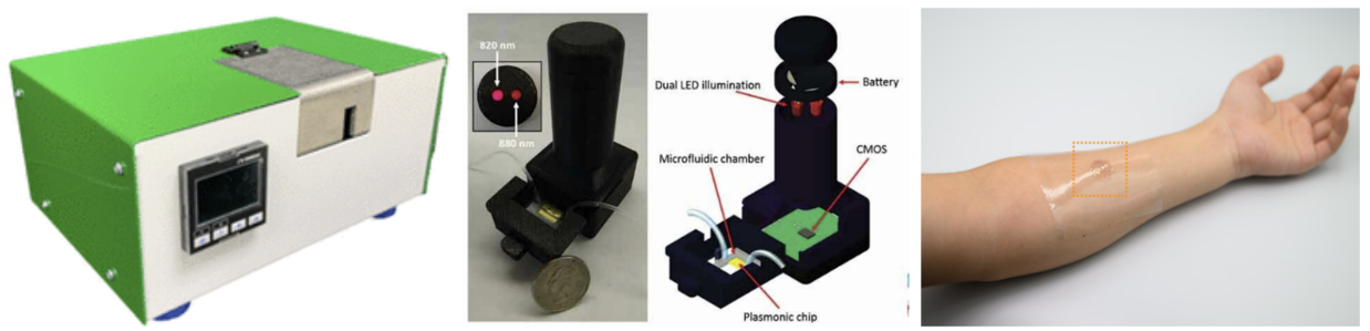
Point of care testing (POCT) represents the ability to conduct diagnostics without the need for a traditional laboratory or extensive medical infrastructure. Instead, these tests are performed in close proximity to the patient. In contrast to conventional processes where samples are sent to laboratories for analysis, point-of-care diagnostics allow physicians or even patients themselves to swiftly process medical samples and obtain real-time results. Metasurface optical biosensors, showing label-free, non-invasive, and real-time molecular analysis capabilities, hold significant promise for the development of user-friendly, automated, and portable instruments for point-of-care diagnostics. The integrated system typically comprises microfluidics which transport analytes to the sensor's surface, LEDs or lasers for the light source, a CMOS or quadrant detector, a data processor, and a battery [38, 39]. As illustrated in Figure 11, these components can be compactly arranged, enabling the creation of portable devices that can be effortlessly transported. Additionally, the exploration of wearable metasurface optical biosensors presents another direction, although they are currently underexplored. These devices aim to detect analytes directly from human sweat, with the metasurface layer deposited on a flexible polymer layer to allow bending. An essential criterion is the sensor's ability to withstand mechanical strains and distortions induced by human skin without a noticeable decline in performance. For instance, the SERS sensor developed by Liu et al. [28] maintained stable SERS activity under a maximum strain of ~50% and after 1000 stretching-relaxation cycles at 30% strain. Ongoing research needs to focus on innovative pattern design and novel device packaging strategies to determine the feasibility of commercializing wearable metasurface sensors.
|
Figure 11. Examples of Miniaturized Portable and Wearable Sensors. Figures adopted from [38], [39], and [28] successively. |
5.5. Challenges in Fabrication and Commercialization
Current optical metasurfaces have predominantly focused on verifying new principles and functions. However, a considerable performance gap exists between the fabricated devices and their simulation results, such as the reduced beam diffraction and deflection efficiencies. This disparity arises from various fabrication errors, including intrinsic material property discrepancies, size deviations, shape errors, and the loss of meta-atom integrity in existing fabrication processes [28, 40]. For the practical application of metasurfaces, a comprehensive investigation into the relationship between fabrication errors and device performance is essential. Identifying the causes of errors in different fabrication techniques and optimizing processes is vital to guide the industrial production of metasurface-based devices.
Accelerating the evaluation and development of fabrication techniques suitable for metasurface production is also imperative. This involves establishing a metasurface processing supply chain or integrating metasurface production into the current semiconductor industry. While current direct writing methods are suitable for small-area verification in scientific research, highly customized products, or the fabrication of photomasks and nanoimprint templates, mass industrial production demands large-area template transfer technologies such as projection lithography, nanoimprinting, or self-assembly. However, the projection exposure technology used by the semiconductor industry faces challenges related to high costs, limited degrees of freedom, and lower customization capabilities, making it suitable primarily for products with substantial market demand. Nanoimprint technology needs to address issues like residual imprinting polymer and enhance large-area imprinting results. Meanwhile, self-assembly can only fabricate simple and periodically arranged structures. To overcome these challenges and facilitate the commercialization of metasurface biosensors, proactive exploration of highly demanded surface morphologies and materials is necessary. Selections of appropriate fabrication techniques should align with diverse material, structure, and arrangement requirements. Simultaneously, efforts should be intensified to address existing challenges and innovate novel fabrication methods. These initiatives collectively contribute to advancing the field and paving the way for the practical application of metasurface biosensors.
6. Summary
The exploration of artificially designed metasurfaces in biomedical sensing has emerged as a novel research field over the past three years. These metasurfaces demonstrate the ability to manipulate wavefronts by inducing abrupt phase changes to incident electromagnetic waves. This manipulation is achieved through various means, including adjusting the shapes, sizes, arrangements, and orientation angles of the meta-atoms or employing phase-change materials, resulting in remarkable light-matter interactions. Recent research indicates that metasurface biosensors, in addition to offering rapid, label-free, and sensitive detection for diverse biological samples, can address challenges faced by traditional Surface Plasmon Resonance (SPR) sensors. These challenges include limited capability in distinguishing analytes in complex solutions and difficulties in miniaturization. The accomplishments in metasurface biosensors pave the way for the development of the next generation high-performance, multifunctional biosensors tailored for point-of-care diagnostics. Additionally, the application of all-dielectric metasurfaces shows potential in mitigating issues related to Ohmic loss and heat dissipation inherent in current SPR sensors, thereby offering a solution for designing more stable devices. In the realm of meta-atom design, machine learning emerges as a powerful tool, demonstrating proficiency in inverse design of meta-atoms based on desired electromagnetic responses. This capability significantly reduces the time spent on research for future product development. Furthermore, a thorough examination and comparison of fabrication techniques for metasurfaces reveal that, while direct writing methods are prevalent in laboratory-based metasurface fabrication, template transfer techniques, characterized by high throughput and cost-effectiveness, present a more suitable solution for the mass production of commercially viable metasurface devices. However, it is essential to address the challenge of understanding the relationship between fabrication errors and device performance before the successful commercialization of metasurface biomedical sensors.
References
[1]. C. L. Holloway, E. F. Kuester, J. A. Gordon, J. F. O’Hara, J. C. Booth, and D. R. Smith, “An overview of the theory and applications of metasurfaces: the Two-Dimensional equivalents of metamaterials,” IEEE Antennas and Propagation Magazine, vol. 54, no. 2, pp. 10–35, Apr. 2012, doi: 10.1109/map.2012.6230714.
[2]. X. Luo, “Principles of electromagnetic waves in metasurfaces,” Science China Physics, Mechanics & Astronomy, vol. 58, no. 9, Sep. 2015, doi: 10.1007/s11433-015-5688-1.
[3]. J. Qin et al., “Metasurface Micro/Nano-Optical Sensors: Principles and Applications,” ACS Nano, vol. 16, no. 8, pp. 11598–11618, Aug. 2022, doi: 10.1021/acsnano.2c03310.
[4]. C. Chen and J. Wang, “Optical biosensors: an exhaustive and comprehensive review,” Analyst, vol. 145, no. 5, pp. 1605–1628, Jan. 2020, doi: 10.1039/c9an01998g.
[5]. G. I. Janith et al., “Advances in Surface Plasmon Resonance Biosensors for Medical Diagnostics: An Overview of recent developments and techniques,” Journal of Pharmaceutical and Biomedical Analysis Open, p. 100019, Sep. 2023, doi: 10.1016/j.jpbao.2023.100019.
[6]. P. Singh, “SPR Biosensors: historical perspectives and current challenges,” Sensors and Actuators B: Chemical, vol. 229, pp. 110–130, Jun. 2016, doi: 10.1016/j.snb.2016.01.118.
[7]. J. Hu, S. Bandyopadhyay, Y. Liu, and L. Shao, “A review on Metasurface: From Principle to smart metadevices,” Frontiers in Physics, vol. 8, Jan. 2021, doi: 10.3389/fphy.2020.586087.
[8]. S. Zhang et al., “Metasurfaces for biomedical applications: imaging and sensing from a nanophotonics perspective,” Nanophotonics, vol. 10, no. 1, pp. 259–293, Sep. 2020, doi: 10.1515/nanoph-2020-0373.
[9]. Q. Wei, L. Huang, T. Zentgraf, and Y. Wang, “Optical wavefront shaping based on functional metasurfaces,” Nanophotonics, vol. 9, no. 5, pp. 987–1002, Feb. 2020, doi: 10.1515/nanoph-2019-0478.
[10]. H. H. Nguyen, J. Park, S. Kang, and M. Kim, “Surface plasmon resonance: a versatile technique for biosensor applications,” Sensors, vol. 15, no. 5, pp. 10481–10510, May 2015, doi: 10.3390/s150510481.
[11]. T. Chung, H. Wang, and H. Cai, “Dielectric metasurfaces for next-generation optical biosensing: a comparison with plasmonic sensing,” Nanotechnology, vol. 34, no. 40, p. 402001, Jul. 2023, doi: 10.1088/1361-6528/ace117.
[12]. J. Wang, J. Kühne, T. D. Karamanos, C. Rockstuhl, S. A. Maier, and A. Tittl, “All‐Dielectric crescent metasurface sensor driven by bound states in the continuum,” Advanced Functional Materials, vol. 31, no. 46, Aug. 2021, doi: 10.1002/adfm.202104652.
[13]. B. Jafari et al., “Highly sensitive label-free biosensor: graphene/CaF2 multilayer for gas, cancer, virus, and diabetes detection with enhanced quality factor and figure of merit,” Scientific Reports, vol. 13, no. 1, Sep. 2023, doi: 10.1038/s41598-023-43480-5.
[14]. Md. M. Hassan, F. S. Sium, F. Islam, and S. Choudhury, “A review on plasmonic and metamaterial based biosensing platforms for virus detection,” Sensing and Bio-Sensing Research, vol. 33, p. 100429, Aug. 2021, doi: 10.1016/j.sbsr.2021.100429.
[15]. W. T. Chen, A. Y. Zhu, and F. Capasso, “Flat optics with dispersion-engineered metasurfaces,” Nature Reviews Materials, vol. 5, no. 8, pp. 604–620, Jun. 2020, doi: 10.1038/s41578-020-0203-3.
[16]. World Health Organization, “Diabetes,” Apr. 05, 2023. https://www.who.int/zh/news-room/fact-sheets/detail/diabetes
[17]. B. Alsunaidi, M. Althobaiti, M. Tamal, W. Albaker, and I. Al-Naib, “A review of Non-Invasive Optical Systems for Continuous Blood Glucose Monitoring,” Sensors, vol. 21, no. 20, p. 6820, Oct. 2021, doi: 10.3390/s21206820.
[18]. I. Al-Naib, “Sensing Glucose Concentration Using Symmetric Metasurfaces under Oblique Incident Terahertz Waves,” Crystals, vol. 11, no. 12, p. 1578, Dec. 2021, doi: 10.3390/cryst11121578.
[19]. Z. Long, Y. Liang, L. Feng, H. Zhang, M. Liu, and T. Xu, “Low-cost and high sensitivity glucose sandwich detection using a plasmonic nanodisk metasurface,” Nanoscale, vol. 12, no. 19, pp. 10809–10815, Jan. 2020, doi: 10.1039/d0nr00288g.
[20]. M. Amin, O. Siddiqui, H. F. Abutarboush, M. Farhat, and R. Ramzan, “A THz graphene metasurface for polarization selective virus sensing,” Carbon, vol. 176, pp. 580–591, May 2021, doi: 10.1016/j.carbon.2021.02.051.
[21]. J. Wekalao, O. Alsalman, N. A. Natraj, J. Surve, J. Parmar, and S. K. Patel, “Design of Graphene Metasurface Sensor for efficient Detection of COVID-19,” Plasmonics, Jul. 2023, doi: 10.1007/s11468-023-01946-2.
[22]. Z. Wang et al., “Plasmonic Metasurfaces for Medical Diagnosis Applications: A Review,” Sensors, vol. 22, no. 1, p. 133, Dec. 2021, doi: 10.3390/s22010133.
[23]. S. K. Patel, J. Surve, and J. Parmar, “Detection of cancer with graphene metasurface-based highly efficient sensors,” Diamond and Related Materials, vol. 129, p. 109367, Nov. 2022, doi: 10.1016/j.diamond.2022.109367.
[24]. P. Wang et al., “An ultra-sensitive metasurface biosensor for instant cancer detection based on terahertz spectra,” Nano Research, vol. 16, no. 5, pp. 7304–7311, Feb. 2023, doi: 10.1007/s12274-023-5386-7.
[25]. Y. Wang et al., “Wearable plasmonic-metasurface sensor for noninvasive and universal molecular fingerprint detection on biointerfaces,” Science Advances, vol. 7, no. 4, Jan. 2021, doi: 10.1126/sciadv.abe4553.
[26]. J. Gao et al., “Superabsorbing Metasurfaces with Hybrid Ag–Au Nanostructures for Surface‐Enhanced Raman Spectroscopy Sensing of Drugs and Chemicals,” Small Methods, vol. 2, no. 7, May 2018, doi: 10.1002/smtd.201800045.
[27]. S. Lin et al., “Noninvasive wearable electroactive pharmaceutical monitoring for personalized therapeutics,” Proceedings of the National Academy of Sciences of the United States of America, vol. 117, no. 32, pp. 19017–19025, Jul. 2020, doi: 10.1073/pnas.2009979117.
[28]. Y. Hu, X. Li, X. Wang, J. Lai, and H. Duan, “Progress of micro-nano fabrication technologies for optical metasurfaces,” Infrared and Laser Engineering, vol. 49, no. 9, p. 20201035, Jan. 2020, doi: 10.3788/irla20201035.
[29]. V. Su, C. H. Chu, G. Sun, and D. P. Tsai, “Advances in optical metasurfaces: fabrication and applications [Invited],” Optics Express, vol. 26, no. 10, p. 13148, May 2018, doi: 10.1364/oe.26.013148.
[30]. D. K. Oh, T. Lee, B. Ko, T. Badloe, J. G. Ok, and J. Rho, “Nanoimprint lithography for high-throughput fabrication of metasurfaces,” Frontiers of Optoelectronics, vol. 14, no. 2, pp. 229–251, Apr. 2021, doi: 10.1007/s12200-021-1121-8.
[31]. V. J. Einck et al., “Scalable Nanoimprint Lithography Process for Manufacturing Visible Metasurfaces Composed of High Aspect Ratio TiO2 Meta-Atoms,” ACS Photonics, vol. 8, no. 8, pp. 2400–2409, Aug. 2021, doi: 10.1021/acsphotonics.1c00609.
[32]. K. Sloyan, H. Melkonyan, H. Apostoleris, M. Dahlem, M. Chiesa, and A. A. Ghaferi, “A review of focused ion beam applications in optical fibers,” Nanotechnology, vol. 32, no. 47, p. 472004, Sep. 2021, doi: 10.1088/1361-6528/ac1d75.
[33]. W. Gao et al., “Fully integrated wearable sensor arrays for multiplexed in situ perspiration analysis,” Nature, vol. 529, no. 7587, pp. 509–514, Jan. 2016, doi: 10.1038/nature16521.
[34]. K. Kolwas, “Decay dynamics of localized surface plasmons: damping of coherences and populations of the oscillatory plasmon modes,” Plasmonics, vol. 14, no. 6, pp. 1629–1637, May 2019, doi: 10.1007/s11468-019-00958-1.
[35]. F. Ghorbani, S. Beyraghi, J. Shabanpour, H. Oraizi, H. Soleimani, and M. Soleimani, “Deep neural network-based automatic metasurface design with a wide frequency range,” Scientific Reports, vol. 11, no. 1, Mar. 2021, doi: 10.1038/s41598-021-86588-2.
[36]. W. Ji et al., “Recent advances in metasurface design and quantum optics applications with machine learning, physics-informed neural networks, and topology optimization methods,” Light-Science & Applications, vol. 12, no. 1, Jul. 2023, doi: 10.1038/s41377-023-01218-y.
[37]. G. Rong, Y. Xu, and M. Sawan, “Machine learning techniques for effective pathogen detection based on resonant biosensors,” Biosensors, vol. 13, no. 9, p. 860, Aug. 2023, doi: 10.3390/bios13090860.
[38]. I. O. Oguntoye et al., “Silicon nanodisk huygens metasurfaces for portable and Low-Cost refractive index and biomarker sensing,” ACS Applied Nano Materials, vol. 5, no. 3, pp. 3983–3991, Mar. 2022, doi: 10.1021/acsanm.1c04443.
[39]. M. Soler, C. S. Huertas, and L. M. Lechuga, “Label-free plasmonic biosensors for point-of-care diagnostics: a review,” Expert Review of Molecular Diagnostics, vol. 19, no. 1, pp. 71–81, Dec. 2018, doi: 10.1080/14737159.2019.1554435.
[40]. A. Patoux et al., “Challenges in nanofabrication for efficient optical metasurfaces,” Scientific Reports, vol. 11, no. 1, Mar. 2021, doi: 10.1038/s41598-021-84666-z.
Cite this article
Zhao,H. (2024). Review of metasurface structures for biomedical sensing platforms: Principles, applications, fabrication, and future perspectives. Theoretical and Natural Science,31,261-277.
Data availability
The datasets used and/or analyzed during the current study will be available from the authors upon reasonable request.
Disclaimer/Publisher's Note
The statements, opinions and data contained in all publications are solely those of the individual author(s) and contributor(s) and not of EWA Publishing and/or the editor(s). EWA Publishing and/or the editor(s) disclaim responsibility for any injury to people or property resulting from any ideas, methods, instructions or products referred to in the content.
About volume
Volume title: Proceedings of the 3rd International Conference on Computing Innovation and Applied Physics
© 2024 by the author(s). Licensee EWA Publishing, Oxford, UK. This article is an open access article distributed under the terms and
conditions of the Creative Commons Attribution (CC BY) license. Authors who
publish this series agree to the following terms:
1. Authors retain copyright and grant the series right of first publication with the work simultaneously licensed under a Creative Commons
Attribution License that allows others to share the work with an acknowledgment of the work's authorship and initial publication in this
series.
2. Authors are able to enter into separate, additional contractual arrangements for the non-exclusive distribution of the series's published
version of the work (e.g., post it to an institutional repository or publish it in a book), with an acknowledgment of its initial
publication in this series.
3. Authors are permitted and encouraged to post their work online (e.g., in institutional repositories or on their website) prior to and
during the submission process, as it can lead to productive exchanges, as well as earlier and greater citation of published work (See
Open access policy for details).
References
[1]. C. L. Holloway, E. F. Kuester, J. A. Gordon, J. F. O’Hara, J. C. Booth, and D. R. Smith, “An overview of the theory and applications of metasurfaces: the Two-Dimensional equivalents of metamaterials,” IEEE Antennas and Propagation Magazine, vol. 54, no. 2, pp. 10–35, Apr. 2012, doi: 10.1109/map.2012.6230714.
[2]. X. Luo, “Principles of electromagnetic waves in metasurfaces,” Science China Physics, Mechanics & Astronomy, vol. 58, no. 9, Sep. 2015, doi: 10.1007/s11433-015-5688-1.
[3]. J. Qin et al., “Metasurface Micro/Nano-Optical Sensors: Principles and Applications,” ACS Nano, vol. 16, no. 8, pp. 11598–11618, Aug. 2022, doi: 10.1021/acsnano.2c03310.
[4]. C. Chen and J. Wang, “Optical biosensors: an exhaustive and comprehensive review,” Analyst, vol. 145, no. 5, pp. 1605–1628, Jan. 2020, doi: 10.1039/c9an01998g.
[5]. G. I. Janith et al., “Advances in Surface Plasmon Resonance Biosensors for Medical Diagnostics: An Overview of recent developments and techniques,” Journal of Pharmaceutical and Biomedical Analysis Open, p. 100019, Sep. 2023, doi: 10.1016/j.jpbao.2023.100019.
[6]. P. Singh, “SPR Biosensors: historical perspectives and current challenges,” Sensors and Actuators B: Chemical, vol. 229, pp. 110–130, Jun. 2016, doi: 10.1016/j.snb.2016.01.118.
[7]. J. Hu, S. Bandyopadhyay, Y. Liu, and L. Shao, “A review on Metasurface: From Principle to smart metadevices,” Frontiers in Physics, vol. 8, Jan. 2021, doi: 10.3389/fphy.2020.586087.
[8]. S. Zhang et al., “Metasurfaces for biomedical applications: imaging and sensing from a nanophotonics perspective,” Nanophotonics, vol. 10, no. 1, pp. 259–293, Sep. 2020, doi: 10.1515/nanoph-2020-0373.
[9]. Q. Wei, L. Huang, T. Zentgraf, and Y. Wang, “Optical wavefront shaping based on functional metasurfaces,” Nanophotonics, vol. 9, no. 5, pp. 987–1002, Feb. 2020, doi: 10.1515/nanoph-2019-0478.
[10]. H. H. Nguyen, J. Park, S. Kang, and M. Kim, “Surface plasmon resonance: a versatile technique for biosensor applications,” Sensors, vol. 15, no. 5, pp. 10481–10510, May 2015, doi: 10.3390/s150510481.
[11]. T. Chung, H. Wang, and H. Cai, “Dielectric metasurfaces for next-generation optical biosensing: a comparison with plasmonic sensing,” Nanotechnology, vol. 34, no. 40, p. 402001, Jul. 2023, doi: 10.1088/1361-6528/ace117.
[12]. J. Wang, J. Kühne, T. D. Karamanos, C. Rockstuhl, S. A. Maier, and A. Tittl, “All‐Dielectric crescent metasurface sensor driven by bound states in the continuum,” Advanced Functional Materials, vol. 31, no. 46, Aug. 2021, doi: 10.1002/adfm.202104652.
[13]. B. Jafari et al., “Highly sensitive label-free biosensor: graphene/CaF2 multilayer for gas, cancer, virus, and diabetes detection with enhanced quality factor and figure of merit,” Scientific Reports, vol. 13, no. 1, Sep. 2023, doi: 10.1038/s41598-023-43480-5.
[14]. Md. M. Hassan, F. S. Sium, F. Islam, and S. Choudhury, “A review on plasmonic and metamaterial based biosensing platforms for virus detection,” Sensing and Bio-Sensing Research, vol. 33, p. 100429, Aug. 2021, doi: 10.1016/j.sbsr.2021.100429.
[15]. W. T. Chen, A. Y. Zhu, and F. Capasso, “Flat optics with dispersion-engineered metasurfaces,” Nature Reviews Materials, vol. 5, no. 8, pp. 604–620, Jun. 2020, doi: 10.1038/s41578-020-0203-3.
[16]. World Health Organization, “Diabetes,” Apr. 05, 2023. https://www.who.int/zh/news-room/fact-sheets/detail/diabetes
[17]. B. Alsunaidi, M. Althobaiti, M. Tamal, W. Albaker, and I. Al-Naib, “A review of Non-Invasive Optical Systems for Continuous Blood Glucose Monitoring,” Sensors, vol. 21, no. 20, p. 6820, Oct. 2021, doi: 10.3390/s21206820.
[18]. I. Al-Naib, “Sensing Glucose Concentration Using Symmetric Metasurfaces under Oblique Incident Terahertz Waves,” Crystals, vol. 11, no. 12, p. 1578, Dec. 2021, doi: 10.3390/cryst11121578.
[19]. Z. Long, Y. Liang, L. Feng, H. Zhang, M. Liu, and T. Xu, “Low-cost and high sensitivity glucose sandwich detection using a plasmonic nanodisk metasurface,” Nanoscale, vol. 12, no. 19, pp. 10809–10815, Jan. 2020, doi: 10.1039/d0nr00288g.
[20]. M. Amin, O. Siddiqui, H. F. Abutarboush, M. Farhat, and R. Ramzan, “A THz graphene metasurface for polarization selective virus sensing,” Carbon, vol. 176, pp. 580–591, May 2021, doi: 10.1016/j.carbon.2021.02.051.
[21]. J. Wekalao, O. Alsalman, N. A. Natraj, J. Surve, J. Parmar, and S. K. Patel, “Design of Graphene Metasurface Sensor for efficient Detection of COVID-19,” Plasmonics, Jul. 2023, doi: 10.1007/s11468-023-01946-2.
[22]. Z. Wang et al., “Plasmonic Metasurfaces for Medical Diagnosis Applications: A Review,” Sensors, vol. 22, no. 1, p. 133, Dec. 2021, doi: 10.3390/s22010133.
[23]. S. K. Patel, J. Surve, and J. Parmar, “Detection of cancer with graphene metasurface-based highly efficient sensors,” Diamond and Related Materials, vol. 129, p. 109367, Nov. 2022, doi: 10.1016/j.diamond.2022.109367.
[24]. P. Wang et al., “An ultra-sensitive metasurface biosensor for instant cancer detection based on terahertz spectra,” Nano Research, vol. 16, no. 5, pp. 7304–7311, Feb. 2023, doi: 10.1007/s12274-023-5386-7.
[25]. Y. Wang et al., “Wearable plasmonic-metasurface sensor for noninvasive and universal molecular fingerprint detection on biointerfaces,” Science Advances, vol. 7, no. 4, Jan. 2021, doi: 10.1126/sciadv.abe4553.
[26]. J. Gao et al., “Superabsorbing Metasurfaces with Hybrid Ag–Au Nanostructures for Surface‐Enhanced Raman Spectroscopy Sensing of Drugs and Chemicals,” Small Methods, vol. 2, no. 7, May 2018, doi: 10.1002/smtd.201800045.
[27]. S. Lin et al., “Noninvasive wearable electroactive pharmaceutical monitoring for personalized therapeutics,” Proceedings of the National Academy of Sciences of the United States of America, vol. 117, no. 32, pp. 19017–19025, Jul. 2020, doi: 10.1073/pnas.2009979117.
[28]. Y. Hu, X. Li, X. Wang, J. Lai, and H. Duan, “Progress of micro-nano fabrication technologies for optical metasurfaces,” Infrared and Laser Engineering, vol. 49, no. 9, p. 20201035, Jan. 2020, doi: 10.3788/irla20201035.
[29]. V. Su, C. H. Chu, G. Sun, and D. P. Tsai, “Advances in optical metasurfaces: fabrication and applications [Invited],” Optics Express, vol. 26, no. 10, p. 13148, May 2018, doi: 10.1364/oe.26.013148.
[30]. D. K. Oh, T. Lee, B. Ko, T. Badloe, J. G. Ok, and J. Rho, “Nanoimprint lithography for high-throughput fabrication of metasurfaces,” Frontiers of Optoelectronics, vol. 14, no. 2, pp. 229–251, Apr. 2021, doi: 10.1007/s12200-021-1121-8.
[31]. V. J. Einck et al., “Scalable Nanoimprint Lithography Process for Manufacturing Visible Metasurfaces Composed of High Aspect Ratio TiO2 Meta-Atoms,” ACS Photonics, vol. 8, no. 8, pp. 2400–2409, Aug. 2021, doi: 10.1021/acsphotonics.1c00609.
[32]. K. Sloyan, H. Melkonyan, H. Apostoleris, M. Dahlem, M. Chiesa, and A. A. Ghaferi, “A review of focused ion beam applications in optical fibers,” Nanotechnology, vol. 32, no. 47, p. 472004, Sep. 2021, doi: 10.1088/1361-6528/ac1d75.
[33]. W. Gao et al., “Fully integrated wearable sensor arrays for multiplexed in situ perspiration analysis,” Nature, vol. 529, no. 7587, pp. 509–514, Jan. 2016, doi: 10.1038/nature16521.
[34]. K. Kolwas, “Decay dynamics of localized surface plasmons: damping of coherences and populations of the oscillatory plasmon modes,” Plasmonics, vol. 14, no. 6, pp. 1629–1637, May 2019, doi: 10.1007/s11468-019-00958-1.
[35]. F. Ghorbani, S. Beyraghi, J. Shabanpour, H. Oraizi, H. Soleimani, and M. Soleimani, “Deep neural network-based automatic metasurface design with a wide frequency range,” Scientific Reports, vol. 11, no. 1, Mar. 2021, doi: 10.1038/s41598-021-86588-2.
[36]. W. Ji et al., “Recent advances in metasurface design and quantum optics applications with machine learning, physics-informed neural networks, and topology optimization methods,” Light-Science & Applications, vol. 12, no. 1, Jul. 2023, doi: 10.1038/s41377-023-01218-y.
[37]. G. Rong, Y. Xu, and M. Sawan, “Machine learning techniques for effective pathogen detection based on resonant biosensors,” Biosensors, vol. 13, no. 9, p. 860, Aug. 2023, doi: 10.3390/bios13090860.
[38]. I. O. Oguntoye et al., “Silicon nanodisk huygens metasurfaces for portable and Low-Cost refractive index and biomarker sensing,” ACS Applied Nano Materials, vol. 5, no. 3, pp. 3983–3991, Mar. 2022, doi: 10.1021/acsanm.1c04443.
[39]. M. Soler, C. S. Huertas, and L. M. Lechuga, “Label-free plasmonic biosensors for point-of-care diagnostics: a review,” Expert Review of Molecular Diagnostics, vol. 19, no. 1, pp. 71–81, Dec. 2018, doi: 10.1080/14737159.2019.1554435.
[40]. A. Patoux et al., “Challenges in nanofabrication for efficient optical metasurfaces,” Scientific Reports, vol. 11, no. 1, Mar. 2021, doi: 10.1038/s41598-021-84666-z.