


1. Introduction
This research segregates the digital electronic clock into five distinct modules: the oscillator, 60-base counter, 24-base counter, digital display, time correction module, and time reporting module. An initial requisite is a pulse source capable of consistently emitting a standardized time pulse signal. After evaluating multiple options, this study advocates for a quartz oscillator as the oscillation source. This choice ensures a reliable reference signal and, via a frequency-dividing circuit, transmutes the high-frequency pulse signal into the essential 1Hz second pulse signal designated for the clock circuit, leading this signal towards the counter [1].
Given that both minutes and seconds operate on a base-60 system and hours on a base-24, there emerges a need for distinct base-60 and base-24 counting modules. This delineation is achieved by modifying the external circuit wiring of the 74LS90 counter chip [2]. Each counter’s output signals undergo decoding via a seven-segment display decoder and are subsequently relayed to a six-digit LED seven-segment display, ensuring clear visualization of “hours,” “minutes,” and “seconds.” The time correction circuit introduces precision, enabling “hour,” “minute,” and “second” adjustments through tactile buttons complemented by debounce circuits. Concluding the design, an hourly chime feature is integrated. Commencing 10 seconds prior to the hour mark, a buzzer emits a sound at one-second intervals, pausing for one second between chimes, culminating in five total chimes. As shown in Figure 1.
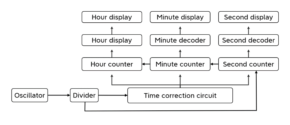
Figure 1. Design schematic (Photo/Picture credit: Original).
2. Relevant Theories
2.1. Oscillator theory
An oscillator is a circuit used to generate a stable AC signal. At its core is a feedback loop that returns a portion of the output signal into the input to maintain oscillation. This feedback circuit also typically includes amplifier elements to provide the required signal gain and ensure that oscillation conditions (Barkhausen stability criterion) are met [3]. The output frequency of an oscillator is determined by the characteristics of its circuit components (such as capacitors, inductors, or quartz crystals) and the feedback loop. According to the required accuracy and frequency range of the usage scenario, select the oscillator type, such as LC oscillator, RC oscillator, crystal oscillator, 555 oscillator, etc.
Among them, the quartz crystal oscillator uses the piezoelectric effect of the quartz crystal to generate oscillation with a stable resonant frequency. When a specific voltage is applied to a quartz crystal, it will produce oscillations at a precise frequency. The 555 oscillator is an integrated circuit based on the 555 timer, which can adjust the oscillator frequency according to external connections and the size of resistors and capacitors. Compared with the quartz crystal oscillator, the frequency accuracy of the 555 oscillator is relatively low, which is affected by external resistance and capacitor resistance, and it is sensitive to temperature. Its oscillation frequency will be affected under different temperature conditions [4].
2.2. Decoding and display theory
The decoding and display process in digital circuits requires the use of a decoder to convert the input digital signal (binary-coded information) into an output signal in order to display or perform specific operations. For example, a 7-segment digital tube decoder converts the digital code into a 7-segment digital tube [5]. input for easy display. LED digital tubes can display information in digital form. When the decoding circuit maps digital signals to these display devices, users can easily read and understand the digital information.
3. Circuit Module Design
3.1. Crystal Oscillator Circuit
On the one hand, a 32768 Hz clock crystal oscillator can be used to connect capacitors and resistors to form a crystal oscillator circuit. The crystal oscillator circuit provides the digital clock with a square wave signal of a stable and accurate frequency of 32768 Hz, which can ensure the accuracy and stability of the digital clock [6].
On the other hand, a 555 timer can also be used to form a multivibrator to generate a pulse signal with a frequency of 1Hz, so that the second pulse signal can be obtained directly without using a frequency dividing circuit, but the time accuracy it generates is not as good as that of a crystal oscillator.
Considering that the second signal pulse is the core module of the digital electronic clock to ensure the timing accuracy of the digital clock, this article uses a 32768 Hz clock crystal oscillator as the pulse source, connects a 10㏁ resistor in parallel, and then connects two 30㎊ capacitors in series to form an oscillation circuit.
3.2. Frequency Divider Circuit
Because the pulse signal generated by the crystal oscillator is a high-frequency square wave signal of 32768 Hz, it needs to be divided 15 times by a frequency dividing circuit to obtain a 1 Hz square wave signal for counting by the second counter. The frequency divider is a counter, which is usually suitable for converting high-frequency input signals into low-frequency output signals [7]. It is generally implemented using a multi-stage binary counter. For example, the frequency division multiple of a 32768 Hz oscillation signal into a 1 Hz square wave signal is 15, that is, the counter that implements this frequency division function is equivalent to a 15-level binary counter. From the perspective of minimizing the number of components, this article chooses multi-pole binary counting circuits CD4060 and 74LS74 to form a frequency-dividing circuit. As shown in Figure 2.
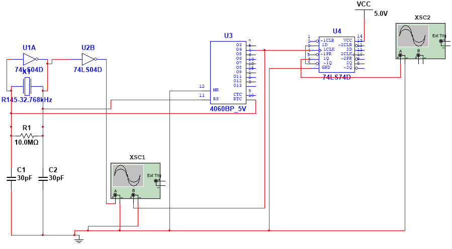
Figure 2. Crystal oscillator and Frequency divider circuit (Photo/Picture credit: Original).
3.3. Decoding Circuit
This article uses CD4511 and a common cathode digital tube to form a decoding display circuit. The CD4511 chip is a BCD code-seven-segment code decoder used to drive a common cathode digital tube display. It has BCD conversion, blanking, and latch control, seven-segment It has decoding and driving functions and can provide large current draw to directly drive LED displays [8].
3.4. Counting Circuit
After the pulse signal passes through the counter, the units and tens digits of “seconds”, “minutes” and “hours” are obtained respectively. The counting of “hours” is a 24-digit number, and the counting of “minutes” and “seconds” is a 60-digit number, and the output is both 8421BCD codes.
There are many ways to implement the counting function: on the one hand, 74LS90 can be used to form a 24-base counting unit and a 60-base counting unit through the feedback-clearing method. Since the 74LS90 is a decimal counter, each counting unit requires two 74LS90 components to function. On the other hand, the 74LS161 counter can be used to form a 24-base counter and a 60-base counter through the feedback setting method. The 74LS390 counter and 74LS08 can also be used to form a counting circuit. 74ls390 is an LSTTL-type dual four-digit decimal counter [9]. The characteristics are that the A and B flip-flops have independent clocks, which can form two divide-by-2 and two divide-by-5 counters. Each counter has a direct clearing, effectively improving system density and buffering the output to reduce the possibility of collector conversion. sex. In view of the simplicity and readability of the circuit, this article selects 74LS90 to form the counting module and uses the feedback clearing method - the NAND gate (74LS00) connects the bits that need to be cleared, and the input signal is re-inputted and output to the clearing terminal (R01 and R02), which can realize the 24-digit counting function. In the same way, the hexadecimal counting function connects the clearing terminal to the high-bit Q1 and Q2 (0101) [10]. When the signal is 6 (0101), the high level of the clearing terminal is cleared. As shown in Figure 3 and 4.

Figure 3. 24-digit counter module (Photo/Picture credit: Original).
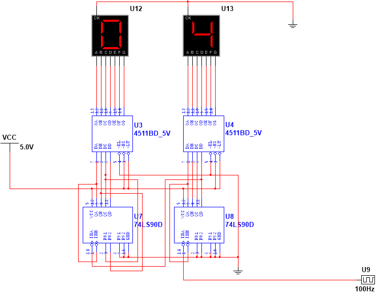
Figure 4. 60-digit counter module (Photo/Picture credit: Original).
3.5. Calibration Circuit
When the digital clock is powered on again or an error occurs in the travel time, the time needs to be manually corrected, that is, a trigger count or a square wave signal with a higher frequency is added to the input end of the counting unit that needs to be corrected. On the one hand, two switches, NAND gate (74LS00) and NOT gate (74LS04) can be used. When the correction switch is closed, by pressing the count plus one button, the count plus one function can be realized for correction; when there is no need to use correction When functioning, turn off the switch and the circuit will time normally. On the other hand, two NAND gates can be used to form an RS flip-flop. During the switch toggle process, the output terminal Q is set to 0 and 1 in sequence, generating a single pulse for counting by the counter, which can achieve bisection or time addition. operation to achieve clock correction. As shown in Figure 5.
Considering the simplicity of the circuit, this article uses the latter, using 74LS00, resistors, and mechanical buttons to form a correction circuit. In order to avoid conflict with its carry signal, this article also uses an AND gate (71LS08) to process the carry signal.
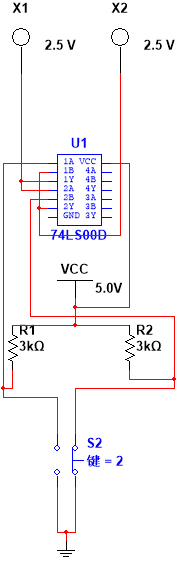
Figure 5. Calibration circuit (Photo/Picture credit: Original).
3.6. Hourly Time Chime Circuit
This article adds an hourly time reporting circuit to the basic timing function. When the time reaches the hour, starting 10 seconds before the hour, the buzzer will sound for 1 second and then 5 times for 1 second. On the one hand, it can be composed of 7 AND gates (two 74LS08 components). When the time is between 59:50 and 00:00, the tens digit of the minute, the unit digits of the minute, and the tens digit of the second remain unchanged, which are 5 (0101), 9 (1001), and 5 (0101) respectively, so the pin corresponding to “1” is connected to the AND gate, thereby generating a time control signal. On the other hand, the eight-input NAND gate 74LS30 can be used to link the unit digits of seconds, tens of seconds, units of minutes, and tens of minutes of the digital electronic clock, and then input in parallel through a NAND gate (74LS00) to achieve NOT gate function, and then connected to the buzzer to tell the time. The two solutions are similar in principle. Since NAND gates are more commonly used in daily logic circuit design, this article adopts the latter.
3.7. Complete Digital Electronic Clock
According to the combination of each module circuit, a complete digital electronic clock simulation diagram is formed as shown in Figure 6.
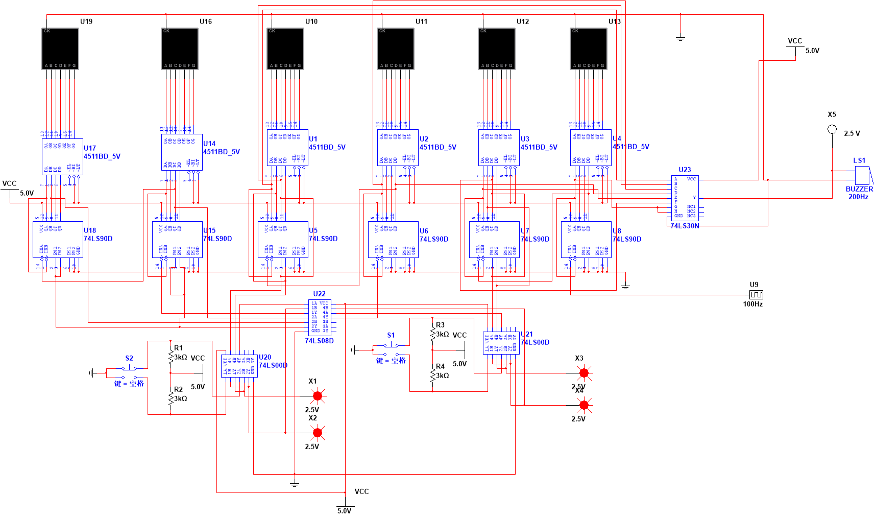
Figure 6. Circuit structure diagram (Photo/Picture credit: Original).
4. Conclusion
The meticulously designed digital electronic clock successfully meets the anticipated outcomes and effectively executes its designated functions. Adopting a top-down design approach, the overarching circuitry is decomposed into discrete, purpose-driven modules. Each module, tailored to cater to specific functionalities, undergoes a rigorous design and debugging process in isolation. Once each individual function achieves optimal performance, the modules are integrated, culminating in a comprehensive debugging session. This systematic and modular approach ensures not only a streamlined design process but also enhances the clock’s efficiency and reliability. By leveraging this method, potential issues inherent within each module can be identified and rectified early on, preventing cascading errors during the final integration. In essence, this approach underscores the importance of methodical planning and iterative testing in the realm of electronic design, ensuring that the final digital electronic clock stands as a testament to precision, functionality, and innovation.
References
[1]. Roy, R., & Kapat, S. (2020). Discrete-time framework for analysis and design of digitally current-mode-controlled intermediate bus architectures for fast transient and stability. IEEE Journal of Emerging and Selected Topics in Power Electronics, 8(4), 3237-3249.
[2]. Lo, S. C., Barker, A. J., Whiteley, S. R., Mlinar, E., Chen, J., Wu, D., & Singhal, K. (2022, April). Simulation methodology for timing analysis and design optimization in digital superconducting electronics. In 2022 23rd International Symposium on Quality Electronic Design (ISQED) (pp. 33-38). IEEE.
[3]. Rao, R. M. S., Asad, M., & Singha, A. K. (2020, December). Analysis and design of a digital average current-mode controlled buck converter. In 2020 IEEE International Conference on Power Electronics, Drives and Energy Systems (PEDES) (pp. 1-4). IEEE.
[4]. Milton, M., De La O, C., Ginn, H. L., & Benigni, A. (2020). Controller-embeddable probabilistic real-time digital twins for power electronic converter diagnostics. IEEE Transactions on Power Electronics, 35(9), 9850-9864.
[5]. Panigrahi, B. K., & Jena, R. K. (2021). Investigate, Analyze, and Design of Real-Time Problems in the Domain of Power Electronics and Energy Using MATLAB: Review and Application. Advances in Energy Technology: Proceedings of ICAET 2020, 235-265.
[6]. Prasad, K. N., & Narayanan, G. (2021). Electromagnetic bearings with power electronic control for high-speed rotating machines: Review, analysis, and design example. IEEE Transactions on Industry Applications, 57(5), 4946-4957.
[7]. Zhu, X., Xu, H., Zhao, Z., & others. (2021). An Environmental Intrusion Detection Technology Based on WiFi. Wireless Personal Communications, 119(2), 1425-1436.
[8]. Tian, Y. (2019, July). The Construction and Development of Digital Electronic Technology Course Majoring in Applied Electronic Technology of Advanced Vocational College. In Proceedings of the 3rd International Conference on Education and Multimedia Technology (pp. 239-244).
[9]. Liao, Y., Wang, X., & Blaabjerg, F. (2020). Passivity-based analysis and design of linear voltage controllers for voltage-source converters. IEEE Open Journal of the Industrial Electronics Society, 1, 114-126.
[10]. Wang, Y., Zhang, J., Guan, Y., & Xu, D. (2022). Analysis and design of a two-phase series capacitor dual-path hybrid DC-DC converter. IEEE Transactions on Power Electronics, 37(8), 9492-9502.
Cite this article
Feng,Z. (2023). Analysis and design research of digital electronic clocks. Theoretical and Natural Science,25,66-72.
Data availability
The datasets used and/or analyzed during the current study will be available from the authors upon reasonable request.
Disclaimer/Publisher's Note
The statements, opinions and data contained in all publications are solely those of the individual author(s) and contributor(s) and not of EWA Publishing and/or the editor(s). EWA Publishing and/or the editor(s) disclaim responsibility for any injury to people or property resulting from any ideas, methods, instructions or products referred to in the content.
About volume
Volume title: Proceedings of the 3rd International Conference on Computing Innovation and Applied Physics
© 2024 by the author(s). Licensee EWA Publishing, Oxford, UK. This article is an open access article distributed under the terms and
conditions of the Creative Commons Attribution (CC BY) license. Authors who
publish this series agree to the following terms:
1. Authors retain copyright and grant the series right of first publication with the work simultaneously licensed under a Creative Commons
Attribution License that allows others to share the work with an acknowledgment of the work's authorship and initial publication in this
series.
2. Authors are able to enter into separate, additional contractual arrangements for the non-exclusive distribution of the series's published
version of the work (e.g., post it to an institutional repository or publish it in a book), with an acknowledgment of its initial
publication in this series.
3. Authors are permitted and encouraged to post their work online (e.g., in institutional repositories or on their website) prior to and
during the submission process, as it can lead to productive exchanges, as well as earlier and greater citation of published work (See
Open access policy for details).
References
[1]. Roy, R., & Kapat, S. (2020). Discrete-time framework for analysis and design of digitally current-mode-controlled intermediate bus architectures for fast transient and stability. IEEE Journal of Emerging and Selected Topics in Power Electronics, 8(4), 3237-3249.
[2]. Lo, S. C., Barker, A. J., Whiteley, S. R., Mlinar, E., Chen, J., Wu, D., & Singhal, K. (2022, April). Simulation methodology for timing analysis and design optimization in digital superconducting electronics. In 2022 23rd International Symposium on Quality Electronic Design (ISQED) (pp. 33-38). IEEE.
[3]. Rao, R. M. S., Asad, M., & Singha, A. K. (2020, December). Analysis and design of a digital average current-mode controlled buck converter. In 2020 IEEE International Conference on Power Electronics, Drives and Energy Systems (PEDES) (pp. 1-4). IEEE.
[4]. Milton, M., De La O, C., Ginn, H. L., & Benigni, A. (2020). Controller-embeddable probabilistic real-time digital twins for power electronic converter diagnostics. IEEE Transactions on Power Electronics, 35(9), 9850-9864.
[5]. Panigrahi, B. K., & Jena, R. K. (2021). Investigate, Analyze, and Design of Real-Time Problems in the Domain of Power Electronics and Energy Using MATLAB: Review and Application. Advances in Energy Technology: Proceedings of ICAET 2020, 235-265.
[6]. Prasad, K. N., & Narayanan, G. (2021). Electromagnetic bearings with power electronic control for high-speed rotating machines: Review, analysis, and design example. IEEE Transactions on Industry Applications, 57(5), 4946-4957.
[7]. Zhu, X., Xu, H., Zhao, Z., & others. (2021). An Environmental Intrusion Detection Technology Based on WiFi. Wireless Personal Communications, 119(2), 1425-1436.
[8]. Tian, Y. (2019, July). The Construction and Development of Digital Electronic Technology Course Majoring in Applied Electronic Technology of Advanced Vocational College. In Proceedings of the 3rd International Conference on Education and Multimedia Technology (pp. 239-244).
[9]. Liao, Y., Wang, X., & Blaabjerg, F. (2020). Passivity-based analysis and design of linear voltage controllers for voltage-source converters. IEEE Open Journal of the Industrial Electronics Society, 1, 114-126.
[10]. Wang, Y., Zhang, J., Guan, Y., & Xu, D. (2022). Analysis and design of a two-phase series capacitor dual-path hybrid DC-DC converter. IEEE Transactions on Power Electronics, 37(8), 9492-9502.