


1. Introduction
The digital electronic clock primarily comprises the digital display, 60-base counter, 24-base counter, frequency oscillator, and timekeeping components. Initially, a stable standard time pulse signal must emanate from a chosen pulse source. In this design, a crystal oscillator serves as the pulse source, providing a time reference signal [1]. The high-frequency pulse signal generated by this source undergoes frequency division to transform it into the second pulse signal required for the experiment (with a frequency of 1Hz). The frequency divider’s output is channeled to the counter for tallying.
Given that both seconds and minutes operate on base 60, and hours on base 24, it becomes imperative to design counters for base 60 and 24 respectively [2]. Each counter’s output signal is relayed to the digital display via the decoder, ensuring digital representation of the “hour”, “minute”, and “second”. In this context, the 74LS90 counting terminal serves as the trigger. Subsequently, the decoding display circuit interprets the status of the “hour”, “minute”, and “second” counters through the seven-segment display decoder, exhibiting it on the six-digit LED seven-segment display. A time correction circuit refines and modifies the real values of “hours”, “minutes”, and “seconds”. Furthermore, the design incorporates an hourly chime feature. Beginning 10 seconds prior to the hour, a buzzer chimes five times, each for 1 second, followed by a 1-second pause. To ensure manual adjustments to hours and minutes, another time correction circuit becomes necessary. This circuit refines and modifies the displayed values of “hours”, “minutes”, and “seconds”.
2. Overall Design Scheme
2.1. Design Ideas
Digital electronic clocks adopt the development of digital integrated circuits and advanced quartz technology, which make electronic clocks have the advantages of accurate time, stable performance, and easy portability. Electronic clocks are automatically used in timing [3]. There are good developments and applications in various fields such as alarms, automatic ringing on time, automatic time program control, scheduled broadcast, and automatic control. The development of integrated circuits and the widespread use of quartz crystal oscillators have made electronic clocks far more accurate than old-fashioned clocks. The digitization of clocks has brought great convenience to people’s production and life and has greatly expanded the original time-telling functions of clocks. Therefore, it is of very practical significance for this newspaper to realize digital clocks and expand their applications through logic chips [4].
This circuit design uses a logic chip to implement a digital clock. Quartz crystal is used to form a pulse signal, and the second pulse signal is counted and reset through a counting circuit, corresponding to hours, minutes, and seconds respectively, and then connected to the digital tube through a decoding circuit to achieve the display function. It also has manual time correction and minute correction functions. Hourly time chime function [5].
2.2. Design Schematic Diagram
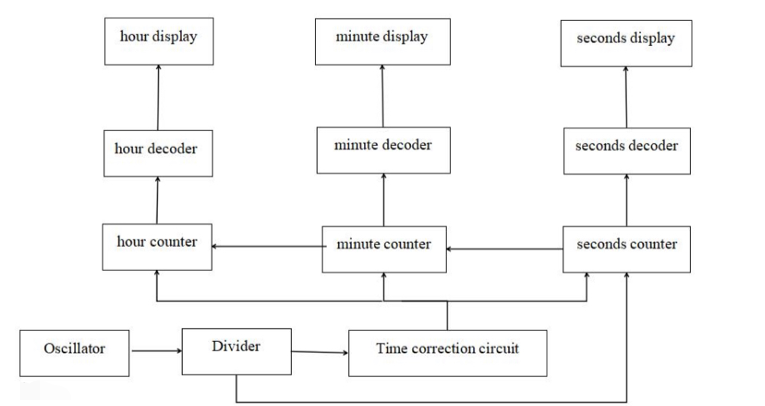
Figure 1. Design schematic (Photo/Picture credit: Original).
The schematic design can be visualized in Figure 1, as illustrated below. This diagram provides a detailed representation of the design’s architecture and its interconnected components.
3. Introduction to the Functions of Each Module
3.1. Body Oscillation Circuit
The crystal oscillator circuit is composed of a crystal oscillator 32768Hz and a capacitor to the digital electronic clock. It provides a square wave signal with a stable and accurate frequency of 32768Hz, which can ensure the accuracy and stability of the digital electronic clock [6]. Whether it is an analog electronic clock or a digital display electronic clock, a crystal oscillator circuit is used.
3.2. Frequency Divider Circuit
The frequency divider circuit divides the 32768HZ high- frequency square wave signal 15 times to obtain a 1Hz square wave signal for the second counter to count. The frequency divider is actually a counter [7].
3.3. Counting Circuit
The counting circuit is composed of second units and seconds counters, minute units, and minute tens counters, timely ones and hour tens counter circuits, in which the second units and seconds counters, minute units and minute tens counters are. It is a 60-digit counter, and according to the design requirements, the hour ones and tens counters are 24- digit counters [8].
3.4. Decoding Circuit
The decoding drive circuit converts the 8421BCD code output by the counter into the logic state required by the digital tube and provides sufficient operating current to ensure the normal operation of the digital tube.
3.5. Calibration Circuit
When the power is turned on again or there is an error in the trend, the circuit must be calibrated [9]. Usually, calibration requires cutting off the direct counting path during division and summing, adding a higher frequency signal source, or performing manual trigger counting to achieve the correction function.
3.6. Hourly Time Circuit
When the time of the digital electronic clock reaches 10 seconds before the hour, the buzzer will sound 5 times for 1 second and then for 1 second.
4. Design of Each Module of the Circuit
4.1. Oscillation Circuit
Option 1: Use a crystal oscillator of 32768Hz connected to a capacitor and a resistor to form a crystal oscillation circuit. The crystal oscillator circuit provides the digital clock with a square wave signal of a stable and accurate frequency of 32768Hz, which can ensure the accuracy and stability of the digital clock.
Option 2: Use a 555 timer to form a multivibrator circuit. The period is 1Hz, so there is no need to use a frequency dividing circuit and the second pulse signal can be obtained directly, but the time accuracy is not as good as the crystal oscillator.
1. Because the second signal pulse is the core part of the digital electronic clock, it requires high accuracy to achieve. Therefore, this design uses option one. Although it requires adding a frequency division circuit compared to option two, the accuracy is accurate, and option two may have unstable clock signals, so option one is better [10].
The module is realized by connecting a crystal oscillator in parallel with a resistor and then connecting two capacitors in series. According to the equipment provided in the experiment, the resistance value is selected to be 20MΩ and the capacitance value is 30pF. The simulation circuit diagram is shown in Figure 2.
4.2. Frequency Division Circuit
The frequency divider circuit divides the 32768Hz high-frequency square wave signal 15 times to obtain a 1Hz square wave signal for the second counter to count. The frequency divider is a counter. Usually, the output frequency of the crystal oscillator of a digital clock is relatively high. To obtain a 1Hz second signal input, the output signal of the oscillator needs to be frequency-divided. Usually, the circuit that implements the frequency divider is a counter circuit, which is generally implemented using a multi-stage binary counter. For example, the frequency division multiple of 32768Hz oscillation signal to 1Hz is 15, that is, the counter that implements the frequency division function is equivalent to a 15-level binary counter. From the perspective of minimizing the number of components, multi-pole binary counting circuits CD4060 and CD4040 can be selected to form a frequency-dividing circuit. CD4060 and CD4040 have the highest number of frequency divisions among digital integrated circuits, and CD4060 also contains the NOT gate required for the oscillation circuit, making it more convenient to use.
Option 1: Use CD4060 as the main component of the frequency division circuit. Because the pulse signal is provided by a crystal oscillator circuit, the generated frequency is f=215Hz=32768Hz. The frequency generated by the quartz crystal frequency is divided by 214 times CD4060 to obtain a frequency of 2Hz, and the frequency of 2Hz is divided by a 74LS74 to obtain a frequency of 1Hz.
Option 2: The clock signal can also be divided by using the CD4040 counter. The counting modulus of the CD4040 counter is 4096. If the 32768 Hz signal is divided into 1 Hz, an additional 8-divider counter is needed to achieve the 15-level frequency division required by the design. Not commonly used in general experiments.
To sum up, this study chooses the CD4060 of option 1 to form a frequency dividing circuit, as Fig 2 exhibit. By connecting a 74LS74 in series, 15 levels of 2-frequency division can be achieved, and a 1Hz signal can be obtained, so the first option is more reasonable.
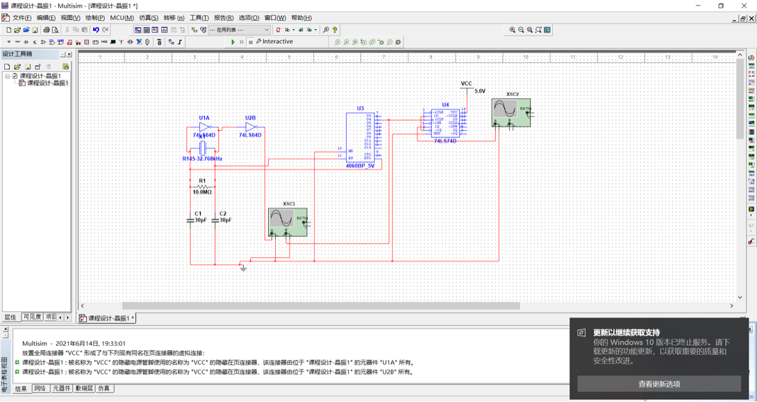
Figure 2. Crystal oscillator and Frequency divider circuit (Photo/Picture credit: Original).
4.3. Counting Circuit
After the signal passes through the counter, the units and tens digits of “seconds”, the units and tens of “minutes” and the units and tens of “hours” are obtained respectively. The counting of “hours” is a 24-digit number, the counting of “minutes” and “seconds” is a sexagesimal number, and the output is both 8421BCD codes.
Solution 1: Use 74LS90 to form a 24-base counting unit and a 60-base counting unit through feedback feedback-clearing method. Due to the characteristics of 74LS90 itself, each unit requires two 74LS90 components to realize its function.
Solution 2: Use the 74LS161 counter to form a 24-base counter and a 60-base counter through the feedback setting method. 74LS161 is a commonly used four-digit binary presettable synchronous adding counter. It can be flexibly used in various digital circuits and microcontroller systems to implement many important functions such as frequency dividers.
Option 3: Use the 74LS390 counter and 74LS08 to form a counting circuit. 74ls390 is an LSTTL-type dual four-digit decimal counter. The characteristics are that the A and B flip-flops have independent clocks, which can form two divide-by-2 and two divide-by-5 counters. Each counter has a direct clearing, effectively improving system density and buffering the output to reduce the possibility of collector conversion. sex.
The above three methods are all relatively effective. Considering the limitations of economy and laboratory conditions, the optimal solution for this design is Option 1, so Option 1 is used for the design.
Using the feedback clearing method, use a NAND gate (74LS00) to connect the bits that need to be cleared input the primary input signal again, and then output it to the R01 and 2 clearing terminals to achieve the 24-digit counting function. In the same way, for the hexadecimal counting function, the clearing terminal is connected to the high-order Q1 and Q2 (signal 0101). When the signal is 6 (0101), the clearing terminal is cleared to a high level. As shown in Figure 3 and 4.
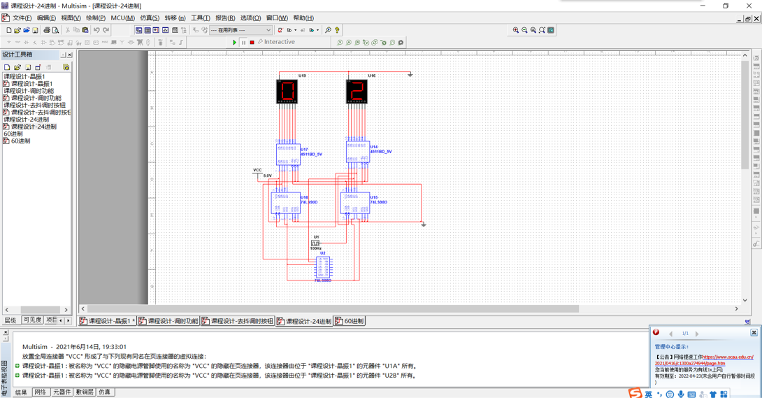
Figure 3. 24-digit counter module (Photo/Picture credit: Original).
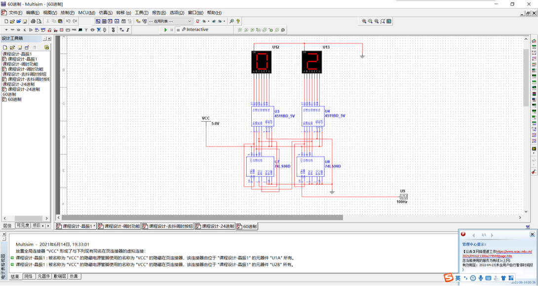
Figure 4. 60-digit counter module (Photo/Picture credit: Original).
4.4. Decoding Display Circuit
Decode the 8421BCD code output by the counter and display it through the digital tube.
CD4511 and common cathode digital tube are used to form a decoding display circuit, CD4511 decoder and common cathode digital tube. CD4511 is a BCD code-seven-segment code decoder used to drive a common cathode digital tube display. CMOS circuits with BCD conversion, blanking and latch control, seven-segment decoding and driving functions can provide larger source current. It can directly drive LED displays. As shown in Figure 5.
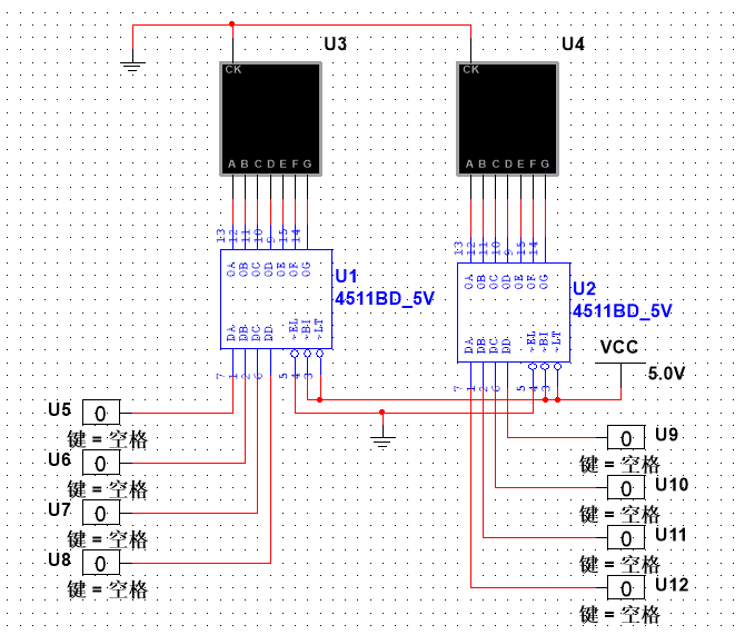
Figure 5. Decoding display circuit module (Photo/Picture credit: Original).
4.5. Correction Circuit (Anti-Shake Circuit)
The time needs to be corrected when the power is turned on again or when an error occurs. Usually, the method of correcting the time is: first cut off the normal counting path, and then perform manual trigger counting or add a higher frequency square wave signal to the input end of the counting unit that needs to be corrected. After correction, switching to normal Timing status is enough.
Option 1: Use two switches, a NAND gate (74LS00) and a NOT gate (74LS04). When the calibration switch is closed, by pressing the count plus one button, the count plus one function can be realized to achieve correction, when there is no need to use calibrating the function, turn off the switch to achieve normal carry.
Option 2: Use two NAND gates to form an RS flip-flop. When the switch is flipped left and right, the output terminal Q is set to 0 and 1 in sequence, generating a single pulse for counting by the counter, which can realize bisection or time addition. One operation to achieve calibration.
Option 3: Use switches and NAND gates to form a control circuit. When the switch is turned on, the normal input signal can pass smoothly, so the time correction circuit is in the normal timing state; when the switch is turned to one end, the signal generation time correction circuit is in the time correction state.
In summary, the three options are all feasible from the perspective of use. Taking into account the limitations of the economy and laboratory conditions, the second option with the fewest components is selected for design. In order to avoid conflict with its carry signal, this experiment also used an AND gate (71LS08) to process the carry signal. As shown in Figure 6.
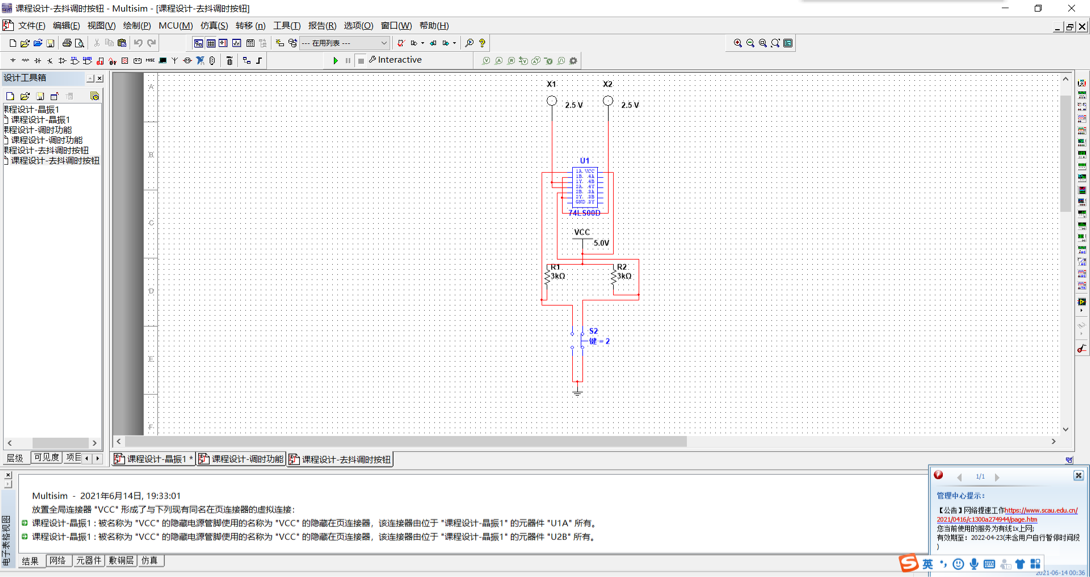
Figure 6. Calibration circuit (Photo/Picture credit: Original).
4.6. Whole, Point Time Circuit
The requirements of this design are that when the time reaches the hour, starting 10 seconds before the hour, the buzzer will sound 5 times for 1 second, then stop for 1 second.
Option 1: Use 7 AND gates (two 74LS08 components). When the time ranges from 59 minutes and 50 seconds to 00 minutes and 00 seconds, the minute tens digit, minute ones digit, and second tens digit remain unchanged, which are 5, 9, and 5 respectively. Therefore, the Qc and Qa of the tens digit of the minute counter can be changed, Qd and Qa of the unit digit, Qc and Qa of the tens digit of the seconds counter, and Qa of the unit digit of the seconds counter are phased together to generate a timekeeping control signal.
Option 2: Use the eight-input NAND gate 74LS30 to link the second digit, the second tens digit, minute ones, and minute tens digits of the digital electronic clock, and then input it in parallel through a NAND gate (74LS00) (to realize the NOT gate function). Connect to a buzzer to tell time.
Option 3: It is composed of 7 NAND gates (two 74LS00 components) and one NOT gate (74LS04 component). The composition method and principle are roughly the same as Option 1.
In summary, the three options are all feasible from the perspective of use. Considering the limitations of the economy and laboratory conditions, option 2 was selected for this design. As shown in Figure 7.
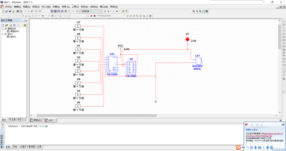
Figure 7. Hourly time chime circuit (Photo/Picture credit: Original).
4.7. Complete Digital Electronic Clock
According to the combination of each module circuit, a complete digital electronic clock simulation diagram is formed as shown in Figure 8.
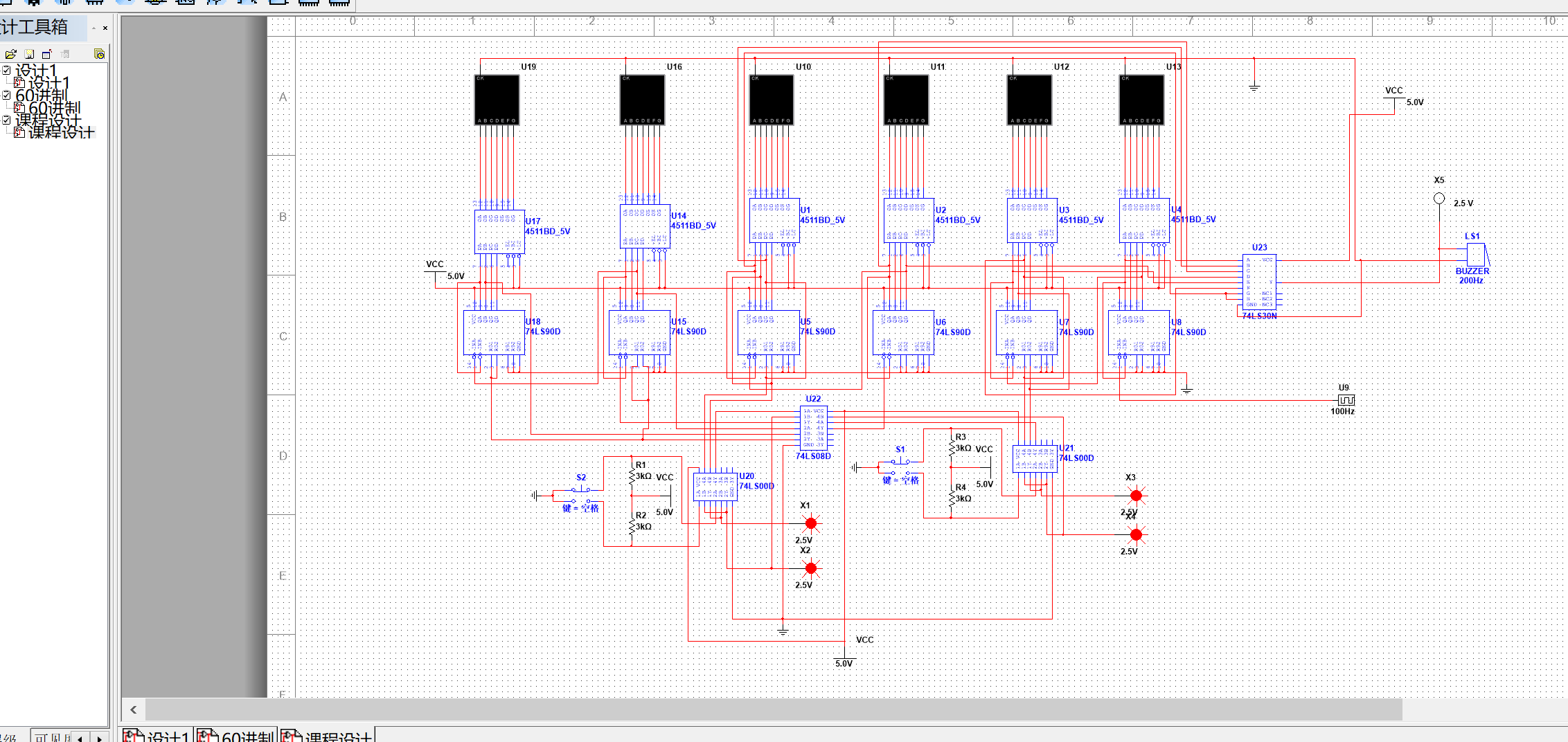
Figure 8. Complete circuit (Photo/Picture credit: Original).
According to the above circuit diagram design, the physical electronic clock (Figure.9) can also be made by soldering a breadboard and the required chip.
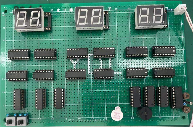
Figure 9. Physical electronic clock (Photo/Picture credit: Original).
5. Conclusion
The conceived digital electronic clock effectively meets its intended objectives and embodies the desired features. Utilizing a top-down design approach, the comprehensive circuitry is segmented into distinct functional modules. Each of these modules is tailored to cater to specific functionalities. Following the meticulous design phase, every module undergoes rigorous testing and debugging. Ensuring the flawless operation of each individual module is paramount before initiating their integration. This systematic integration and subsequent end-to-end debugging culminate in the successful realization of a sophisticated digital electronic clock. Through such a structured approach, not only is the robustness of the clock ensured, but its adaptability and scalability for future enhancements are also solidified. This method underscores the importance of modular design and iterative testing in the creation of advanced electronic devices.
References
[1]. Hudgikar, S. R. K. (2022). A study on design and construction of a digital clock system. International Journal of Research and Analysis in Science and Engineering, 2 (2), 8-8.
[2]. Akanni, J., Abdulrasaq, A., Isa, A. A., & Ojo, A. O. (2022). Development of a Compact and Accurate Auto-Update Digital Clock with Real-Time Location Display using Organic Light Emitting Diode and Crystal Oscillator. Journal of Applied Sciences and Environmental Management, 26 (8), 1391-1396.
[3]. Khan, M. M., Tasneem, N., & Marzan, Y. (2021, January). ‘Fastest Finger First-Educational Quiz Buzzer’Using Arduino and Seven Segment Display for Easier Detection of Participants. In 2021 IEEE 11th Annual Computing and Communication Workshop and Conference (CCWC) (pp. 1093-1098). IEEE.
[4]. Devi, D. A., & Rani, N. S. (2019, January). Design and implementation of custom IP for real time clock on reconfigurable device. In 2019 Third International Conference on Inventive Systems and Control (ICISC) (pp. 414-418). IEEE.
[5]. Zhu, X., Xu, H., Zhao, Z., & others. (2021). An Environmental Intrusion Detection Technology Based on WiFi. Wireless Personal Communications, 119 (2), 1425-1436.
[6]. Manik, A. T. (2020). Design of a Digital Clock Application Using the Atmega 8535 Microcontroller Based Alarm. Instal: Jurnal Komputer, 12(01), 30-35.
[7]. Badiganti, P. K., Peddirsi, S., Rupesh, A. T. J., & Tripathi, S. L. (2022). Design and Implementation of Smart Healthcare Monitoring System Using FPGA. In Proceedings of First International Conference on Computational Electronics for Wireless Communications: ICCWC 2021 (pp. 205-213). Springer Singapore.
[8]. Gadde, G. R., & Kiran, V. Optimization of Area, Power, and Delay in BCD to Seven segment decoder using MGDI Technique.
[9]. Rawf, K. M. H., & Abdulrahman, A. O. (2022). Microcontroller-Based Kurdish Understandable and Readable Digital Smart Clock. Science Journal of University of Zakho, 10 (1), 1-4.
[10]. Owen-Block, B. J. (2023). Mechanical Seven-Segment Display Clock (Doctoral dissertation, Massachusetts Institute of Technology).
Cite this article
Cheng,Z. (2023). Design and implementation of a digital clock using a seven-segment display. Theoretical and Natural Science,14,224-232.
Data availability
The datasets used and/or analyzed during the current study will be available from the authors upon reasonable request.
Disclaimer/Publisher's Note
The statements, opinions and data contained in all publications are solely those of the individual author(s) and contributor(s) and not of EWA Publishing and/or the editor(s). EWA Publishing and/or the editor(s) disclaim responsibility for any injury to people or property resulting from any ideas, methods, instructions or products referred to in the content.
About volume
Volume title: Proceedings of the 3rd International Conference on Computing Innovation and Applied Physics
© 2024 by the author(s). Licensee EWA Publishing, Oxford, UK. This article is an open access article distributed under the terms and
conditions of the Creative Commons Attribution (CC BY) license. Authors who
publish this series agree to the following terms:
1. Authors retain copyright and grant the series right of first publication with the work simultaneously licensed under a Creative Commons
Attribution License that allows others to share the work with an acknowledgment of the work's authorship and initial publication in this
series.
2. Authors are able to enter into separate, additional contractual arrangements for the non-exclusive distribution of the series's published
version of the work (e.g., post it to an institutional repository or publish it in a book), with an acknowledgment of its initial
publication in this series.
3. Authors are permitted and encouraged to post their work online (e.g., in institutional repositories or on their website) prior to and
during the submission process, as it can lead to productive exchanges, as well as earlier and greater citation of published work (See
Open access policy for details).
References
[1]. Hudgikar, S. R. K. (2022). A study on design and construction of a digital clock system. International Journal of Research and Analysis in Science and Engineering, 2 (2), 8-8.
[2]. Akanni, J., Abdulrasaq, A., Isa, A. A., & Ojo, A. O. (2022). Development of a Compact and Accurate Auto-Update Digital Clock with Real-Time Location Display using Organic Light Emitting Diode and Crystal Oscillator. Journal of Applied Sciences and Environmental Management, 26 (8), 1391-1396.
[3]. Khan, M. M., Tasneem, N., & Marzan, Y. (2021, January). ‘Fastest Finger First-Educational Quiz Buzzer’Using Arduino and Seven Segment Display for Easier Detection of Participants. In 2021 IEEE 11th Annual Computing and Communication Workshop and Conference (CCWC) (pp. 1093-1098). IEEE.
[4]. Devi, D. A., & Rani, N. S. (2019, January). Design and implementation of custom IP for real time clock on reconfigurable device. In 2019 Third International Conference on Inventive Systems and Control (ICISC) (pp. 414-418). IEEE.
[5]. Zhu, X., Xu, H., Zhao, Z., & others. (2021). An Environmental Intrusion Detection Technology Based on WiFi. Wireless Personal Communications, 119 (2), 1425-1436.
[6]. Manik, A. T. (2020). Design of a Digital Clock Application Using the Atmega 8535 Microcontroller Based Alarm. Instal: Jurnal Komputer, 12(01), 30-35.
[7]. Badiganti, P. K., Peddirsi, S., Rupesh, A. T. J., & Tripathi, S. L. (2022). Design and Implementation of Smart Healthcare Monitoring System Using FPGA. In Proceedings of First International Conference on Computational Electronics for Wireless Communications: ICCWC 2021 (pp. 205-213). Springer Singapore.
[8]. Gadde, G. R., & Kiran, V. Optimization of Area, Power, and Delay in BCD to Seven segment decoder using MGDI Technique.
[9]. Rawf, K. M. H., & Abdulrahman, A. O. (2022). Microcontroller-Based Kurdish Understandable and Readable Digital Smart Clock. Science Journal of University of Zakho, 10 (1), 1-4.
[10]. Owen-Block, B. J. (2023). Mechanical Seven-Segment Display Clock (Doctoral dissertation, Massachusetts Institute of Technology).