


1. Introduction
Since the late 1900s, integrated circuit technology has emerged and evolved significantly. Moore's law, proposed by Gordon Moore in 1969, suggests that the number of transistors on a chip would double approximately every two years [1]. This observation underscores the trajectories and principles guiding IC technology advancements. The burgeoning growth of computers and mobile phones heightens the demand for more compact, powerful, and efficient chips. As a result, numerous innovations in IC technology have been introduced over the decades. Notably, material enhancements in CMOS have been realized, with high-k dielectric materials replacing the traditional SiO2 layer to diminish leakage current [2]. Additionally, the FinFET has enhanced scaling performance by transitioning from a planar structure to a 3-D design, significantly improving gate control. Concurrently, technologies like CNTFET, which integrate structural and material enhancements, are being introduced. CNTFET represents an avant-garde design utilizing carbon nanotubes through its gate, drain, and source. Yet, these technological advancements introduce challenges, especially in the fabrication process and control design.
This manuscript aims to elucidate advanced IC technology, with a particular focus on CMOS, FinFET, and CNTFET. Their distinct characteristics will be explored, comparing their strengths and weaknesses, to discern their potential application in contemporary IC circuit design. Following this, a simulation of CMOS and FinFET NAND gates will be presented, illustrating specific features and suggesting avenues for future research.
2. Field Effect Transistors and Their Characteristics
2.1. CMOS
Firstly, the CMOS technology will be introduced in this section. CMOS consists of PMOS and NMOS as figure 1 shown below and it is widely used in integrated circuit technology. It is also one of the dominant technologies in integrated circuit design.
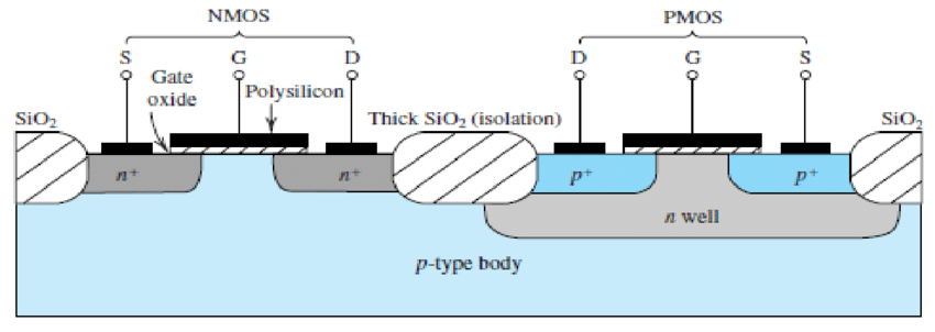
Figure1. Cross-section structure of CMOS [3].
Compared with the former IC technology TTL (Transistor-Transistor logic), the CMOS has many advantages that makes it outstanding in application. Firstly, the power consumption of CMOS is much lower than the former technology. Different form TTL which is current driven gate, CMOS is voltage controlled gate. Its low power dissipation can avoid self-heating problems which is of great importance in complex logic ICs. Secondly, the noise margin of the CMOS is higher than TTL. According to Chen and Touba (2009), under 5V condition, the CMOS noise margin high ( \( N{M_{H}}) \) is 0.96V and noise margin low ( \( N{M_{L}}) \) is 1V. However, the TTL \( N{M_{H}} \) is 0.4V and \( N{M_{L}} \) is 0.4V [4]. It is obvious that the noise margin of CMOS is much higher than TTL which means it has higher immunity to voltage fluctuations and unexpected noises.
In regards of the switching speed of CMOS, CMOS has slower switching speed historically than TTL. However, with the development of the CMOS technology, the High-speed CMOS technique has been applied in IC design and it can achieve giga-bit/s in actual application [5]. It is the same case in propagation delay of CMOS which is decided by the switching characteristics.
According to the Moore’s law, the CMOS technology has been scaling down over the years according to the graph shown below. At the same time, the performance of the CMOS also optimized over the years, including power loss, noise margin, switching speed, parasitic capacitance and power density etc. However, the traditional CMOS technology has been limited to 20nm because of the Quantum effect [6]. Thus, more advanced technology like FinFET, GAAFET, CNTFET have been researched and designed recent years. And they improve both the structure and material of the device.
2.2. FinFET
Due to the size restriction of the traditional CMOS technology, FINFET has been developed these years to both scale down the size and improve the performance. Compared with traditional MOS, FinFET uses a 3D structure that warps around the three sides of the channel (fin) of the FinFET as the picture shown Figure 2:
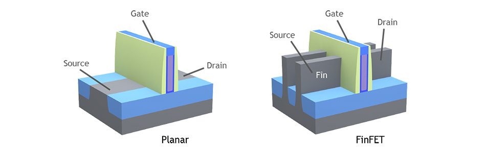
Figure 2. Comparison between Planar MOS and FinFET [7].
Unlike the Planar MOS which the gate only sits on the top of the drain-source channel, the FinFET has more contact area between gate and channel. As a result, is leads to the great improvement of the electrostatics of the FinFET [8], which means the channel can be better controlled. Moreover, the leakage current also has been largely reduced due to this characteristic.
Due to the improvement of the electrostatics, FinFET has many advantages over traditional MOSFET. Firstly, it makes the further scaling of the transistor possible. FinFET can further reduce the gate length ( \( {L_{gate}}) \) as the figure 3 shown:
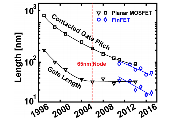
Figure 3. Comparison of \( {L_{gate}} \) Scaling trend between Planar MOSFET and FinFET [9].
It is obvious that the FinFET can be fabricated to a smaller size and it can pack more transistors in one chip. Secondly, the on and off current ratio of the FinFET has been greatly improved, and it indicates a lower static power consumption when FinFET is at off state. Moreover, the subthreshold swing of has been largely reduced too, which means both improvement in performance and active power consumption. Another important improvement of FinFET is the switching speed of the device. According to the study, the switching speed has been reduced to a few picoseconds [10]. And it reveals FinFET’s ability to work under high-speed digital logic application.
However, there are also limitations in FinFET. The first problem is the fabrication of the devices. Its 3D structure makes it more complex and harder to manufacture, including the control of height and width of thin fins, gate structures and removal of corner residue. Thus, it increases the cost of the device. Moreover, the increasing transistor density also brings the challenge in power distribution and controlling. More complex and dedicated control system should be designed to obtain better power distribution and thermal control.
2.3. CNTFET
After the widely use of FinFET, CNTFET is one of the most updated technologies in integrated circuit design and its full name is Carbon Nano-Tube Field Effect Transistor. Unlike MOSFET and FinFET, it hasn’t been widely put into commercial use currently, because of its cost and fabrication challenge. The main difference between CNTFET and FinFET is the material of the channel. The conventional silicon channel material has been replaced by numbers of carbon nanotubes as shown in Figure 4:
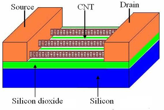
Figure 4. General structure for CNTFET [11].
It is clear that the CNT channel in CNTFET is warped with a graphite sheet called SWCNT [12]. And it has extremely strong physical structure. Due to its material innovation, CNTFET is expected to open a new era because of its excellent electrical and structural performance.
Firstly, CNTFET overcomes the heat dissipation problem compared with FinFET, which may easily get heat accumulated on the fins [13]. The deliciated carbon nanotube structure in CNT channel has the advantage of low self-heating effect and thermal noise, which leads to the great heat dissipation in CNTFET [14]. Moreover, the carbon channel in CNTFET is undoped while the source and drain are heavily doped, which means that the off-power loss (leakage current) will be largely reduced [15]. And it makes CNTFET a great option in low power high performance design.
More importantly, according to the experiment and research, the switching speed of CNTFET is hundreds of times faster than the planer MOSFET and 3 times faster than FinFET when they are supplied with the same power. Thus, CNTFET can work under extremely high frequency and will be a promising choice in next generation VLSI design.
2.4. Summary and Discussion
To be concluded, with the development of the IC technology, the performance and density of the transistor rapidly improved within the decades. The main characteristics of the transistor are the scaling, switching speed, propagation delay, noise immunity power and heat dissipation. These are the essential elements when evaluating transistors performance, and the latest technology always outperforms the older ones. Moreover, nowadays, the main exploring areas if transistors are the innovation in the structure FinFET and material, while the fabrication challenge and cost become larger.
3. Simulation of CMOS and FinFET Technologies Based on Logic Gates
3.1. Logic Gate Building and Simulation Settings
In this section, the simulation of the traditional planar CMOS and FinFET will be conducted. The aim of the simulation is to use CMOS and FINFET to build a logic NAND gate. Then, different characteristics of the technology will be simulated and analyzed under this NAND gate configuration. The models used in the simulation are form predictive technology model which provides the tools for device modeling of advanced IC technology. In the CMOS simulation, models with different scales are applied: (0.8um CMOS, 0.35um CMOS, 180nm CMOS), and all the CMOS circuit are bulit and simulated in LTspice. While the FinFET is 7nm technology, and simulated in Hspice with netlist file.
After the building of the NAND gate, three different characteristics of the device: switching speed, propagation delay and noise margin of the NAND gates will be analyzed and compared to verify the characteristic discussed above. The simulation circuits built for CMOS in LTspice and FINFET in Hspice as shown in Figure 5:
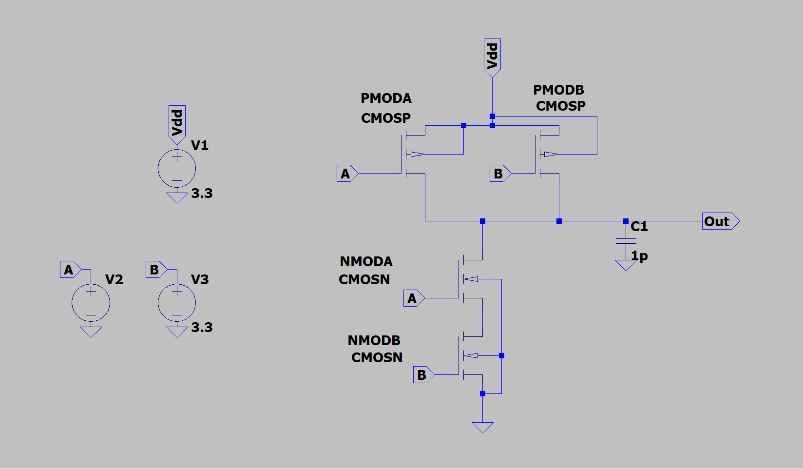
Figure 5. Building of NAND gate in different technologies (Photo/Picture credit: Original).
3.2. Simulation Results and Discussion
3.2.1. Switching speed. Firstly, the switching speed simulation will be presented in this section. When conducting the simulation, \( {V_{dd}} \) and \( {V_{b}} \) is set to 5V and the input of \( {V_{a}} \) is set as a 0.5MHz pulse with 5V peak and 10ns rising and falling edge. Thus, it represents the condition when input AB changes from 01 to 11 and vice versa. In CMOS simulation, the width of length ratio (W/L) is set to 4 in PMOS and 2 in NMOS. However, due to the scaling and modelling difference in FinFET, the input voltage limit is set to 1V in both power supply and signal.
During the simulation, the switching speed of the gate is defined as the time when the voltage between 10% and 90%. Part of the simulation outcome graphs and complete simulation results as shown in Figure 6:
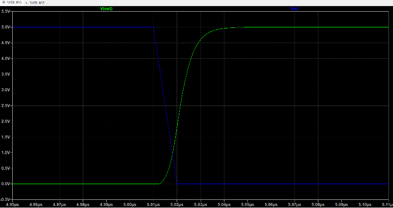
(a) 0.35um cmos on tran.
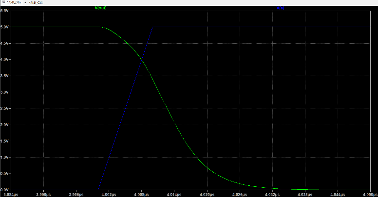
(b) 0.35um cmos off tran.
Figure 6. ON and OFF character of the 0.35um cmos gate (Photo/Picture credit: Original).
Table 1. Switching speeds for different technologies.
0.8um CMOS | 0.35um CMOS | 180nm CMOS | 7NM FINFET | |
On speed | 26ns | 12ns | 8ns | 2.5ns |
Off speed | 29ns | 16ns | 15ns | 2.4ns |
From the table 1 it is clear that the FINFET switching speed is much faster than all the scale of CMOS technology, which matches the expectations. Moreover, within the CMOS technology, with the scaling of the CMOS, the switching speed tends to be faster. At the same time, specific design of the CMOS and FinFET gate also influence its on and off characteristics, such as width and length ratio of the CMOS device, and fin numbers of the FinFET device.
Moreover, there are also other factors that may influence the switching speed of the system:
a). power supply and gate voltage.
b). the slew rate of the input pulse (10ns in the simulation).
c). different combination of input (AB= 00, 01, 11, 10).
These different characteristics can be analysed in the future research.
3.2.2. Propagation delay. In this section, the propagation delay of the NAND gate will be simulated and analysed. The simulation setting for the propagation delay is the same as the switching speed. Under these settings, the propagation delay can be considered as the time difference between the input and output switching point, which equals to 0.5 \( {V_{dd}} \) . the delay is divided into two parts: low to high delay ( \( {t_{pHL}} \) )and high to low delay ( \( {t_{pLH}} \) ), and the average propagation delay can be measured with the equation below:
\( {t_{P}}=\frac{{t_{pHL}}+{t_{pLH}}}{2}\ \ \ (1) \)
Thus, the results of the propagation delay is shown in table 2:
Table 2. Propagation delay for different technologies.
0.8um CMOS | 0.35um CMOS | 180nm CMOS | 7NM FINFET | |
\( {t_{pHL}} \) | 29ns | 15ns | 8ns | 0.2ns |
\( {t_{pLH}} \) | 11ns | 11ns | 7ns | 0.2ns |
\( {t_{P}} \) | 20ns | 13ns | 7.8ns | 0.2ns |
From the table, it is noticeable that the FinFET almost has no propagation delay, and all the CMOS delay is within 20ns. It is similar to the simulation results in switching speed. Moreover, smaller CMOS technology tends to have shorter propagation delay, which indicates the improvement in performance.
Furthermore, other factors that will influence the behavior of the propagation delay are similar to the areas mentioned in switching speed. And they can be further investigated in the future.
3.2.3. Noise margin. In the third section, the DC analysis of the NAND gate will be conducted and the result will be utilized to calculate the noise margin of different design. Noise margin reflects the tolerance of noise like voltage fluctuations, Electromagnetic Interference for the device or the system. Larger noise margin means that the device is more robust to the noise. The noise margin can be illustrated as the graph shown below:
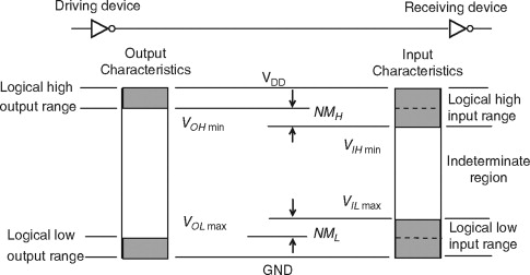
Figure 7. Noise margin explanations [16].
In the figure 7, the noise margin is divided into 2 parts: Noise margin high ( \( {NM_{H}} \) ) and Noise margin low ( \( {NM_{L}} \) ). Moreover, these two elements can be calculated with two equations shown below:
\( {NM_{H}}={V_{OH}}-{V_{IH}} \)
\( {NM_{L}}={V_{IL}}-{V_{OL}} \)
In order to get the noise margin parameters, the DC analysis simulation should be conducted to get the transfer function of the NAND gate. In the simulation, the CMOS DC voltage sweeps from 0 to 5V at input A and the input B is fixed at 5 V, which simulates the condition when AB changes from 01 to 11. The voltage used in FinFET simulation is 1V. Thus, the CMOS simulation under 1 V condition also conducted to get a comprehensive analysis. After getting the transfer function of the device, \( {V_{OH}},{ V_{IH}}{, V_{IL}}, {V_{OL}} \) can be obtained through the points where the function’s gradient equals to -1, as the figures 8 shown below:
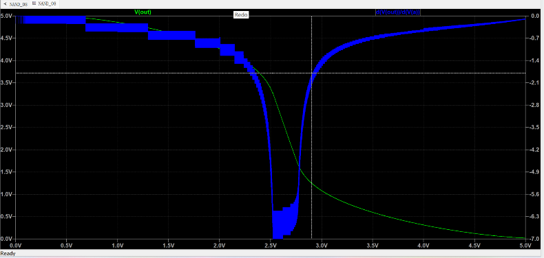
(a) 0.8um CMOS transfer function
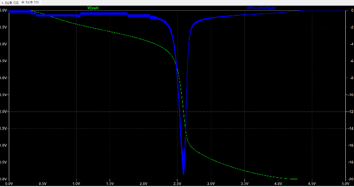
(b) 0.35um CMOS transfer function
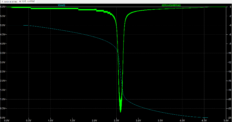
(c) 180nm CMOS transfer function
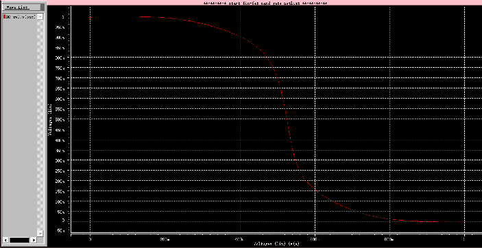
(d) 7nm FinFET transfer function
Figure 8. DC transfer of different technology (Photo/Picture credit: Original).
It is clear that the convex like bond line with negative peak illustrated in the graph is the gradient of the transfer function which helps to find the -1 point. After that, the results can be calculated through the equation shown above, and table 3 contains all the simulation results:
Table 3. Simulation results for noise margin.
0.8um CMOS (5V) | 0.35um CMOS (5V) | 180nm CMOS (5V) | 180nm CMOS (1V) | 7NM FINFET (1V) | |
\( {V_{IL}} \) | 2.08V | 2.26V | 2.28V | 444mV | 413mV |
\( {V_{IH}} \) | 3.2V | 2.94V | 2.95V | 519mV | 643mV |
\( {V_{OH}} \) | 4.14V | 3.93V | 4.125V | 975mV | 889mV |
\( {V_{OL}} \) | 0.8V | 0.625V | 0.678V | 220mV | 104mV |
\( {NM_{L}} \) | 1.28V | 1.635V | 1.602V | 224mV | 309mV |
\( {NM_{H}} \) | 0.94V | 0.99V | 1.175V | 456mV | 246mV |
From the table, it is noticeable that with the scaling of CMOS technology, the CMOS noise margin becomes larger. This indicates that the CMOS becomes more immune to the noise. When comparing the noise margin or 7nm FinFET and 180nm CMOS under 1V condition, \( {NM_{L}} \) of FinFET is larger than 180nm CMOS, while \( {NM_{H}} \) is smaller. This result seems to be controversial, which can be further explored in the future. However, it can be generally concluded that the FinFET outperforms CMOS in noise margin under this specific simulation setting, and smaller scale CMOS performs better than the larger ones.
Moreover, the DC transfer characteristics also depends on the input, output and device parameter settings and different combinations. For example, the different input combination like AB changes between these four states: 00, 01, 10 and 11 will have different transfer functions which can be simulated in the future.
3.3. Future Research Directions
In summary, the simulation contains three parts: switching speed, propagation delay and noise margin. The simulation results generally match the expectations. However, there are still great limitations and aspects needs to be explored in the further research. In the future, the research can be improved in these areas:
1) Exploring advanced parameter settings in simulation:
In the present simulation, there are still some uncertainties and parameter settings in FINFET simulation. These should be explored in the future.
2) Changing settings in simulation:
Present simulation only restricted to a fixed setting. in order to explore more characteristics, the gate voltage and power supply of the NAND gate can be adjusted and the different input combinations (AB) can be tested. Moreover, the slew rate of the input rising and falling time also have great influence on the switching speed and propagation delay. The parameter setting of the CMOS and FINFET is also an important factor in simulation. (W/L, Fin numbers etc.)
3) Further simulation areas:
Present research only analyses the 3 basic characteristics of the transistors. Thus, more different features like leakage current, static and dynamic power loss, heat dissipation can be analysed in the future. Moreover, more complex system can be designed and tested to further investigate their performance in complex system.
4. Conclusion
In summary, this research delves into the attributes of various IC technologies: CMOS, FinFET, and CNTFET, juxtaposing their differences, strengths, and limitations. Findings indicate that as modern IC technology advances, transistors shrink in size, with pioneering transistors showcasing enhancements in both structure and material. Typically, cutting-edge technologies exhibit superior performance metrics such as switching speed, noise immunity, and power and heat dissipation. Yet, as these transistors scale down, their complexity, fabrication challenges, and associated costs rise. Additionally, the intricacies of their control systems intensify, presenting formidable challenges for future innovations.
Subsequent simulations of CMOS and FinFET NAND gates align with the aforementioned characteristics. The results demonstrate that CMOS scaling elevates switching speed, reduces propagation delay, and enhances noise margins. The FinFET's exceptional 3-D configuration, which engulfs the gate with its source and drain, results in a switching speed and propagation delay that surpasses any CMOS counterpart. However, observed uncertainties in the FinFET's noise margin during simulation may be attributed to specific model parameters and simulation system constraints, areas ripe for future exploration. This analysis illuminates cutting-edge IC technologies, aiding readers in discerning the primary features, benefits, and challenges posed by the latest transistor innovations. Additionally, the research showcases the real-world performance of these technologies in elementary simulations, laying a foundation for more intricate system design and simulation endeavors. Future investigations might benefit from three areas of improvement. First, integrating a broader array of technologies, like CNTFET, could offer comparative insights into how structural and material alterations impact performance. Next, examining other crucial transistor characteristics, including power and heat dissipation, is essential, especially for applications and systems. Finally, designing more intricate systems might provide deeper insights into their performance at the systems level.
References
[1]. Radamson, H., Simoen, E., Luo, J., & Zhao, C. (2018). CMOS Past, Present and Future (pp. 19–20). Woodhead Publishing.
[2]. Narula, M. S., & Pandey, A. (2022). A Comprehensive Review on FinFET, Gate All Around, Tunnel FET: Concept, Performance and Challenges. 2022 8th International Conference on Signal Processing and Communication (ICSC). https://doi.org/10.1109/icsc56524.2022.10009504
[3]. [3] C. (2021). Microelectronic circuits (eighth international edition, p. 309). Oxford University Press.
[4]. Chen, X., & Touba, N. A. (2009). CHAPTER 2 - fundamentals of CMOS design. In L.-T. Wang, Y.-W. Chang, & K.-T. Cheng (Eds.), Fundamentals of CMOS design (pp. 39–95). Morgan Kaufmann. https://doi.org/10.1016/B978-0-12-374364-0.50009-6
[5]. Wang, B., Chen, D., Liang, B., & Kwaśniewski, T. (2008). Optimized biasing technique for high-speed digital circuits with advanced CMOS nanotechnology.
[6]. Talwar, S., Mohapatra, B., & Ansari, M. R. (2020, May 23). Performance Analysis of CMOS Technology. 2nd International Conference on Communication & Information Processing (ICCIP) 2020. https://ssrn.com/abstract=3647984 or http://dx.doi.org/10.2139/ssrn.3647984
[7]. Lam Research Newsroom. (2023). Tech Brief: FinFET Fundamentals. Retrieved October 9, 2023, from https://newsroom.lamresearch.com/Tech-Brief-FinFET-Fundamentals
[8]. Cheng, K. (2017). (invited) FinFET technology. ECS Transactions, 80(4). https://doi.org/10.1149/08004.0017ecst
[9]. Razavieh, A., Zeitzoff, P., & Nowak, E. J. (2019). Challenges and Limitations of CMOS Scaling for FinFET and Beyond Architectures. IEEE Transactions on Nanotechnology, 18, 999–1004. https://doi.org/10.1109/tnano.2019.2942456
[10]. Poljak, M., Jovanović, V., & Suligoj, T. (2008, May). Properties of bulk FinFET with high-κ gate dielectric and metal gate electrode.
[11]. Jaiswal, M., & Singh, A. (2015). Design and analysis of CNTFET-Based SRAM. International Research Journal of Engineering and Technology (IRJET), 2, 11–15.
[12]. Usmani, F. A., & Hasan, M. (2010). Carbon nanotube field effect transistors for high performance analog applications: An optimum design approach. Microelectronics Journal, 41(7). https://doi.org/10.1016/j.mejo.2010.04.011
[13]. Ritambhara, Sharma, Y., Agarwal, N., & Vyas, S. (2019). A Study on Carbon Nano-Tube Field Effect Transistor (CNTFETs): A Promising Technology for future ICs. International Journal of Scientific & Engineering Research, 11(9).
[14]. Schroter, M., Claus, M., Sakalas, P., Haferlach, M., & Wang, D. (2013). Carbon Nanotube FET Technology for Radio-Frequency Electronics: State-of-the-Art Overview. IEEE Journal of the Electron Devices Society, 1(1), 9–20. https://doi.org/10.1109/jeds.2013.2244641
[15]. Marani, R., & Perri, A. (2020). Review—Performance evaluation of CNTFET-based digital circuits: A review. ECS Journal of Solid State Science and Technology, 9. https://doi.org/10.1149/2162-8777/ab9b04
[16]. Niranjan, K., Srivastava, S., Singh, J., & Tiwari, M. (2012). Comparative Study: MOSFET and CNTFET and the Effect of Length Modulation. International Journal of Recent Technology and Engineering, 1(4).
Cite this article
Zhang,Y. (2023). Comparative analysis of logic gates based on CMOS, FINFET, and CNFET: Characteristics and simulation insights. Theoretical and Natural Science,26,44-53.
Data availability
The datasets used and/or analyzed during the current study will be available from the authors upon reasonable request.
Disclaimer/Publisher's Note
The statements, opinions and data contained in all publications are solely those of the individual author(s) and contributor(s) and not of EWA Publishing and/or the editor(s). EWA Publishing and/or the editor(s) disclaim responsibility for any injury to people or property resulting from any ideas, methods, instructions or products referred to in the content.
About volume
Volume title: Proceedings of the 3rd International Conference on Computing Innovation and Applied Physics
© 2024 by the author(s). Licensee EWA Publishing, Oxford, UK. This article is an open access article distributed under the terms and
conditions of the Creative Commons Attribution (CC BY) license. Authors who
publish this series agree to the following terms:
1. Authors retain copyright and grant the series right of first publication with the work simultaneously licensed under a Creative Commons
Attribution License that allows others to share the work with an acknowledgment of the work's authorship and initial publication in this
series.
2. Authors are able to enter into separate, additional contractual arrangements for the non-exclusive distribution of the series's published
version of the work (e.g., post it to an institutional repository or publish it in a book), with an acknowledgment of its initial
publication in this series.
3. Authors are permitted and encouraged to post their work online (e.g., in institutional repositories or on their website) prior to and
during the submission process, as it can lead to productive exchanges, as well as earlier and greater citation of published work (See
Open access policy for details).
References
[1]. Radamson, H., Simoen, E., Luo, J., & Zhao, C. (2018). CMOS Past, Present and Future (pp. 19–20). Woodhead Publishing.
[2]. Narula, M. S., & Pandey, A. (2022). A Comprehensive Review on FinFET, Gate All Around, Tunnel FET: Concept, Performance and Challenges. 2022 8th International Conference on Signal Processing and Communication (ICSC). https://doi.org/10.1109/icsc56524.2022.10009504
[3]. [3] C. (2021). Microelectronic circuits (eighth international edition, p. 309). Oxford University Press.
[4]. Chen, X., & Touba, N. A. (2009). CHAPTER 2 - fundamentals of CMOS design. In L.-T. Wang, Y.-W. Chang, & K.-T. Cheng (Eds.), Fundamentals of CMOS design (pp. 39–95). Morgan Kaufmann. https://doi.org/10.1016/B978-0-12-374364-0.50009-6
[5]. Wang, B., Chen, D., Liang, B., & Kwaśniewski, T. (2008). Optimized biasing technique for high-speed digital circuits with advanced CMOS nanotechnology.
[6]. Talwar, S., Mohapatra, B., & Ansari, M. R. (2020, May 23). Performance Analysis of CMOS Technology. 2nd International Conference on Communication & Information Processing (ICCIP) 2020. https://ssrn.com/abstract=3647984 or http://dx.doi.org/10.2139/ssrn.3647984
[7]. Lam Research Newsroom. (2023). Tech Brief: FinFET Fundamentals. Retrieved October 9, 2023, from https://newsroom.lamresearch.com/Tech-Brief-FinFET-Fundamentals
[8]. Cheng, K. (2017). (invited) FinFET technology. ECS Transactions, 80(4). https://doi.org/10.1149/08004.0017ecst
[9]. Razavieh, A., Zeitzoff, P., & Nowak, E. J. (2019). Challenges and Limitations of CMOS Scaling for FinFET and Beyond Architectures. IEEE Transactions on Nanotechnology, 18, 999–1004. https://doi.org/10.1109/tnano.2019.2942456
[10]. Poljak, M., Jovanović, V., & Suligoj, T. (2008, May). Properties of bulk FinFET with high-κ gate dielectric and metal gate electrode.
[11]. Jaiswal, M., & Singh, A. (2015). Design and analysis of CNTFET-Based SRAM. International Research Journal of Engineering and Technology (IRJET), 2, 11–15.
[12]. Usmani, F. A., & Hasan, M. (2010). Carbon nanotube field effect transistors for high performance analog applications: An optimum design approach. Microelectronics Journal, 41(7). https://doi.org/10.1016/j.mejo.2010.04.011
[13]. Ritambhara, Sharma, Y., Agarwal, N., & Vyas, S. (2019). A Study on Carbon Nano-Tube Field Effect Transistor (CNTFETs): A Promising Technology for future ICs. International Journal of Scientific & Engineering Research, 11(9).
[14]. Schroter, M., Claus, M., Sakalas, P., Haferlach, M., & Wang, D. (2013). Carbon Nanotube FET Technology for Radio-Frequency Electronics: State-of-the-Art Overview. IEEE Journal of the Electron Devices Society, 1(1), 9–20. https://doi.org/10.1109/jeds.2013.2244641
[15]. Marani, R., & Perri, A. (2020). Review—Performance evaluation of CNTFET-based digital circuits: A review. ECS Journal of Solid State Science and Technology, 9. https://doi.org/10.1149/2162-8777/ab9b04
[16]. Niranjan, K., Srivastava, S., Singh, J., & Tiwari, M. (2012). Comparative Study: MOSFET and CNTFET and the Effect of Length Modulation. International Journal of Recent Technology and Engineering, 1(4).