


1. Introduction
In recent years, people have paid more and more attention to the detection of human signals. These biological signals produced by the human body are crucial for the detection of ECG signals. These biological signals produced by the human body are very critical for the detection of ECG signals. By detecting these biological signals, it is faster and easier to observe the activity of the heart. In addition, during ECG acquisition, some undesirable signals need to be filtered out, those that arise due to the power line’s power supply or signals from other sources [1].
The amplifier effectively amplifies the ECG signal that can be collected and presents it in our field of view for people to analyze heart health and other effects. Instrumentation amplifiers have been improved with the help of various techniques, and a wearable ECG device has been developed at a low cost[2]. ASIC has been used to develop a three-channel monitoring system with an amplifier that provides high-performance instrumentation that incorporates CMRR [3]. The 2-op-amp circuit cannot effectively amplify the acquired signal accurately[4]. During the amplification process, due to the limitation of the amplifier’s resistance, the power consumption of the circuit is too large, and the noise generated also increases. So on this basis, the original and 3-op-amp circuits need to be improved. Adding an amplifier increases the efficiency of the entire circuit, and with proper connections, it also reduces power consumption to achieve the desired goal[5]. The analog front-end system gets power from the first-stage amplifier[6]. The front ends of the analog front end have a capacitively coupled chopper instrumentation amplifier and an AC-coupled ripple reduction loop with a gain of 72 dB[7]. The previous works are incapable of balancing performance with size. In recent years, VMD has been used to remove baseline drift noise from ECG. And it shows an excellent performance in traditional circuits [8]. Some amplifiers are capable of achieving parameters. Despite their size, they are not acceptable for everyday wearable equipment. The size was controlled by other devices, but the performance was not satisfactory.
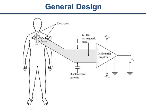
Figure 1. Traditional amplifier.
To enhance performance, a DRL circuit is added to a 3-op-amp paralleling circuit. This is the basis for the improvement of the 3-op-amp circuit. First, an OTA amplifier is added to the original 2-op-amp to enhance the signal amplification effect of this circuit. However adding an amplifier means more power dissipation, so we use fewer resistors to reduce power dissipation and replace the required resistors with appropriate circuit connections. Secondly, the DRL circuit, which is an integral part of the ECG detection circuit, has also undergone some improvements to match the reduced resistance of the 3-op-amp circuit. In the circuit simulation of LT-spice, this project has the frequency of A-B, the gain of C, the noise of D, and the power consumption of E.
2. Properties of ECG signal and requirements of the amplifier
To make the circuit have power consumption and low noise, a CMOS gate input is used, but the circuit’s gain needs to be accurately controlled. The gain of open-loop CMOS amplifiers is difficult to predict. Instead, typically uses op-amps. Biasing of op-amp reduces the input impedance. Also, mismatched components lead to finite CMRR. So, a classic 3-op-amp Instrumentation amp can effectively solve some problems. The advantage of this circuit is that it can increase CMRR. However, it still doesn’t solve the resistor mismatch issue. So using a DRL circuit for the changed circuit to actively ground then setting the host voltage to a value within the common-mode range of the amplifier input.
2.1. The characteristics of the ECG signal
The mV level of the ECG signal is consistent, ranging from 10V to 5mV. The primary energy is concentrated at 0.05 to 100Hz, and the bandwidth ranges from 0-200Hz. There are four different kinds of waves for an ECG signal. The P wave has a bandwidth of 0-8Hz ± 3Hz, while the QRS wave has a bandwidth of 0-55Hz ± 19Hz, and the P wave has a bandwidth of 0-11Hz ± 2Hz. 0-58Hz ± 19Hz is the primary focus of the entire signal bandwidth[9].
2.2. Requirement amplifier
In the field of electronics, the design of portable wearable circuits is very important. Because the power consumption in the traditional circuit design is very huge, it is very detrimental to the endurance of small devices. In the field of circuit design and execution of complicated architectures, there have been new techniques that have emerged. Due to its high power consumption and low CMRR, portable applications are not suitable for the conventionally developed instrumentation amplifier. Therefore, the gain is an important criterion for measuring the quality of an op-amp.
The ECG amplifier in this project must, at minimum, meet the following specifications:
- The frequency range is between 0.1Hz and 250Hz, with a 10% deviation.
- The differential gain is between 40dB and 5 dB.
- The noise level in the input referred to is 4 VRMS.
- The total power consumed by all blocks is 5W.
- The total amount of capacitance employed is 1nF.
3. The construction of a circuit for an ECG amplifier
A 3-op-amp amplifier circuit, a low-pass filter, and a DRL circuit are the foundations for the entire ECG signal amplifier circuit. Two parts make up the circuit: a common-mode extraction circuit and a three-operation amplifier conventional circuit. The circuit utilizes an OTA that is built using the 180nm CMOS model.
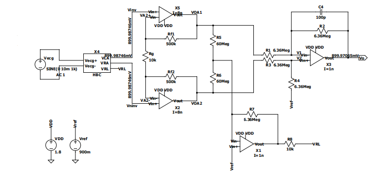
Figure 2. Structure of ECG Amplifier.
The human body resistance analog circuit plays an important role in simulating the effect of human resistance on the circuit. Through continuous testing, finding that the most suitable human resistance value for this circuit. Of course, by changing the resistance of the human body circuit, so obtain the simulation of the ECG signal under different conditions.
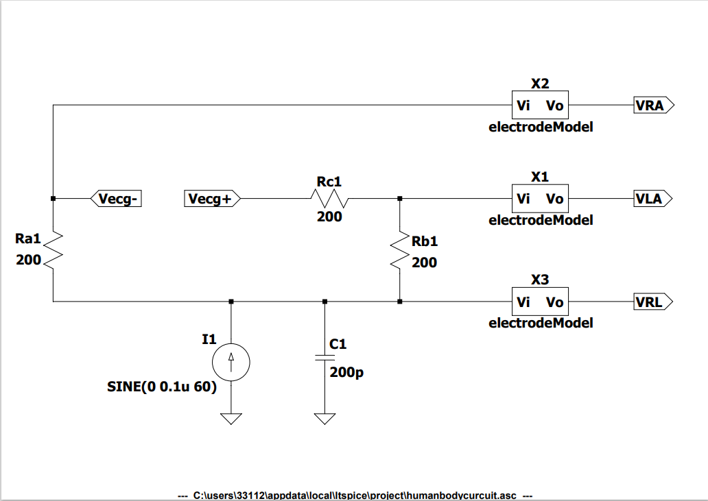
Figure 3. Human body circuit design.
The 3-op-amp circuit and the OTA amplifier design, as shown in Figures 4 and 5 are based on five P-MOSFETs and three N-MOSFETs in one OTA amplifier, which amplifies the collected ECG signal. This part is the most important part of the circuit, which amplifies the signal generated by the human body and transmits it to the later parts. During the design process, first, use an ideal amplifier to experiment with the results. After confirming that the experimental results using the ideal amplifier are correct, the ideal amplifier is replaced with an OTA amplifier to make it an amplifier that can eventually be used in the device. The signal amplification results of this part are finally presented after passing through the DRL circuit and low-pass filter and then analyzed for subsequent analysis.
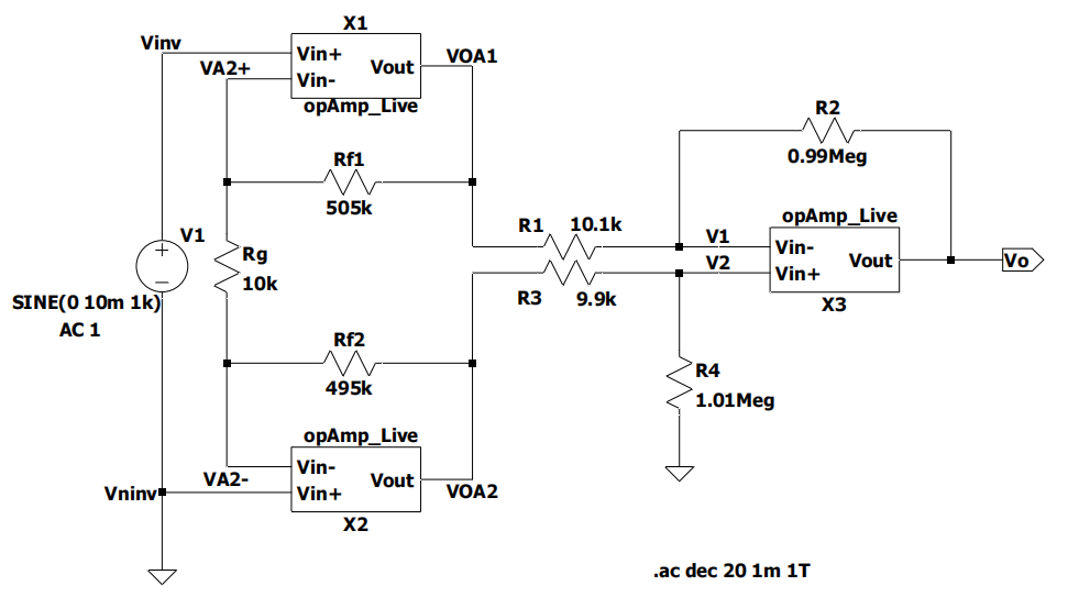
Figure 4. 3-op-amp circuit design.
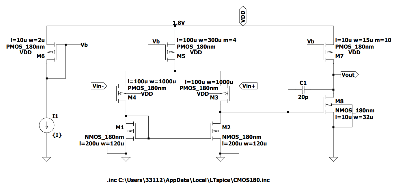
Figure 5. OTA amplifier design.
An op-amp and two resistors are used to build the driven-right leg circuit, as shown in Figure 6. It simulates the signal simulation results obtained by the above amplification circuit after the human body is connected through the right leg to form a loop. It has three main features, physiological small signal detection, suppresses common-mode interference on the electrode transmission line, and improved common-mode rejection ratio CMRR.
Suppose that common-mode interference \( {e_{noise}} \) is parasitically coupled to the two electrode transmission lines.
Then where the two resistors R connect, the signal input to the buffer amplifier should be
\( \frac{1}{2}(2{e_{noise}})={e_{noise}}\ \ \ (1) \)
Finally, the electrode is driven through the right leg, and the signal enters the body \( {e_{noiseecm}} \) should be
\( {e_{noiseecm}}=(1+\frac{{R_{F}}}{{R_{i}}}){V_{ref}}-\frac{{R_{F}}}{{R_{i}}}{e_{noise}}\ \ \ (2) \)
When \( {V_{ref}}=0V \) ,
\( {e_{noiseecm}}=-\frac{{R_{F}}}{{R_{i}}}{e_{noise}}\ \ \ (3) \)
It can be seen that the right leg drive circuit suppresses common-mode interference and improves the CMRR of the system by amplifying the common-mode signal in the reverse phase and entering it into the human body. Let the original common-mode noise be \( {e_{noise0.}} \)
After processing, the common-mode noise input to the instrumentation amplifier is \( {e_{noise}} \) ’ should be satisfied,
\( e_{noise}^{ \prime }={e_{noise0}}-\frac{{R_{F}}}{{R_{i}}}e_{noise}^{ \prime }\ \ \ (4) \)
Solved,
\( e_{noise}^{ \prime }={e_{noise0}}×\frac{1}{1+\frac{{R_{F}}}{{R_{i}}}}\ \ \ (5) \)
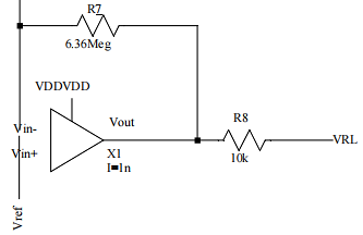
Figure 6. Driven-right leg circuit design.
4. Discussion and simulation
The frequency, CMRR, Differential gain, and noise parameters can be obtained after simulating the entire amplifier circuit with LTspice. The results are shown in the below calculation.
Calculation:
Total integrated input-referred noise:
\( 263.83÷66.83=3.94uV\ \ \ (6) \)
After simulation, the LT-Spice revealed a total power consumption of 4.6733758uW.
Parameter calculation
Stage 1:
\( {A_{v,dm}}=1±\frac{500k+500k}{10k}=40 dB\ \ \ (7) \)
Stage 2:
\( {A_{v, dm}}=-\frac{6.36}{2×6.36}-\frac{6.36(6.36×6.36)}{2×6.36(6.36+6.36)}=0dB\ \ \ (8) \)
LPF:
Frequency and Common Mode Gain:
\( {f_{H}}=\frac{1}{2π×6.36M×100p}=250HZ\ \ \ (9) \)
\( {A_{id}}=36.5dB=66.83\ \ \ (10) \)
\( {A_{cm}}=-76+45=-31dB=0.021\ \ \ (11) \)
\( CMRR=\frac{{A_{id}}}{{A_{cm}}}=3182\ \ \ (12) \)
Noise efficiency factor(NEF):
\( NEF={V_{n,in,RMS}}\sqrt[]{\frac{{I_{tot}}}{{ϕ_{t}}*4KT*BW8*\frac{π}{2}}}=3.945u×\sqrt[]{\frac{2.6uA}{25M×4KT×250×\frac{π}{2}}}=15.8\ \ \ (13) \)
\( K=1.38×{10^{-23}}T=298\ \ \ (14) \)
Table 1. Performance compared with Design requirements.
Frequency range | Differential gain | Total integrated input-referred noise | Total power consumption of all blocks | Total amount of employed capacitance | |
Requirement of this disign | 0.1Hz–250Hz±10% | 40dB±5dB | <4µVRMS | <5µW | <1nF |
This work | 1mHz-258.7Hz | 36.5 | 3.94uV | 4.67uW | 100p |
Table 1 shows the comparison results between my circuit simulation and project requirements. This circuit has met all the requirements of the project.
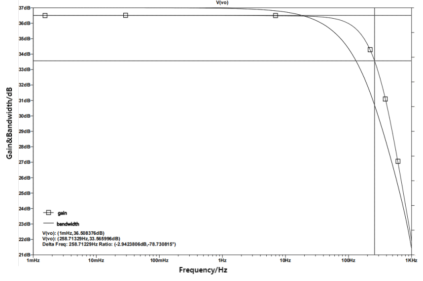
Figure 7. Differential Gain and Bandwidth
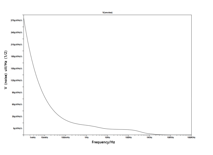
Figure 8. Noise simulation result
Figure 7 shows the gain and bandwidth of the amplifier circuit. Finding out that the transmission band, which during 0.1-250Hz ± 10%. There is no bias in the range and voltage gain of the ECG signal. The requirement mentioned above is met by the highest differential gain reaching 36.508376dB.
The figure of noise simulation is contained in Figure 8. The NEF given in equation (13) is 15.8 and the total integrated input-referred noise is \( 3.94uV \) .
5. Conclusion
In this paper, the shortcomings of traditional ECG signal circuits are first given, and an improvement scheme is given based on them. The result is a standard-compliant low-noise ECG amplifier circuit, on top of which the power consumption is improved. In the preamplifier circuit design, the characteristics of the human ECG signal are referenced. According to the data given, the simulation is carried out, and the final result shows good amplification performance and low noise. Capable of efficient output of ECG signals without significant distortion. In addition, the amplifier devices are powered by a small size power supply, which meets the basic requirements of wearable devices. Based on penetrability, balance its performance, and limit its power consumption and noise parameters. While meeting basic requirements, there is still room for improvement. Finally, some prospects for future design are given.
First of all, In the above experimental results, it can still be seen that it generates a lot of noise, which can have a great impact on ECG signal detection. Therefore, in future circuit design, it is necessary to further reduce the noise and improve the accuracy of the signal. Secondly, because it is a wearable device, its battery life guarantee is not ideal at present, and the power consumption of this circuit still cannot reach the goal of long-term battery life. Power dissipation needs to be reduced by reducing the amplifier impedance on this basis, but its feasibility still needs to be verified by subsequent experiments. This can improve the accuracy of wearable devices to warn people of problems and better protect people from heart disease. Better battery life can also make it possible to detect ECG signals more durably so that people cannot lose the detection of their heart after forgetting to charge once. Finally, the device can access the Internet, and upload the detected signal to the database in real time for comparison, and if there is an abnormal signal, the user will be informed and warned for a certain period. After not getting feedback from the user for some time, an automatic alarm program will be activated to ensure the safety of the user.
References
[1]. Prutchi D and Norris M 2005 Design and Development of Medical Electronic Instrumentation: A Practical Perspective of the Design, Construction, and Test of Medical Devices, (Wiley: Hoboken, NJ, USA) pp. 2–6.
[2]. Thakor N V 1999 Biopotentials and Electro-physiology Measurement (Johns Hopkins School of Medicine: Baltimore, MD, USA).
[3]. Van Helleputte N, Kim S, Kim H, Van Hoof C and Yazicioglu R F 1998 IEEE Trans. Biomed. Circuits Syst. 6 552.
[4]. Ren M Y, Zhang C X, and Sun D S 2012 Procedia Eng. 2 35.
[5]. Yazicloglu R F, Merken P, Puers R, and Van Hoof C 2006, A 60ȣW 60 nV/ҀHz readout front-end for portable biopotential acquisition systems IEEE Int. Solid-State Circuits Conf, pp. 1100-1110.
[6]. Jeon D 2014, An implantable 64nW ECG-monitoring mixed-signal SoC for arrhythmia diagnosis, IEEE Int. Solid-State Circuits Conf., pp. 416-417.
[7]. Suchetha M, Kumaravel N, Jagannath M 2017 Informatics in Medicine Unlocked,8.
[8]. Zhang Chaolong,He Yigang,Yuan Lifeng, 2017 IEEE Access,5 1.
[9]. Chen S C, Hallum L E, Wong Y T, Domme N, Byrnes-Preston P J, Suaning G J, and Lovell N H 2010 Artificial Vision Wiley Encyclopedia of Biomedical Engineering(New York: Wiley–Interscience) pp 1-10.
[10]. Dragomiretskiy K, Zosso D 2014 IEEE Trans. Signal Process., 62 531-544.
Cite this article
Zhao,C. (2024). Low noise, analog electrocardiogram signal amplifier for wearable equipment. Theoretical and Natural Science,30,20-28.
Data availability
The datasets used and/or analyzed during the current study will be available from the authors upon reasonable request.
Disclaimer/Publisher's Note
The statements, opinions and data contained in all publications are solely those of the individual author(s) and contributor(s) and not of EWA Publishing and/or the editor(s). EWA Publishing and/or the editor(s) disclaim responsibility for any injury to people or property resulting from any ideas, methods, instructions or products referred to in the content.
About volume
Volume title: Proceedings of the 3rd International Conference on Computing Innovation and Applied Physics
© 2024 by the author(s). Licensee EWA Publishing, Oxford, UK. This article is an open access article distributed under the terms and
conditions of the Creative Commons Attribution (CC BY) license. Authors who
publish this series agree to the following terms:
1. Authors retain copyright and grant the series right of first publication with the work simultaneously licensed under a Creative Commons
Attribution License that allows others to share the work with an acknowledgment of the work's authorship and initial publication in this
series.
2. Authors are able to enter into separate, additional contractual arrangements for the non-exclusive distribution of the series's published
version of the work (e.g., post it to an institutional repository or publish it in a book), with an acknowledgment of its initial
publication in this series.
3. Authors are permitted and encouraged to post their work online (e.g., in institutional repositories or on their website) prior to and
during the submission process, as it can lead to productive exchanges, as well as earlier and greater citation of published work (See
Open access policy for details).
References
[1]. Prutchi D and Norris M 2005 Design and Development of Medical Electronic Instrumentation: A Practical Perspective of the Design, Construction, and Test of Medical Devices, (Wiley: Hoboken, NJ, USA) pp. 2–6.
[2]. Thakor N V 1999 Biopotentials and Electro-physiology Measurement (Johns Hopkins School of Medicine: Baltimore, MD, USA).
[3]. Van Helleputte N, Kim S, Kim H, Van Hoof C and Yazicioglu R F 1998 IEEE Trans. Biomed. Circuits Syst. 6 552.
[4]. Ren M Y, Zhang C X, and Sun D S 2012 Procedia Eng. 2 35.
[5]. Yazicloglu R F, Merken P, Puers R, and Van Hoof C 2006, A 60ȣW 60 nV/ҀHz readout front-end for portable biopotential acquisition systems IEEE Int. Solid-State Circuits Conf, pp. 1100-1110.
[6]. Jeon D 2014, An implantable 64nW ECG-monitoring mixed-signal SoC for arrhythmia diagnosis, IEEE Int. Solid-State Circuits Conf., pp. 416-417.
[7]. Suchetha M, Kumaravel N, Jagannath M 2017 Informatics in Medicine Unlocked,8.
[8]. Zhang Chaolong,He Yigang,Yuan Lifeng, 2017 IEEE Access,5 1.
[9]. Chen S C, Hallum L E, Wong Y T, Domme N, Byrnes-Preston P J, Suaning G J, and Lovell N H 2010 Artificial Vision Wiley Encyclopedia of Biomedical Engineering(New York: Wiley–Interscience) pp 1-10.
[10]. Dragomiretskiy K, Zosso D 2014 IEEE Trans. Signal Process., 62 531-544.